
 Open Access Article
 This Open Access Article is licensed under a Creative Commons Attribution-Non Commercial 3.0 Unported Licence
Gap separation-controlled nanogap electrodes by molecular ruler electroless gold plating
Victor M.
Serdio V
a,
Taro
Muraki
a,
Shuhei
Takeshita
a,
Daniel E.
Hurtado S
a,
Shinya
Kano
a,
Toshiharu
Teranishi
b and
Yutaka
Majima
*a
aMaterials and Structures Laboratory, Tokyo Institute of Technology, 4259, Nagatsuta-cho, Midori-ku, Yokohama 226-8503, Japan. E-mail: majima@msl.titech.ac.jp
bInstitute for Chemical Research, Kyoto University, Uji 611-0011, Japan
First published on 18th February 2015
Abstract
A simultaneous fabrication process of multiple nanogap electrodes at desired gap separations by the technique of molecular ruler electroless gold plating (MoREP) is reported. Initial gold nanogap electrodes with a gap separation of 22 nm were immersed into MoREP solutions consisting of chloroauric acid, surfactant molecules of alkyltrimethylammonium bromide (CnTAB, n = 12–18) and ascorbic acid as a reducing agent. The electroless plating locally self-terminates between the gap when the surfactant molecules physisorbed to the surface of one electrode interdigitate with the ones of the opposite electrode. The mean nanogap separation correlated with the alkyl chain length, and can be controlled between 2.5 ± 0.6 and 3.3 ± 0.8 nm by choosing the alkyl chain length of the surfactant molecules (C12–C18). A double-gate single-electron transistor (SET) was chemically assembled by introducing chemically a synthesized gold nanoparticle into the MoREP nanogap electrodes, and showed stable Coulomb diamonds under application of both gate voltages.
1. Introduction
As the sizes of nanodevice features decrease to a few nanometers, the integration of functional components into macroscopic electronic circuits presents formidable challenges.1–3 Bottom-up processes have been implemented to connect traditional top-down processes in order to utilize molecules and nanoparticles with specific functions such as negative differential resistance,1,4,5 rectification,1,6–8 memory effects,9–11 and single-electron phenomena.12–15 Nanogap electrodes are promising platform for nanodevices because the single nanometer-sized components can be directly wired between the electrodes in the approach toward solid-state nanodevices.16 Several fabrication techniques for nanogap electrodes have been studied: mechanically controllable break junctions,3,12,17 electromigration,13,15,18 oblique metal evaporation with shadow masks,14,19 electron beam lithography (EBL),20 and electrochemical methods.21,22For practical application, nanogap electrodes must be fabricated simultaneously with high precision.16 Electroless plating is a promising technique for the fabrication of integrated nanogap electrodes.4,23–25 Recently, we established the electroless gold plating (ELGP) technique for the mass production of the robust nanogap electrodes with gap separations of 5 nm or less in 90% yield.25 This ELGP technique is based on a surface-catalyzed chemical deposition of elemental gold. In this process, Ti/Au nanogap electrodes are patterned by EBL with an initial gap separation of ∼22 nm. To grow a gold layer over the electrode surfaces, they are immersed in an ELGP solution made by mixing gold foil, the common antiseptic tincture of iodine and L(+)-ascorbic acid. The growth of the electroless plated layer self-terminates when a gap separation of less than 5 nm is reached, because the mass transport of the gold ions is restricted by the diffusion limit in this narrow space.25 The plating conditions are optimized, and thus robust nanogap electrodes can be simultaneously fabricated with a mean separation (μ) of 3.0 nm and a standard deviation (σ) of 1.7 nm in 90% yield.25
Using the ELGP nanogap electrodes, we fabricated chemically assembled single-electron transistors (SETs) in which a single synthesized gold nanoparticle was chemisorbed between the nanogap electrodes as a Coulomb island using alkanedithiol anchor molecules.26–29 The resulting assemblies exhibited uniform charging energy,26 double side-gated logic operations,27 discrete energy levels for the Au nanoparticles,28 and SiNx passivated SETs.29 However, it is well known that even a variation as small as 0.1 nm in a tunneling barrier can modify the tunneling resistance by one order of magnitude. In terms of single-molecule devices, recent studies have also reported that only a 0.1 nm change in the distance between an electrode and a single molecule strongly affects the electrical transport of the molecule.2,3 As the sizes of functional molecules are unique, much higher controllability of the nanogap separation – on the order of sub-nanometer precision – is required to reproducibly fabricate specific structures for nanodevice applications.
Mixtures of surfactants, ionic gold, and weak reductant (L(+)-ascorbic acid) have been used as ELGP solution for the growth of typically shaped nanostructures. By introducing surfactant molecules, the shape and nanogap separations of the Au nanomaterials can be controlled.30–34 It is reported that an uniform separation between overplated nanocubes is maintained in a few nanometers in length, and that this uniform separation could be attributed to the surfactant molecules.32 However, the chain-length dependence of the separation has not been discussed. We conceived that an ELGP solution with surfactant molecules would be useful for the precise gap separation control of nanogap electrodes.
In this paper, we introduce an ELGP technique which we term molecular ruler electroless plating (MoREP), which more precisely controls the separation of the nanogap electrodes. Four alkyltrimethylammonium bromides–dodecyltrimethylammonium bromide (C12TAB), tetradecyltrimethylammonium bromide (C14TAB), hexadecyltrimethylammonium bromide (C16TAB), and octadecyltrimethylammonium bromide (C18TAB) – constituted the surfactant components of MoREP solution. We correlate the alkyl chain length of the surfactant molecules with the mean nanogap separation. We discuss the self-termination mechanism that occurs during MoREP based on the interdigitation of the surfactant molecules. A double-gate SET was also fabricated to demonstrate the usability of the MoREP nanogap electrodes.
2. Results and discussion
2.1 Electroless plating with surfactant
UV-visible absorption spectroscopy was used to monitor changes in the plating solution; the spectra and a step-wise schematic diagram of the entire chemical reactions are shown in Fig. 1a and b, respectively. In the UV-vis absorption spectrum of the initial HAuCl4 solution, the absorption at 288 nm (blue solid line) disappears after adding the surfactant C12TAB (red solid line). A new peak at 380 nm and a shoulder at 450 nm appear, providing clear evidence of the transformation of the [AuCl4]− ions into [AuBr4]− ions.35,36 Therefore, the first step comprises the ligand substitution of the Cl− ions in [AuCl4]− by Br− ions, as given by reaction (1).| [AuCl4]− + 4Br− → [AuBr4]− + 4Cl− | (1) |
| [AuBr4]− + 2e− → [AuBr2]− + 2Br− | (2) |
| [AuBr2]− + e− → Au0 + 2Br− | (3) |
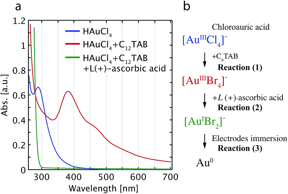 | ||
| Fig. 1 (a) UV-visible spectra of the solution during the three gold complex transformation states. The three curves represent chloroauric acid solution (blue) and after mixing with the surfactant of C12TAB (red), and after the addition of L(+)-ascorbic acid (green). (b) Schematic diagram of the reactions for the formation of [AuBr2]− plating ions and their reduction into Au0 to form the electroless plated layer. | ||
After adding 0.1 M L(+)-ascorbic acid into the plating blend, the solution becomes colorless and transparent (cf.Fig. 1a, green solid line). Mechanistically, the L(+)-ascorbic acid provides two e− upon its dehydration and transforms [AuBr4]− into [AuBr2]−.36 This can be written as reaction (2).
Concomitantly, the third surface-catalyzed chemical reaction proceeds in which the Au+ ions in the gold bromide complexes are reduced to the elemental state (Au0) as in reaction (3). This surface-catalyzed chemical reaction is accelerated due to the negative electrostatic charge on the gold electrodes by the ascorbic acid, which induces the direct reduction of [AuBr2]−.32,33,37 Therefore, when we immerse a sample with clean Au electrodes in the solution, additional gold is electroless plated onto the gold surfaces.
Typical ultra-high resolution scanning electron microscopy (SEM, Hitachi SU8000) images of the nanogap electrodes before and after ELGP with C18TAB are shown in Fig. 2a. From the cross-sectional pixel intensities of the images (Fig. 2b), we accurately determined the nanogap separation at 0.5 nm resolution.
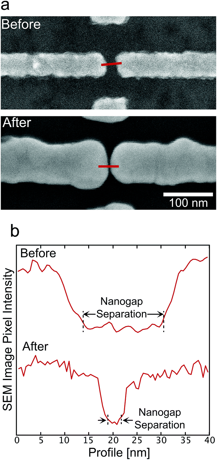 | ||
| Fig. 2 (a) Typical SEM images of the nanogap electrodes before and after the MoREP process with C18TAB. (b) A 50 nm cross section profile of the SEM images in which the pixel intensity is used to accurately determine the nanogap separation. | ||
2.2 Temperature dependence of electroless plating rate
Fig. 3a shows SEM images of the nanogap electrodes after 30 min ELGP processing at different temperatures in the case of C12TAB. At 40 °C, the growth of the plating layer is faster over a larger area. This is because the reduction of [AuBr2]− plating ions is so rapid that Au clusters are generated in the solution. The cluster can physisorb directly on the Au electrodes, which results in corrugated surface or unintentionally interconnected electrodes.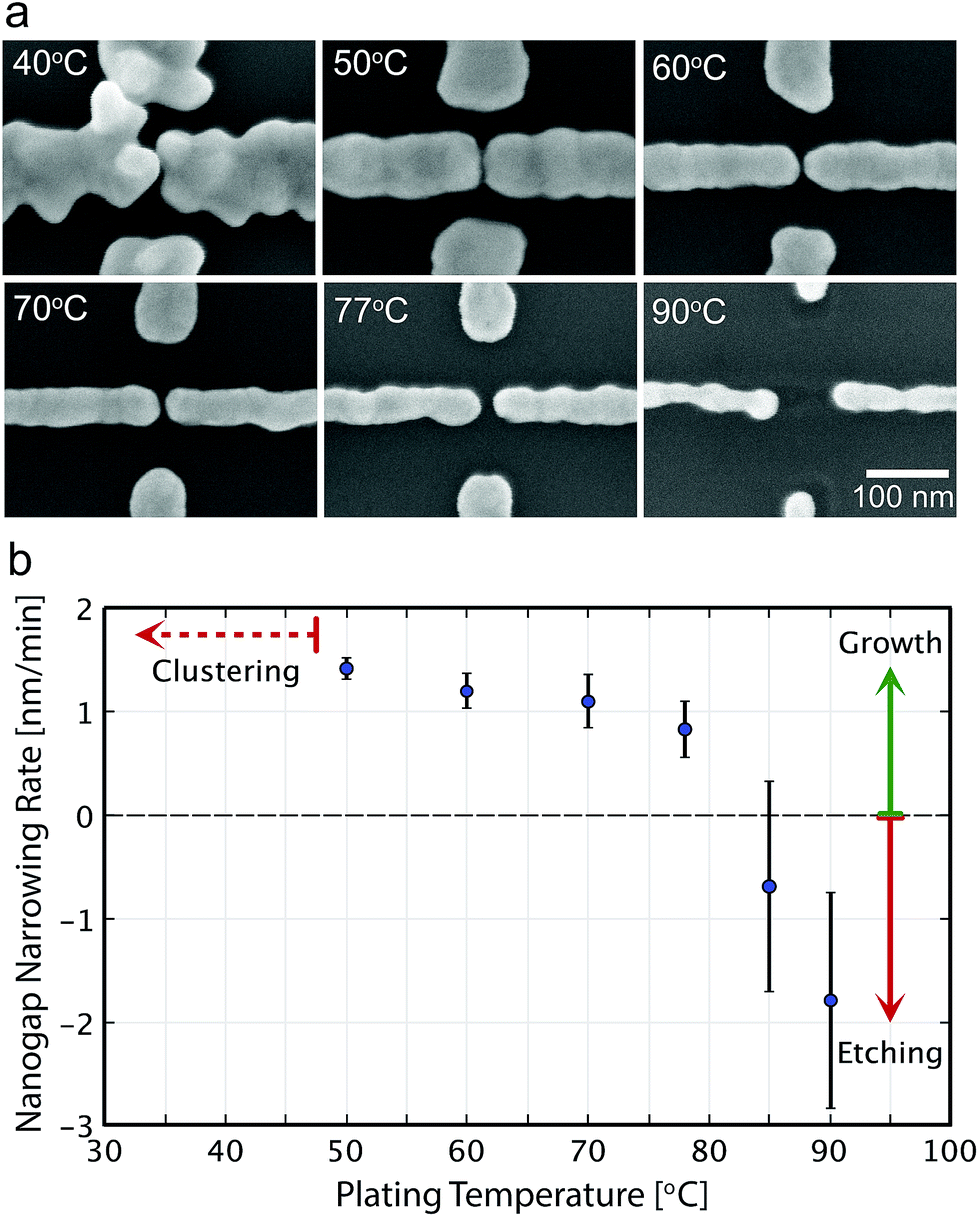 | ||
| Fig. 3 (a) Qualitative and (b) quantitative temperature dependence of the gold layer growth rate in the ELGP process for the case of C12TAB. The averages of the growth rates are calculated for all 30 nanogap electrodes in one ELGP immersion for 30 min (i.e., the same temperature and surfactant molecule). | ||
Between 50 and 77 °C, ELGP process proceed in a good manner as shown in Fig. 3a. The development of surface roughness was suppressed and smooth electrodes surfaces were obtained. The growth rates were calculated for every 30 nanogap electrodes at the temperatures ranging between 50 and 90 °C, and are shown in Fig. 3b. The growth rates decrease as the plating temperature increases. This dependence is attributed to the nonuniform bilayer that is expected to form over the electrodes by the alkyltrimethylammonium bromide component, which can be destabilized by increasing the temperature.38,39
At temperatures over 80 °C, the growth of the electrodes lessens and some etching of the initial electrodes is observed (Fig. 3a and b). At this temperature, the stability of the system is achieved not by the reduction of the plating ions but by the oxidation of [Au0] into [AuBr4]− which is unintentionally promoted and Au atoms on the electrode surfaces dissolve into the solution.40 If L(+)-ascorbic acid becomes insufficient during the ELGP process, especially at the surface of the Au electrodes, the reverse process of plating will occur instead.25 Consequently, the temperature of the electroless plating solution plays an important role, not only in determining the rate of the plating reaction.32,37,41–43
Fig. 4 shows the SEM images of typical nanogap electrodes plated using the C12TAB, C14TAB, C16TAB, and C18TAB surfactants in the electroless plating processes. As shown in Fig. 2a, the initial electrode width was 50 nm. In Fig. 4, the typical electrode widths were between 80 and 100 nm. The electroless plated thickness was estimated as 15–25 nm. On the other hand, the initial gap separation was about 22 nm. As the gap separation narrows both electrodes' sides, the assumed total electroless plated thickness between the gap is clearly larger than the initial gap separation. Consequently, the growth of the electroless plated layer self-terminated during the electroless plating processes.
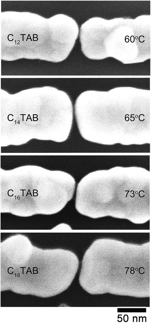 | ||
| Fig. 4 Typical magnified SEM images after ELGP for each of the surfactant molecules of C12TAB, C14TAB, C16TAB, and C18TAB at ELGP solution temperatures of 60, 65, 73, and 78 °C, respectively. | ||
Fig. 5 shows histograms of the nanogap separations for the four surfactants. The mean nanogap separations after ELGP clearly depend on the introduced surfactant and widens with the increasing number of carbon atoms in the surfactant alkyl chain. The plating solution temperature at which to obtain a clear self-terminated nanogap separation was different for each of the surfactants. The temperatures given in the figure indicate the solution temperature employed during the electroless plating processes, which were optimized for each surfactant molecule. The longer surfactant molecules required higher plating temperatures. This variation in the optimal temperature is evidence of the fact that the lengthening of the alkyl chain increases the total attractive interaction between the surfactant tail ends. Therefore, higher thermal energy is required to destabilize the surfactant molecular layer on the gold electrode surface so that the flow of [AuBr2]− plating ions to the gold surface is allowed.
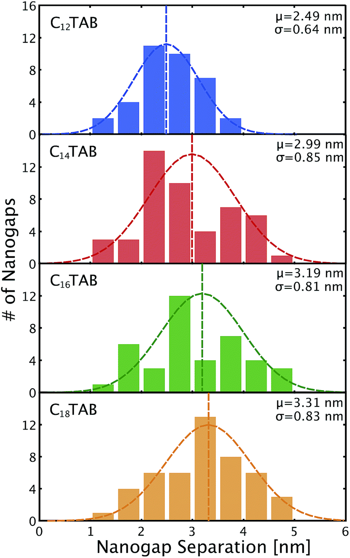 | ||
| Fig. 5 The histograms of nanogap separation for the surfactant molecules of C12TAB, C14TAB, C16TAB, and C18TAB at ELGP solution evaluated by the SEM measuring technique displayed in Fig. 2 with their mean nanogap separations (μ) and standard deviations (σ). | ||
For the self-terminated growth of nanogap electrodes, the criterion of a uniform parallel shape in the separation must be met. As shown in Fig. 4, this criterion was achieved, which proves that electrode growth was limited at the end of the electroless plating process.
2.3 Alkyl chain length dependence of nanogap separation
The dependence of the mean nanogap separation μ on the number of carbon atoms in the alkyl chain of CnTAB is shown in Fig. 6 for C12TAB to C18TAB. The nanogap separations range from 2.5 to 3.3 nm and are correlated to n of the surfactant molecules. The slope of μ per atom is calculated as 0.13 nm per atom. On the contrary, the length of the surfactant molecule CnTAB (Ln) is estimated as Ln = 0.127n + 0.33 nm.44–48 Controllability of the nanogap separation by the surfactant molecules is explained as follows. If bare gold electrodes are immersed in the ELGP solution, the head groups of the surfactant molecules electrostatically physisorb with the gold electrode surface.49,50 This electrostatic bonding property is reversible and allows the electroless plating layer to grow by the reduction of [AuBr2]− ions on the surface when the surfactant molecules are detached. As shown in Fig. 6, the mean nanogap separations after ELGP by using the C12TAB, C14TAB, C16TAB, and C18TAB surfactants were 2.49, 2.99, 3.19 and 3.31 nm, respectively.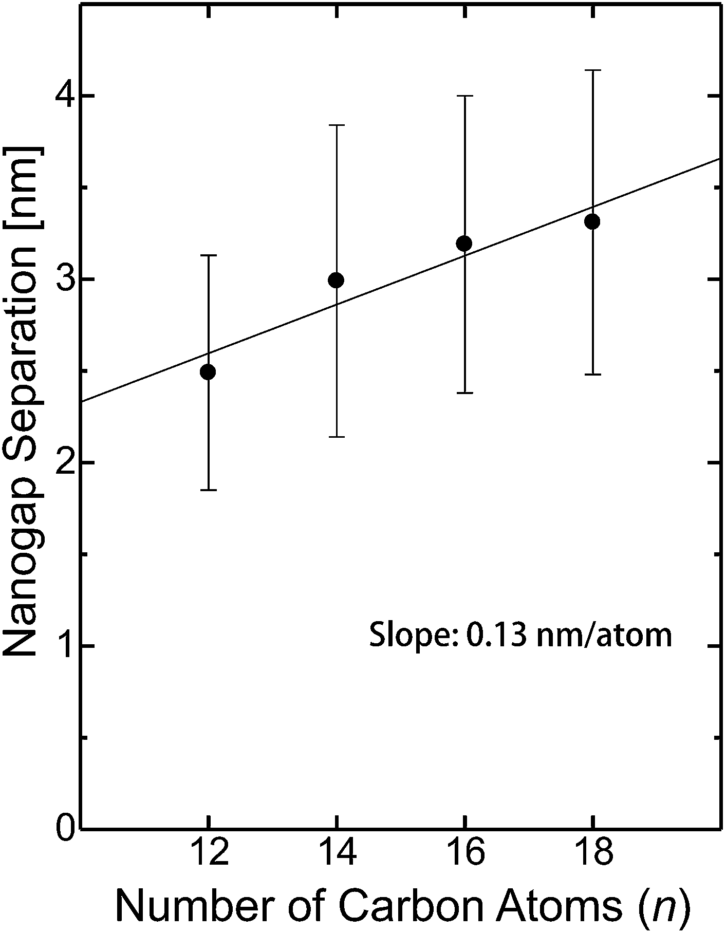 | ||
| Fig. 6 Nanogap separation (μ) dependence on the number of carbon atoms in the alkyl chain of CnTAB. The error bar whiskers represent the standard deviation (σ). | ||
Fig. 7a shows surfactant molecule dependence of the magnified cross-sectional diagrams at their nanogaps. It notes that the surfactant molecules between the nanogap electrodes interdigitate each other, since μ is larger than Ln and is smaller than 2Ln. Assuming perpendicular orientation of CnTAB, the overlap ratios ((2Ln − μ)/Ln), n = 12, 14, 16, and 18 are estimated as 54, 46, 53, and 62%, respectively (Fig. 7b). Due to the bulky tail group of CnTAB, the surfactant molecules should be adsorbed with tilt angle beside substrates.44,48 As a result, the overlap ratios become smaller than the estimated values, however, the alkyl chains of the surfactant molecules should be interdigitated with those from the opposite electrode at the nanogap. Interdigitation suppresses molecular mobilities by van der Waals interactions, thus decreasing the plating growth rate and facilitating self-termination. Consequently, the nanogap separations in the ELGP processes are precisely ruled by the interdigitation of the surfactant molecules as shown in Fig. 7b, therefore this ELGP process should be named as molecular ruler electroless plating (MoREP). Compared to our previous electroless plating technique that used tincture of iodine and resulted in μ = 3.0 ± 1.7 nm,25 both μ and its standard deviation σ are clearly decreased in the case of C12TAB (μ = 2.5 ± 0.64 nm).
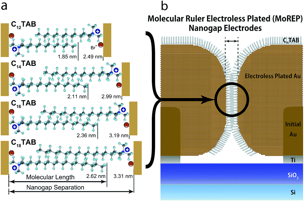 | ||
| Fig. 7 (a) Surfactant molecules dependence of the magnified cross-sectional diagrams at their nanogaps. Experimental mean values of the nanogap separations and their corresponding molecular lengths are displayed based on the interdigitation of the tail section for each of the alkyltrimethylammonium bromide molecules. It notes that the CnTAB should be adsorbed with tilt angle beside substrates due to the bulky tail group of CnTAB. (b) Cross-sectional diagram of the MoREP nanogap electrodes after ELGP. Surfactant molecules interact with the gold surface of the electrodes. The growth of the electroless-plating layer in the nanogap section is self-terminated by the interdigitation of the surfactant molecules. | ||
As shown in Fig. 7b, the surface of the MoREP nanogap electrodes is covered by the surfactant molecules. As the electrostatic physisorption of the surfactant molecules is apparently weaker than the covalent bond between gold and sulfur,51,52 the surfactant molecules can be replaced with alkanethiols only by immersing the sample into their solutions.
To better understand the structure of the nanogap electrodes and the uniformity of the MoREP process, parallel nanogap electrodes were developed as shown in Fig. 8. After the MoREP process, uniform gap separation and smooth surface can be clearly observed (Fig. 8c). The tilt view enables us to see that uniform separation can be obtained from the bottom to the top of the electrodes (Fig. 8d). These three nanogap electrodes are not short-circuited. This uniform parallel separation is a critical advantage for nanodevice applications such as single-electron transistors and molecular devices. Insulation breakdown between the electrodes is a possibility and will be allocated where the interface bottle-necks by the closest approach; thus, the randomness of the separation limits the applicable voltage between the nanogap electrodes. Voltages higher than 1 V are required to utilize the intriguing properties of functional organic molecules.5,9,10 This means that nanogap electrodes must withstand huge electric fields on the order of 4 MV cm−1 in the case of a 2.5 nm gap. Therefore, the uniformity of the nanogap separation can affect the decisive breakdown voltage of the devices and their stable operation.
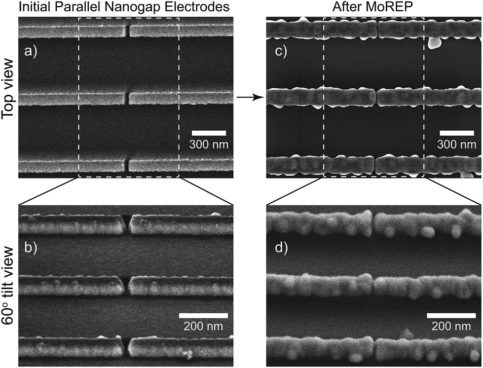 | ||
| Fig. 8 SEM images of the initial parallel nanogap electrodes after EBL lithography with a (a) top view and (b) 60° tilt angle, as well as the parallel nanogap electrodes after the MoREP process with a (c) top view and (d) 60° tilt angle. | ||
2.4 Application of MoREP nanogap electrodes for SETs
To prove the compatibility of the nanogap electrodes made by MoREP in nanodevice applications, we fabricated a double side-gated SET using the MoREP nanogap electrodes. Inset of Fig. 9a shows the SEM image of the double side-gated SET consists of the MoREP nanogap electrodes and a single gold nanoparticle (NP). After the preparation of the MoREP nanogap electrodes with C18TAB, the chemical assembly processes for SETs were employed the same as previous our reports.26–28 Between the MoREP nanogap electrodes, the single NP clearly be observed, that behaves as Coulomb island. Fig. 9a shows the Id–Vd characteristics at two gate voltages, Vg1 = 10 V and −1.0 V, where the fractional residual charges on the nanoparticle Q0 have values of e/2 (on state) and 0 (off state), respectively. Clear Coulomb staircases were observed, which can be fully explained by the conventional orthodox theory for a single-dot SET system.53,54 The equivalent circuit of the double-gated SET is shown in Fig. 9a (inset). The SET circuit parameters are the capacitance between the Au nanoparticle core and the source electrode (C1) or the drain electrode (C2), the tunneling resistance between the Au nanoparticle core and the source electrode (R1) or the drain electrode (R2), and the gate capacitance to the two side-gate electrodes (Cg1 and Cg2). The theoretical curves obtained by the orthodox theory are in good agreement with the experimental result, using the parameters C1 = 1.65 aF, C2 = 1.40 aF, R1 = 24 MΩ, and R2 = 320 MΩ. Fig. 9b and c show the experimental differential conductance dId/dVd plots in the gate 1 voltage Vd–Vg1 and the gate 2 voltage Vd–Vg2 planes, respectively. Identical stable Coulomb diamonds can be observed in both side-gate electrodes. The stable characteristics are a result of the chemically assembled Au nanoparticle anchored by decanedithiol (C10S2) in the mixed self-assembled monolayers (SAMs) of octanethiol (C8S) and C10S2. The gate capacitances Cg1 and Cg2 are evaluated as 7.5 and 8.6 zF from the width of the Coulomb diamond along the Vg axis. These values imply symmetrical structures from the gold nanoparticle to the two side-gates. We attribute this symmetrical structure to the uniformity of the nanogap electrodes prepared by the MoREP process. This symmetrical structure is important for realizing logic gates using double-gated SETs because every switching voltage to the side-gate inputs can be identical.27 We believe the MoREP process enables the symmetrical interconnection of a nanoparticle to harness its electrical properties for integration as double-gated SETs.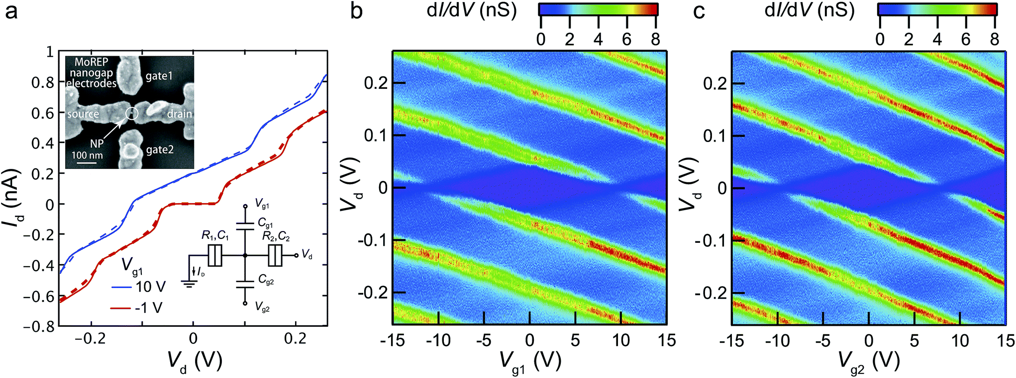 | ||
| Fig. 9 SEM image of double side-gated single-electron transistor consists of the MoREP nanogap electrodes and a single gold nanoparticle (NP) (inset of (a)). (a) Id–Vd characteristics at Vg1 = 10 V (on state, blue curves) and −1 V (off state, red curves) at 9 K. Solid and dashed curves represent the experimental results and the theoretical curves calculated by orthodox theory, respectively (C1 = 1.65 aF, C2 = 1.40 aF, R1 = 24 MΩ, and R2 = 320 MΩ). Inset: equivalent circuit of the double side gates SET. Experimental stability diagrams (dId/dVd) plot in the (b) Vg1–Vd and (c) Vg2–Vd planes at 9 K. | ||
The previously reported ELGP technique based on iodine tincture allow us to develop the necessary templates for the assembly of SETs at the mean gap separation of 3.0 nm,25 stable at room temperature, and atmospheric pressure, and towards O2 plasma treatments. We confirmed that the structure of the nanogap electrodes developed by MoREP present all these characteristics with the great advantage of controllability at the smaller gap separation (μ = 2.5 nm) with smaller standard deviation of 0.64 nm (in the case of C12TAB) which approaches the requirements of sub-nanometer precision in fabricating reproducible single-molecular devices.2,3 Consequently, nanogap electrodes made by MoREP are promising not only for the simultaneous fabrication of nanodevices but for identical transports based on the electronic and structural properties of nanomaterials.
3. Experimental
3.1 Nanogap electrodes fabrication and plating process
Fabrication began with the development of the initial nanogap electrodes. A pattern was drawn by EBL (Elionix, ELS-7500EX) with a gap separation of ∼22 nm. The electrodes consist of a 2 nm Ti adhesion layer on a Si/SiO2 substrate, patterned by EBL and overlaid by a 10 nm layer of Au by evaporation. After the electron-beam resist lift-off process, the Au surface was cleaned by sequential treatment with boiling acetone, boiling ethanol, and ultrasonic deionized water baths. Finally, the complete removal of any contaminants on the gold electrodes was achieved by isotropic oxygen plasma treatment for 5 min and UV-ozone cleaning for 10 min.The plating solution was prepared by first combining an alkyltrimethylammonium bromide surfactant (to interact with the electrode surface) with chloroauric acid (HAuCl4·4H2O, 99.9%, Wako Pure Chemical Industries Ltd.), followed by addition of the L(+)-ascorbic acid reducing agent. The four surfactants [dodecyltrimethylammonium bromide (C12TAB), tetradecyltrimethylammonium bromide (C14TAB), hexadecyltrimethylammonium bromide (C16TAB), and octadecyltrimethylammonium bromide (C18TAB)] were purchased from Tokyo Chemical Industry Co. Ltd. A sample preparation follows: chloroauric acid (50 mM, 120 μl) and aqueous alkyltrimethylammonium bromide (25 mM, 28 ml) were mixed with magnetic stirring, affording a color change in the solution from transparent yellow to opaque orange. Then, aqueous L(+)-ascorbic acid (0.1 M, 3.6 ml, 99.6%) was added and the solution became colorless and transparent. A small amount of acetic acid (1, 1.5, 2 and 2 ml for C12TAB, C14TAB, C16TAB, and C18TAB surfactants, respectively, WAKO) was added in the solution to depress the growth rate.40 All of the solutions used in these processes were prepared with distilled and de-ionized water (18 MΩ).
The initially prepared electrodes with 22 nm gaps were immersed into the plating solution which is in a beaker over a hot plate with magnetic stirring. The hot plate allowed us to control the plating temperature for each particular surfactant molecule, with a range of 60 to 80 °C and stirring helped provide a constant supply of plating ions at the gold surface. After 30 min immersion, growth of the plating layer over the electrodes was self-terminated as a result of the interdigitation of the surfactant molecules.
3.2 SET fabrication and electrical characterization
MoREP nanogap electrodes were chemically assembled into double side-gated SETs as previous reports.26–28 The SEM images of the MoREP nanogap electrodes were observed before the introduction of Au NPs. As amorphous carbon was deposited onto the surface of the nanogap electrode during the observation of SEM images, the amorphous carbon was removed by O2 plasma treatment. The substrate was immersed in C8S (1 mM in ethanol) for 24 h, and then in C10S2 (500 mM in ethanol). Finally, the substrate was immersed in a toluene solution of the decanethiol protected Au NPs, whose core diameters of 6.2 ± 0.8 nm, as estimated by transmission electron microscopy.26–28The electrical characteristics of the devices were measured at 9 K using a mechanical refrigerator-type probe (GRAIL10-LOGOS01S, Nagase Techno-Engineering Co., Ltd., Japan) and a semiconductor device analyzer (B1500, Agilent, USA). The value of dId/dVd was derived by numerically differentiating the Id–Vd curve directly. The theoretical curves are calculated by orthodox theory.53–55
4. Conclusions
The molecular ruler electroless plating (MoREP) process for the fabrication of precise gold nanogap electrodes at desired gap separation was demonstrated. A gold layer grows over the electrode surface during MoREP, and the narrowing gap separation was self-terminated based on the interdigitation of the surfactant molecules between the electrodes. As the gap separation was correlated to the length of the alkyl chain, it can be controlled between 2.5 ± 0.6 and 3.3 ± 0.8 nm by choosing the alkyl chain length of the surfactant molecules (CnTAB, n = 12–18). The mean nanogap separation of 2.5 nm is also smaller than that of our previous paper (3.0 ± 1.7 nm). A chemically-assembled double-gate single-electron transistor was fabricated to demonstrate the usability of the MoREP nanogap electrodes, which exhibit ideal, stable, and reproducible Coulomb diamonds. MoREP, with the ability to control nanogap separations with standard deviations of less than one nanometer, allows us to prepare made-to-order nanogap electrodes by adjusting gap separations to the sizes of the nanoparticles and functional molecules, for the fabrication of ideal single nanoscale solid state devices.Acknowledgements
The authors thank Ms Michiyo Miyakawa for technical support regarding SEM characterization. This study was partially supported by the Elements Strategy Initiative to Form a Core Research Center, funded by the Ministry of Education, Culture, Sports, Science and Technology (MEXT); by the Collaborative Research Project of the Materials and Structures Laboratory, Tokyo Institute of Technology; by the Collaborative Research Program of Institute for Chemical Research, Kyoto University (no. 2014-73); and by the BK Plus program, Basic Science Research program (NRF-2014R1A1030419).References
- J. Chen, T. Lee, J. Su, W. Wang and M. A. Reed, Molecular Electronic Devices, in Molecular Nanoelectronics, ed. M. A. Reed and T. Lee, American Scientific Publishers, 2003, pp. 1–76 Search PubMed.
- K. Moth-Poulsen and T. Bjornholm, Nat. Nanotechnol., 2009, 4, 551 CrossRef CAS PubMed.
- M. L. Perrin, C. J. O. Verzijl, C. A. Martin, A. J. Shaikh, R. Eelkema, H. van EschJan, J. M. van Ruitenbeek, J. M. Thijssen, H. S. J. van der Zant and D. Dulic, Nat. Nanotechnol., 2013, 8, 282 CrossRef CAS PubMed.
- Y. Yasutake, K. Kono, M. Kanehara, T. Teranishi, M. R. Buitelaar, C. G. Smith and Y. Majima, Appl. Phys. Lett., 2007, 91, 203107 CrossRef PubMed.
- Y. Majima, D. Ogawa, M. Iwamoto, Y. Azuma, E. Tsurumaki and A. Osuka, J. Am. Chem. Soc., 2013, 135, 14159–14166 CrossRef CAS PubMed.
- W. Lu and C. M. Lieber, Nat. Mater., 2007, 6, 841–850 CrossRef CAS PubMed.
- A. Aviram and M. A. Ratner, Chem. Phys. Lett., 1974, 29, 277–283 CrossRef CAS.
- C. Joachim, J. K. Gimzewski and A. Aviram, Nature, 2000, 408, 541–548 CrossRef CAS PubMed.
- S. W. Wu, N. Ogawa, G. V. Nazin and W. Ho, J. Phys. Chem. C, 2008, 112, 5241–5244 CAS.
- S. Kano, Y. Yamada, K. Tanaka and Y. Majima, Appl. Phys. Lett., 2012, 100, 053101 CrossRef PubMed.
- H. Koo, S. Kano, D. Tanaka, M. Sakamoto, T. Teranishi, G. Cho and Y. Majima, Appl. Phys. Lett., 2012, 101, 083115 CrossRef PubMed.
- M. A. Reed, C. Zhou, C. J. Muller, T. P. Burgin and J. M. Tour, Science, 1997, 278, 252–254 CrossRef CAS.
- H. Park, J. Park, A. K. L. Lim, E. H. Anderson, A. P. Alivisatos and P. L. McEuen, Nature, 2000, 407, 57–60 CrossRef PubMed.
- S. Kubatkin, A. Danilov, M. Hjort, J. Cornil, J.-L. Bredas, N. Stuhr-Hansen, P. Hedegard and T. Bjornholm, Nature, 2003, 425, 698–701 CrossRef CAS PubMed.
- A. N. Pasupathy, R. C. Bialczak, J. Martinek, J. E. Grose, L. A. K. Donev, P. L. McEuen and D. C. Ralph, Science, 2004, 306, 86–89 CrossRef CAS PubMed.
- T. Li, W. Hu and D. Zhu, Adv. Mater., 2010, 22, 286–300 CrossRef CAS PubMed.
- M.-H. Jo, J. E. Grose, K. Baheti, M. M. Deshmukh, J. J. Sokol, E. M. Rumberger, D. N. Hendrickson, J. R. Long, H. Park and D. C. Ralph, Nano Lett., 2006, 6, 2014–2020 CrossRef CAS PubMed.
- T. Taychatanapat, K. I. Bolotin, F. Kuemmeth and D. C. Ralph, Nano Lett., 2007, 7, 652–656 CrossRef CAS PubMed.
- G. C. Gazzadi, E. Angeli, P. Facci and S. Frabboni, Appl. Phys. Lett., 2006, 89, 173112 CrossRef PubMed.
- M. S. M. Saifullah, T. Ondaruhu, D. K. Koltsov, C. Joachim and M. E. Welland, Nanotechnology, 2002, 13, 659 CrossRef CAS; M. Manheller, S. Trellenkamp, R. Waser and S. Karthauser, Nanotechnology, 2012, 23, 125302 CrossRef PubMed.
- A. F. Morpurgo, C. M. Marcus and D. B. Robinson, Appl. Phys. Lett., 1999, 74, 2084–2086 CrossRef CAS PubMed.
- Y. Kashimura, H. Nakashima, K. Furukawa and K. Torimitsu, Thin Solid Films, 2003, 438–439, 317–321 CrossRef CAS.
- C. S. Ah, Y. J. Yun, J. S. Lee, H. J. Park, D. H. Ha and W. S. Yun, Appl. Phys. Lett., 2006, 88, 133116 CrossRef PubMed.
- G. G. Jang, P. Blake and K. Roper, Langmuir, 2013, 29, 5476–5486 CrossRef CAS PubMed.
- V. M. Serdio V, Y. Azuma, S. Takeshita, T. Muraki, T. Teranishi and Y. Majima, Nanoscale, 2012, 4, 7161–7167 RSC.
- N. Okabayashi, K. Maeda, T. Muraki, D. Tanaka, M. Sakamoto, T. Teranishi and Y. Majima, Appl. Phys. Lett., 2012, 100, 033101 CrossRef PubMed.
- K. Maeda, N. Okabayashi, S. Kano, S. Takeshita, D. Tanaka, M. Sakamoto, T. Teranishi and Y. Majima, ACS Nano, 2012, 6, 2798–2803 CrossRef CAS PubMed.
- S. Kano, Y. Azuma, K. Maeda, D. Tanaka, M. Sakamoto, T. Teranishi, L. W. Smith, C. G. Smith and Y. Majima, ACS Nano, 2012, 6, 9972–9977 CrossRef CAS PubMed.
- G. Hackenberger, Y. Azuma, S. Kano, D. Tanaka, M. Sakamoto, T. Teranishi, Y. Ohno, K. Maehashi, K. Matsumoto and Y. Majima, Jpn. J. Appl. Phys., 2013, 52, 110101 CrossRef.
- T. Teranishi, S. Hasegawa, T. Shimizu and M. Miyake, Adv. Mater., 2001, 13, 1699–1701 CrossRef CAS.
- T. K. Sau and C. J. Murphy, J. Am. Chem. Soc., 2004, 126, 8648–8649 CrossRef CAS PubMed.
- E. Dovgolevsky and H. Haick, Small, 2008, 4, 2059–2066 CrossRef CAS PubMed.
- J. A. Edgar, A. M. McDonagh and M. B. Cortie, ACS Nano, 2012, 6, 1116–1125 CrossRef CAS PubMed.
- T. H. Ha, H.-J. Koo and B. H. Chung, J. Phys. Chem. C, 2007, 111, 1123–1130 CAS.
- O. R. Miranda, N. R. Dollahon and T. S. Ahmadi, Cryst. Growth Des., 2006, 6, 2747–2753 CAS.
- D. H. Evans and J. J. Lingane, J. Electroanal. Chem., 1963, 6, 1–10 CAS.
- K. Sun, J. Qiu, J. Liu and Y. Miao, J. Mater. Sci., 2009, 44, 754–758 CrossRef CAS PubMed.
- L. Gou and C. J. Murphy, Chem. Mater., 2005, 17, 3668–3672 CrossRef CAS.
- B. Nikoobakht and M. A. El-Sayed, Langmuir, 2001, 17, 6368–6374 CrossRef CAS.
- C.-K. Tsung, X. Kou, Q. Shi, J. Zhang, M. H. Yeung, J. Wang and G. D. Stucky, J. Am. Chem. Soc., 2006, 128, 5352–5353 CrossRef CAS PubMed.
- B. Nikoobakht and M. A. El-Sayed, Chem. Mater., 2003, 15, 1957–1962 CrossRef CAS.
- K.-T. Yong, Y. Sahoo, M. Swihart, P. Schneeberger and P. Prasad, Top. Catal., 2008, 47, 49–60 CrossRef CAS.
- M. Muzikar, V. Komanicky and W. Fawcett, J. Cryst. Growth, 2006, 290, 615–620 CrossRef CAS PubMed.
- L. A. Bumm, J. Arnold, D. Dunbar, D. L. Allara and P. S. Weiss, J. Phys. Chem. B, 1999, 103, 8122 CrossRef CAS.
- D. J. Wold and C. D. Frisbie, J. Am. Chem. Soc., 2000, 122, 2970 CrossRef CAS.
- J. M. Mellott and D. K. Schwartz, J. Am. Chem. Soc., 2004, 126, 9369–9373 CrossRef CAS PubMed.
- J. M. Mellott, W. A. Hayes and D. K. Schwartz, Langmuir, 2004, 20, 2341–2348 CrossRef CAS.
- J.-F. Liu and W. A. Ducker, J. Phys. Chem. B, 1999, 103, 8558–8567 CrossRef CAS.
- M. Jaschke, H.-J. Butt, H. E. Gaub and S. Manne, Langmuir, 1997, 13, 1381–1384 CrossRef CAS.
- J. P. Vivek and I. J. Burgess, Langmuir, 2012, 28, 5031–5039 CrossRef CAS PubMed.
- H. Häkkinen, Nat. Chem., 2012, 4, 443 CrossRef PubMed.
- F. Chen, X. Li, J. Hihath, Z. Huang and N. Tao, J. Am. Chem. Soc., 2006, 128, 15874 CrossRef CAS PubMed.
- H. Zhang, Y. Yasutake, Y. Shichibu, T. Teranishi and Y. Majima, Phys. Rev. B: Condens. Matter Mater. Phys., 2005, 72, 205441 CrossRef.
- A. E. Hanna and M. Tinkham, Phys. Rev. B: Condens. Matter Mater. Phys., 1991, 44, 5919–5922 CrossRef.
- S. Kano, T. Tada and Y. Majima, Chem. Soc. Rev., 2015, 44, 970 RSC.
| This journal is © The Royal Society of Chemistry 2015 |