
 Open Access Article
 This Open Access Article is licensed under a Creative Commons Attribution-Non Commercial 3.0 Unported Licence
Highly sensitive on-chip fluorescence sensor with integrated fully solution processed organic light sources and detectors
Z.
Shu†
 *ab,
F.
Kemper†
ab,
E.
Beckert
*a,
R.
Eberhardt
a and
A.
Tünnermann
ab
*ab,
F.
Kemper†
ab,
E.
Beckert
*a,
R.
Eberhardt
a and
A.
Tünnermann
ab
aFraunhofer Institute for Applied Optics and Precision Engineering (IOF), Albert-Einstein-Str. 7, D-07745 Jena, Germany. E-mail: Erik.Beckert@iof.fraunhofer.de
bInstitute of Applied Physics, Abbe Center of Photonics (ACP), Friedrich Schiller University Jena, Max-Wien-Platz 1, D-07743 Jena, Germany
First published on 17th May 2017
Abstract
We report the first fluorescence light detector combining a fully solution processed organic electrochemical cell (OLEC) and a fully solution processed organic photodiode (OPD) within one microfluidic chip. The blue OLEC was used as the excitation source, whereas the OPD was used for detection of the emitted fluorescent light. Two orthogonally oriented linear polarizers were used as excitation and emission filters, enabling the use of fluorescent dyes with emission and absorption peaks very close to each other. In addition the system is compatible with many different fluorescent dyes. The filters and organic devices were mounted onto a microfluidic glass chip. Fluorescein amidite (FAM) was used as a model dye to characterize and demonstrate the concept of the system. Despite a very close excitation peak (492 nm) and emission peak (518 nm) of FAM, we were able to detect FAM concentrations as low as 1 μM even for a brightness value of the OLEC as low as 500 cd m−2. This opens the possibility of producing low cost, portable and disposable fluorescence sensors with a high sensitivity.
Introduction
Microfluidic Lab-on-a-Chip (LoC) systems are widely used in chemistry, biology and medicine since they can provide full sample analysis without the need for bulky and expensive laboratory equipment.1,2 They provide short measurement times by requiring very low amounts of analyte. By the use of cost-efficient replicated polymer chips and solution processing for the integrated functionalities, LoC systems are disposable and suitable for point-of-care applications.3 Within the last few years much effort has been devoted to increasing the degree of integration at reasonable cost and therefore the number and complexity of possible application cases via integrating multi-functionalities and bio-sensors onto microfluidic chips.4–6 Some examples are: on-chip integrated micro-pumps were integrated by fully inkjet-printed piezoelectric membrane pumps7,8 to drive the fluid with analytes through micro-channels; inkjet printed micro-heaters9–11 were integrated to realize the thermal control for analysis; inkjet printed SERS pads were integrated to increase Raman signals;12 the analyte mixing and separating can be digitally controlled by inkjet-printed digital microfluidics;13,14 even micro-channels can be directly printed on paper.15,16Fluorescent sensing is the most common analytical and diagnostic method in biological and medical applications because of high sensitivity and selectivity.17 However, very few examples of fully integrated, compact and low cost fluorescence sensing systems on microfluidic chips can be found. This is mostly because of widely used sensing units based on LASERs, LEDs, CCDs and silicon photodiodes have relatively large dimensions, are relatively expensive and can only be integrated by means of assembly.18 In contrast, organic electronics provide the advantages of direct on-chip integration, easy emission and detection wavelength tuning, compatibility with flexible substrates.19 Furthermore, instead of deposited via vacuum process, organic material can be dissolved into solvents and processed from solution,20i.e. solution processing deposition method, which can highly reduce manufactory cost. This includes but not limited to spin-coating, spray coating, dip coating, slot-die coating and printing methods such as inkjet, screen, gravure printing. Consequently, several integrated organic light-emitting diodes (OLEDs) as well as organic photodiodes (OPDs) fluorescent sensing systems have been reported in recent years.21–26 However, all the OLEDs and OPDs are either fully or partly manufactured by thermal evaporation in a high vacuum, which highly increases the cost, highly reduces the design flexibility because of shadow or lithography masks, and limits integration on flexible and polymeric substrates. The vacuum evaporation method is necessary because of the required low work-function metal layers (e.g. Ba, Ca, LiF) for efficient electron injection. Even though there is tremendous efforts in developing inkjet printed or fully solution processed OLEDs, devices were only partly inkjet printed.27,28 Moreover, ITO anode and/or evaporated metal cathode(s) were still used.29 In this paper, we introduce organic light-emitting electrochemical cells (OLEC)30 as fully solution processable excitation light sources as an alternative to OLEDs for on-chip microfluidic fluorescent sensors. OLECs, in principle, share the same working mechanism as OLEDs. In addition, ionic dopants, which consist of metal salts as ionic donors and an electrolyte to improve ionic mobility, are added into the light-emitting active layer in order to in situ generate a PN-junction within the active layer via electrochemical doping and ion re-distribution. Thanks to the in situ generated PN-junction, air-stable and solution processable electrodes such as silver and PEDOT:PSS can be used. Moreover, OLECs achieve good device performance with much thicker active layers and on rough surfaces,31 which is the one of the current challenges in solution processing and, in particular, OLED printing. As reported previously, sufficient brightness for fluorescent excitation can be achieved for disposable on-chip fluorescent sensing.32 It was also demonstrated that higher emitted brightness can be realized via a tandem device architecture, while high design flexibility can be realized via combination of inkjet printing and spin-coating.33 Another big advantage of OLECs is the consistency of device architecture and fabrication process: no modification is required for different emission wavelengths, i.e. colors, of different fluorescent dyes except the changing of the light-emitting polymers or small molecules. Even for OLEDs, different hole/electron injection and transporting layers should be modified to adapt to different light-emitting materials due to work-function mismatch, especially for blue emitting emitters. This increases the allowed complexity in integrating multiple excitation light sources (OLEDs) for multi-sensing analytes with various fluorescent dyes.
Besides the light source, a sensitive photodetector is necessary to perform fluorescent light detection. OPDs are a cost efficient alternative to conventional silicon based detectors. They can provide a very simple layer stack combining p-semiconductors and n-semiconductors in the bulk hetero junction approach.34,35 To make them fully solution processable an inverted layer stack was introduced36 having a transparent cathode layer instead of a transparent anode. Besides simplifying the manufacture of the OPDs it is also beneficial for the device lifetime. Furthermore, similar to OLECs, by replacing the active polymer, other absorption spectra can be addressed such as deep red and NIR.37–39 To shield the detector from excitation light, filters must be included into the microfluidic chip. In the past different light filter concepts for integration into LoC systems have been studied such as polarization filters,22 colorant filters,40,41 interference filters41 and liquid crystal filters.42 All these filter concepts have different advantages and disadvantages. Colorant filters for example have a high transmission (>95%) in their transmission band compared to polarization filters (<50%). Their drawback is their potential use in only one special application. In order to produce an universally usable microfluidic fluorescent measurement system we selected polarization filters for our work. These filters transmit light in a wide spectral range and are therefore suitable for a large variety of different fluorescent dyes.
In this paper, we introduce the first integrated fluorescent sensing system based on a fully solution processed OLEC and fully solution processed OPD on a glass chip. Selecting polarization filters makes the LoC utilizable for a variety of applications. Blue excitation light and fluorescein amidite (FAM) fluorescent dye were selected for demonstration as they are widely used in fluorescent bio-/chemical sensing. The demonstrated integrated fluorescent sensor is able to measure a low concentration of fluorescent dye, i.e. FAM in water in this case, as low as 1 μM. This is better than the literature reported comparable sensing system with an evaporated OLED and OPD combination.22,26 Furthermore, thanks to the fully solution processing and vacuum free fabrication and easy tuning of the excitation light color, fluorescent sensors based on OLEC, OPD, and linear polarization filters enable a bright future for low-cost, disposable, multi-usage point-of-care applications.
Experimental
Materials
Pre-patterned indium-tin-oxide (ITO) glass substrates, poly(3-hexylthiophene-2,5-diyl) (P3HT), and phenyl-C61-butyric acid methyl ester (PCBM) were purchased from Ossila Ltd. Blue light-emitting polymer (SPB-02T) was purchased from Merck KGaA. Zinc acetylacetonate hydrate (Zn(acac)2) precursor, solid electrolyte dicyclohexano-18-crown-6 (DCH18C6), and dopant salt lithium trifluoromethanesulfonate (LiCF3SO3) were purchased from Sigma-Aldrich Chemie GmbH. Highly conductive poly(3,4-ethylenedioxythiophene) – poly(styrenesulfonate) (PEDOT:PSS CLEVIOS P JET HC V 2) was purchased from Heraeus Deutschland GmbH & CoKG. Suntronic EMD5603 inkjet printable silver nanoparticle dispersion (20 wt%) was purchased from Sun Chemical Corporation (USA). PEDOT:PSS and silver nanoparticle inks were filtered through a 0.2 μm pore size PP-membrane syringe filter before use. All other chemicals were used without further purification.Organic light-emitting electrochemical cells (OLEC) and organic photodiodes (OPD) fabrication
Layer architecture diagram (quarter part of full device) of fully solution processed blue OLEC and OPD on ITO glass substrate is illustrated in Fig. 1. Pre-patterned indium tin oxide (ITO) coated glass substrates were used as cathodes for both OLEC and OPD. The patterned ITO substrates were cleaned in a series of ultrasonic baths and surface activated using low pressure oxygen plasma at 200 W for 10 min. For work-function adaptation, a Zn(acac)2 dispersion (20 mg mL−1 in ethanol) was spin-coated (2000 RPM, 60 s) onto the ITO and annealed at 125 °C for 10 min in air to produce a 20 nm thick ZnO-layer.43,44 For the OPD, a 1 wt% solution of 1![[thin space (1/6-em)]](https://www.rsc.org/images/entities/char_2009.gif) :1 blend by weight of P3HT:PCBM was spin coated (300 RPM, 300 s) on the ZnO layer to produce the active PN-junction. The blend was dissolved in 80 vol% mesitylene and 20 vol% acetophenone mixture. The layer was left to dry for 20 min at room temperature. Spin coating and drying was performed in a nitrogen glovebox to prevent the active material from fast degradation due to oxygen exposure. For the blue OLEC ink, the blue light-emitting polymer (SPB-02T) was first dissolved into cyclopentanone, followed by solid electrolyte DCH18C6 and dopant salt LiCF3SO3 to obtain polymer volume concentration 10 mg mL−1 and 1:1:0.27 mass ratio of polymer, DCH18C6 and LiCF3SO3, as previously reported.32 The ink was stirred overnight at a temperature of 50 °C. Finally, the ink was filtered through 1 μm pore size PTFE filters before use. The resulting ink was then spin-coated onto the ZnO layer with 2000 RPM for 60 s in air. The active layer was annealed overnight at 80 °C on a hot-plate in a nitrogen glovebox. Afterwards, both OLEC and OPD were transferred outside of the glovebox, and the samples were shortly activated by low pressure argon plasma (50 W, 10 s). Highly conductive PEDOT:PSS was inkjet printed in air on top of the active layers to deposit the anode. The inkjet printing was performed by a Unijet Omni-100 inkjet printer (Unijet Co., Ltd., South Korea) with a DMC printhead with 10 pL nozzles (Fujifilm Holdings Corporation). Afterwards, the devices were transferred to the glovebox again, and the OPD sample was annealed at 150 °C for 10 min to reduce the oxygen content in the active layer as well as to induce phase separation of P3HT and PCBM for better device performance.45,46 Finally both devices were encapsulated with a glass coverslip via a UV-curable epoxy and a short UV irradiation. As both the cathode and anode of the OLEC & OPD are transparent, a silver thin film was inkjet-printed from silver nanoparticle dispersion by performed by an Unijet Omni-100 inkjet printer with a DMC printhead with 10 pL nozzles on the rear side of cover glass to reflect emitted light and increase the emitted light brightness and absorption, respectively. The printed silver layers were then sintered by a low pressure argon plasma for 30 min to achieve good light reflection.
:1 blend by weight of P3HT:PCBM was spin coated (300 RPM, 300 s) on the ZnO layer to produce the active PN-junction. The blend was dissolved in 80 vol% mesitylene and 20 vol% acetophenone mixture. The layer was left to dry for 20 min at room temperature. Spin coating and drying was performed in a nitrogen glovebox to prevent the active material from fast degradation due to oxygen exposure. For the blue OLEC ink, the blue light-emitting polymer (SPB-02T) was first dissolved into cyclopentanone, followed by solid electrolyte DCH18C6 and dopant salt LiCF3SO3 to obtain polymer volume concentration 10 mg mL−1 and 1:1:0.27 mass ratio of polymer, DCH18C6 and LiCF3SO3, as previously reported.32 The ink was stirred overnight at a temperature of 50 °C. Finally, the ink was filtered through 1 μm pore size PTFE filters before use. The resulting ink was then spin-coated onto the ZnO layer with 2000 RPM for 60 s in air. The active layer was annealed overnight at 80 °C on a hot-plate in a nitrogen glovebox. Afterwards, both OLEC and OPD were transferred outside of the glovebox, and the samples were shortly activated by low pressure argon plasma (50 W, 10 s). Highly conductive PEDOT:PSS was inkjet printed in air on top of the active layers to deposit the anode. The inkjet printing was performed by a Unijet Omni-100 inkjet printer (Unijet Co., Ltd., South Korea) with a DMC printhead with 10 pL nozzles (Fujifilm Holdings Corporation). Afterwards, the devices were transferred to the glovebox again, and the OPD sample was annealed at 150 °C for 10 min to reduce the oxygen content in the active layer as well as to induce phase separation of P3HT and PCBM for better device performance.45,46 Finally both devices were encapsulated with a glass coverslip via a UV-curable epoxy and a short UV irradiation. As both the cathode and anode of the OLEC & OPD are transparent, a silver thin film was inkjet-printed from silver nanoparticle dispersion by performed by an Unijet Omni-100 inkjet printer with a DMC printhead with 10 pL nozzles on the rear side of cover glass to reflect emitted light and increase the emitted light brightness and absorption, respectively. The printed silver layers were then sintered by a low pressure argon plasma for 30 min to achieve good light reflection.
 | ||
| Fig. 1 Layer architecture diagram (quarter part of full device) of fully solution processed blue OLEC and OPD on ITO glass substrate. Both OLEC and OPD share exactly the same inverted layer structures: ITO (100 nm)‖ZnO (20 nm)‖active layer (200 nm)‖PEDOT:PSS (40 nm). For blue OLEC, the active layer consists of blue light-emitting polymer SPB-02T, solid electrolyte DCH18C6 and dopant LiTf with a mass ratio of 1:1:0.27. For OPD, the active layer consists of P3HT:PCBM with 1:1 mass ratio. | ||
Chip-integration and characterization
Fig. 2 shows a photograph and Fig. 3 a scheme of the integrated fluorescent detection system. The test chip was made of sodium borosilicate glass, and a 1 mm wide and 1 mm deep channel was cut by wafer dicing. The channel was sealed by a glass cover with UV curable optical adhesive (Norland Optical Adhesive 65, Norland Products, Inc.). The same glue was used to attach the two polarization filters (Thorlabs, Inc.) at orthogonal orientations onto the top and bottom side of the channel. Then the fully solution processed blue OLEC and OPD were glued on top of each filter, and the 1 mm2 light-emitting pixel was aligned with the channel as well as the 1 mm2 OPD pixel.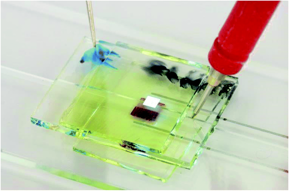 | ||
| Fig. 2 OLEC excitation and OPD detection system with a glass microfluidic device. For illustration reasons, the linear polarization filters are not integrated. The blue illuminating square is the illuminating blue OLEC pixel; the dark reds square is the active layer of OPD; the glass channel is in-between the OLEC and the OPD. | ||
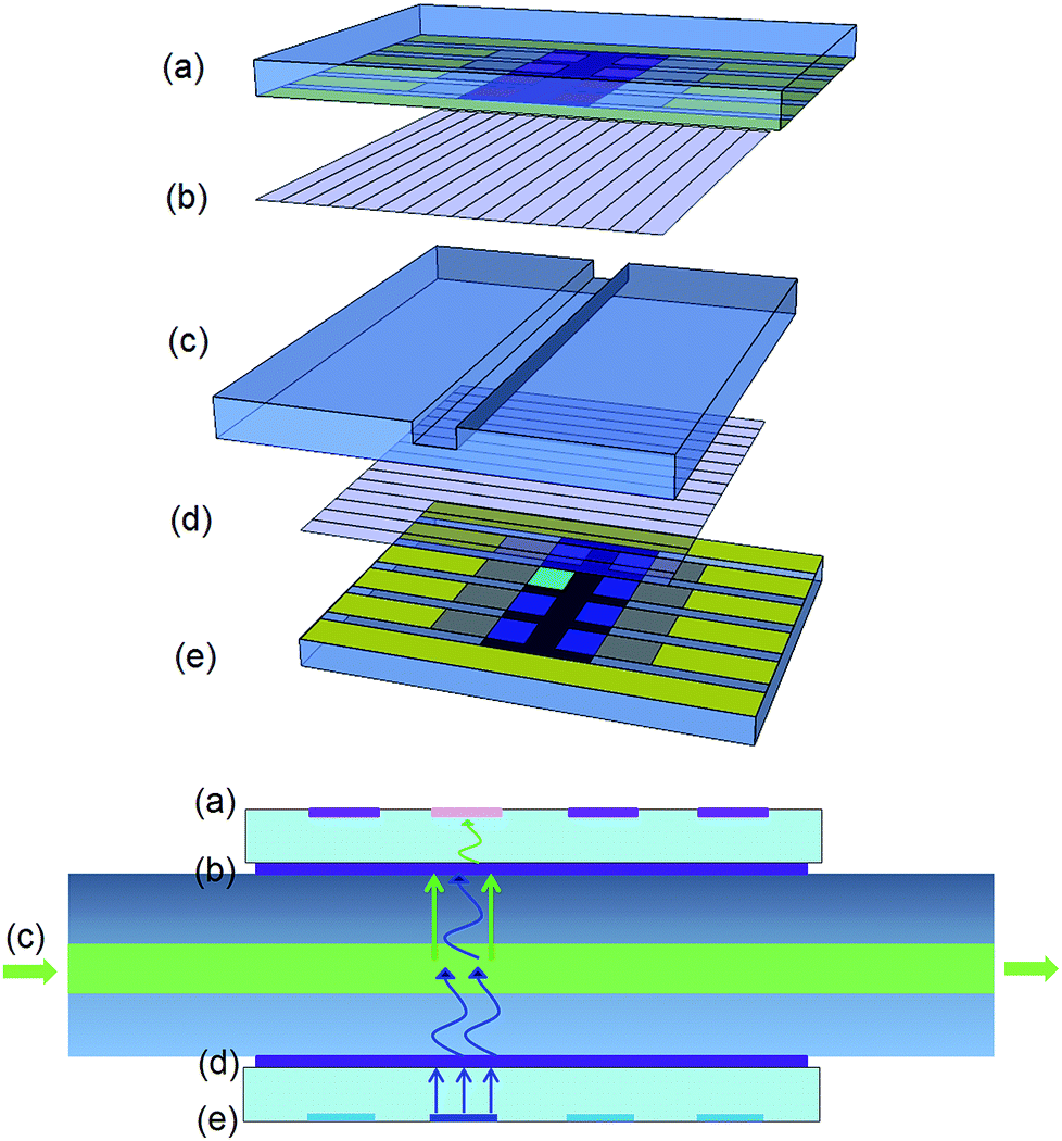 | ||
| Fig. 3 (top) Schematic exploded view and (bottom) 2D edge view of OLEC excitation and OPD detection system with a glass microfluidic device and polarization filters: (a) fully solution processed OPD; (b) first linear polarization filter oriented at 0 degree; (c) glass microfluidic chip; (d) second linear polarization filter oriented at 90 degree; (e) fully solution processed blue OLEC. | ||
Different concentrations of the fluorescent dye FAM were dissolved into distilled water and injected into the channel for fluorescent sensing testing. A HAMEG HMP2020 power supply (HAMEG Instruments GmbH) was used to generate voltage pulses for driving the OLECs, while a Trek Model 2210 power amplifier (Trek, Inc.) was combined with the power supply to supply voltage pulses. A Keithley model 6485 pico-amperemeter (purchased from Tektronix, Inc.) with a custom LabVIEW program was used to measure the photocurrent of the OPD. The brightness of the blue OLEC was measured by a calibrated silicon photodiode with an eye filter. The electroluminescent spectra were measured by an optical fiber coupled calibrated spectrometer (SD2000, Ocean Optics Inc., wavelength resolution of 2 nm).
Results and discussion
Organic light-emitting electrochemical cells
Organic light-emitting electrochemical cells can overcome the work-function mismatch by in situ electrochemical doping and ion redistribution (in situ generated PN-junction). However, this in situ doping leads to slow turn-on (the time required to emit 1 cd m−2 after applying electrical potential). Thanks to the low ionic mobility at room temperature and high ionic mobility at elevated temperature (>60 °C) of the crown ether electrolyte (DCH18C6),47 the in situ generated PN-junction can be pre-generated at elevated temperature and frozen at room temperature. Consequently, the pre-doped OLEC device shows a fast turn on and then can be operated at pulse mode to achieve higher emitted light brightness.As illustrated in Fig. 4, the fully solution processed blue OLEC shows relatively low brightness at low driving voltage (<15 V), however much higher brightness can be realized at higher voltage pulses. The emission brightness is dramatically increased after being pulsed at voltages higher than 20 V. Brightness more than 2800 cd m−2 can be achieved when the blue OLEC is pulse driven at 50 V. OLECs are known to have relatively short lifetimes due to the additional electrolyte and dopants.48–50 For disposable on-chip fluorescent sensing platforms, a sufficient lifetime of the excitation light source is required. Self-heating is one major degradation factor for organic light sources,51 thus a pulse driving with a low duty cycle can dramatically reduce the self-heating effect. Further thermal management50 can be implemented if more intense and fast measurements are demanded. The lifetime characterization of the pulsed blue OLEC shows that even when the device was operated at a high voltage to emit at a brightness as high as >2800 cd m−2, no degradation was observed after 10000 pulses. Even after 30000 pulses, 85% of original brightness can be still emitted.
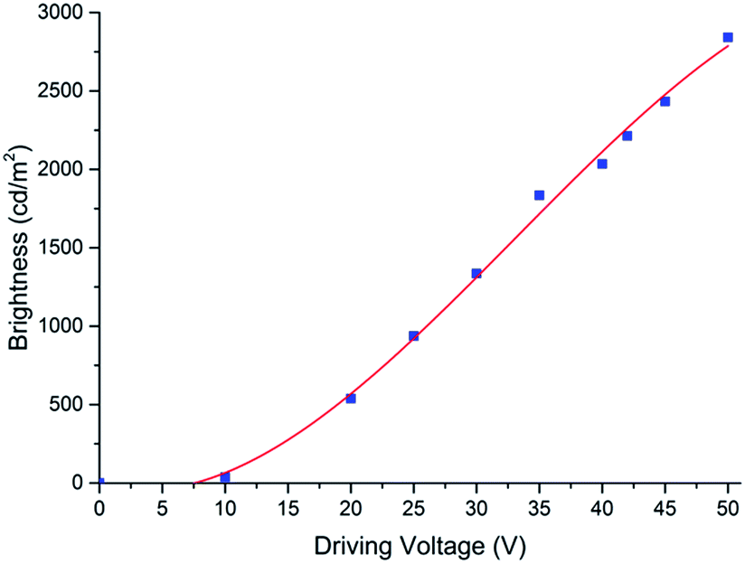 | ||
| Fig. 4 Driving voltage – brightness characterization of the fully solution processed blue OLEC, measured at voltage pulse mode (30 ms pulse width, 1% duty cycle). | ||
One advantage of using OLEDs and OLECs as a fluorescent sensing excitation light source is that the emission peak wavelength can be relatively easy tuned by via selecting different light emitting polymers or small molecules. However, the layer structure of OLEDs has to be slightly modified, e.g. a different electron transporting layer, when emitting a different light color via different emitters due to different energy band gaps. OLECs have the advantage of keeping exactly the same layer structure for different emitted colors due to the in situ doping mechanism. This provides great benefits in integrating several fluorescent sensing applications into one microfluidic chip via exactly the same, simple, and low-cost fabrication methods. In this paper, a blue emitter emitting in the range of 450 to 485 nm was chosen for demonstration due to its wide applications in chemical or biological fluorescent sensing. Fig. 5 illustrates the normalized emitted light spectrum of the fully solution processed blue OLEC and the absorption spectrum of the fluorescent dye FAM. It can be clearly seen that the absorption wavelength range of FAM fluorescent dye is well overlapped with blue OLEC emission light, and therefore this blue OLEC is a suitable light source for FAM fluorescent excitation.
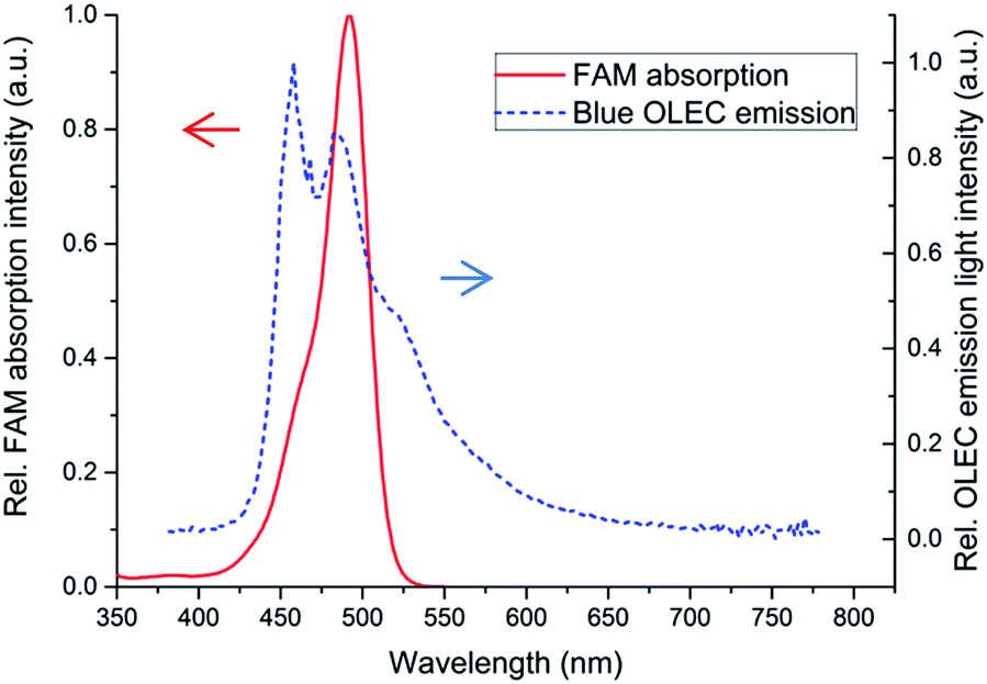 | ||
| Fig. 5 Emission spectrum of fully solution processed blue OLEC and the absorption spectrum of FAM. | ||
Organic photodiodes
An OPD was fabricated according to the parameters described in the experimental section. Fig. 6 shows the absorption spectrum of the active material used within the OPD. The P3TH:PCBM blend absorbs in a broad spectral range from 350 to 650 nm, due to the PCBM absorption from 350 to 450 nm and the P3HT absorption from 450 to 650 nm. However, the charge carriers contributing to the detectable photo current are only generated within the P3HT, limiting the detectable spectral range. The emission spectra of the selected fluorescent dye FAM is entirely covered by the absorption spectra of the OPD. At the maximum FAM emission peak at 518 nm the OPD shows a sensitivity of 0.11 A W−1 while the dark current density at 0 V was lower than 10 pA mm−2.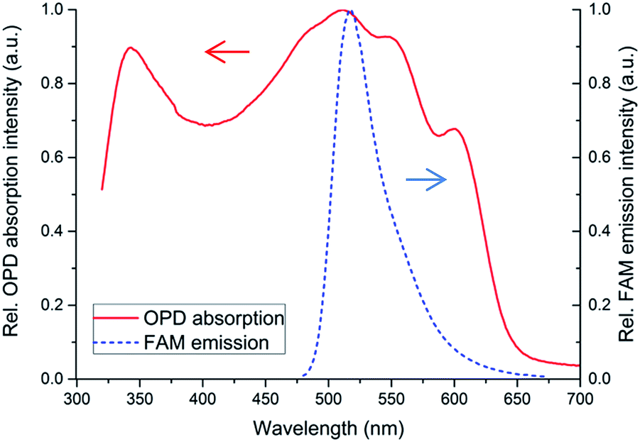 | ||
| Fig. 6 Absorption spectrum of fully solution processed blue organic photodiode and the emission spectrum of FAM. | ||
The wide spectral detection range of the OPD makes it compatible with many different fluorescent dyes. However, the combination with the wide emission range of the OLEC causes wide spectral overlap of OLEC and OPD (see Fig. 5 and 6). In addition, the fluorescent light intensity is orders of magnitude lower than the emitted light of the OLEC and not all of the OLEC light is absorbed by the FAM.52 Therefore, polarization filters are included into the chip. These filters can transmit polarized light within the full visible light spectrum. They are included on each side of the channel and with 90° rotation. Thus, no light of the OLEC should pass through the second filter.
Characterization of the fluorescence sensor
The extinction property of the linear polarization filters was first characterized with a sky blue inorganic LED and a silicon photodiode. With a single linear polarization filter, only 41.3% light intensity can be transmitted. Since the excitation light has to pass the first filter and the fluorescent light has to pass the second filter and assuming 50% of the fluorescent light emitted from the FAM is emitted toward the detector, only ∼8% of the emitted fluorescent light will reach the detector. When the two linear polarization filters were aligned orthogonally to each other, merely 0.012% of the light can be transmitted. This corresponds to a nominal extinction ratio of 38.5 dB.The photocurrent response of the fully solution processed OPD for various FAM concentrations in water from 1 to 200 μM was measured in the integrated chip with filters as well as the fully solution processed blue OLEC. The blue OLEC was pulsed at 20 V and 40 V to emit a light brightness of ∼500 cd m−2 and ∼2000 cd m−2, respectively.
Fig. 7 shows the fluorescence signals at different FAM concentrations as a function over pulse duration, which were excited by OLEC with 140 ms 20 V voltage pulse and detected by the OPD. The current values of the OPD were measured every 20 ms which corresponds to six different measurement values for each light pulse. The background noise, which was measured using pure distilled water instead of FAM solution, was subtracted from the measurement values. It consists of the dark current of the OPD and the passing light from the blue OLEC through two orthogonally-oriented polarization filters. The measured background photocurrents for measurement with 500 cd m−2 and 2000 cd m−2 excitation light intensity was as low as 57 pA and 348 pA, respectively.
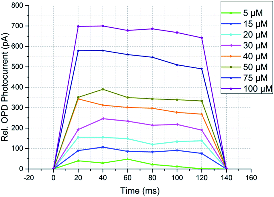 | ||
| Fig. 7 FAM fluorescence response measured with the OPD at different FAM concentrations. | ||
For all curves in Fig. 7 a gradual decrease in the measured current can be observed over time. This is related to the excitation light intensity of the OLEC used. OLECs tend to have a higher light intensity when turned on, while decreasing to a saturated value after few seconds. Therefore, for pulsed operation of the OLEC is preferred rather than continuous driving for measurements. To evaluate the dependency of the fluorescence response on the FAM concentration the 6 data points per light pulse were averaged. The results can be seen in Fig. 8a and b, respectively.
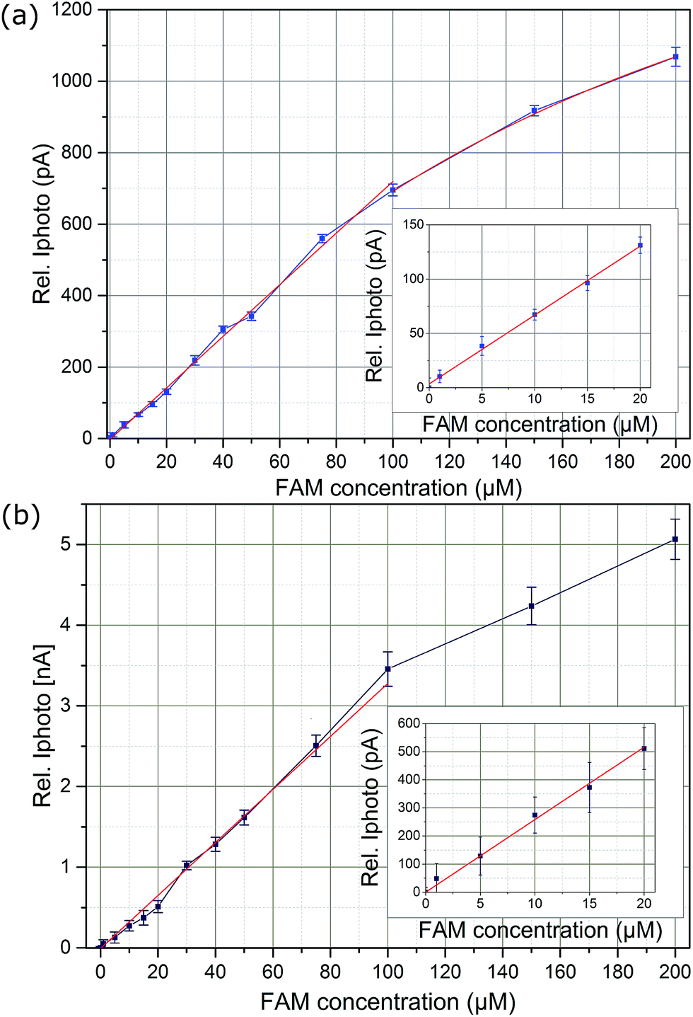 | ||
| Fig. 8 Fluorescent detection measurement by integrated OLEC and OPD with different FAM dye concentration in water. The FAM solution was excited by the blue OLEC with brightness of (a) 500 cd m−2 and (b) 2000 cd m−2; the inset graph is the zoom-in of the low concentration part (1 to 20 μM). | ||
The error bars present deviated measurement values from different OLEC pulses for each FAM concentration. As shown in Fig. 8b, there is a relatively high deviation of measured photocurrent over several OLEC pulses at a brightness of ∼2000 cd m−2. That is because 30 ms pulse width was used in order to avoid any influence of device degradation over the whole measurement. Moreover, the fluorescent light photocurrents were measured every 20 ms as indicated in Fig. 7. Alternative to use a high speed measurement setup, the measurement error can be reduced with longer excitation light pulses and taken the average value over the pulses. This strategy was used for the case with OLEC emission brightness of 500 cd m−2 and pulse-width of 140 ms, the deviation was highly reduced to less than 5% down to FAM concentration as low as 10 μM.
It can be observed that concentrations as low as 1 μM can be measured even with a relatively low brightness of 500 cd m−2 of the blue OLEC device, which corresponds to an OLEC electrical driving power as low as 5.8 mW. For low concentrations up to 20 μM, a strong linear dependency (R = 0.9999) is visible. This linear dependency could be extended to 100 μM. For concentrations of more than 100 μM both graphs for 500 cd m−2 and 2000 cd m−2 start to become non-linear with a decrease in the graphs slope. This non-linearity is an intrinsic behaviour of the intensity dependency of the fluorescence response itself.
The signal to noise (S/N) ratio was calculated and is presented in Fig. 9. When the measured photocurrent is close to the background noise, the measurement setup reaches its theoretical absolute limit of detection (LOD), i.e. S/N ratio equals 1. A S/N ratio of 1.1 (illustrated in Fig. 9, blue dash line) is a more practical measurement LOD, which in our case is about 500 nM. Based on this criteria, our device shows a better performance than the literature reports with more efficient evaporated OLED and OPD combinations.22,26 This demonstrates that solution processed OLECs and OPDs can be a suitable combination for the direct integration of a microfluidic fluorescent detection setup. Moreover, it brings the advantages of low cost, flexibility and direct on-chip integration.
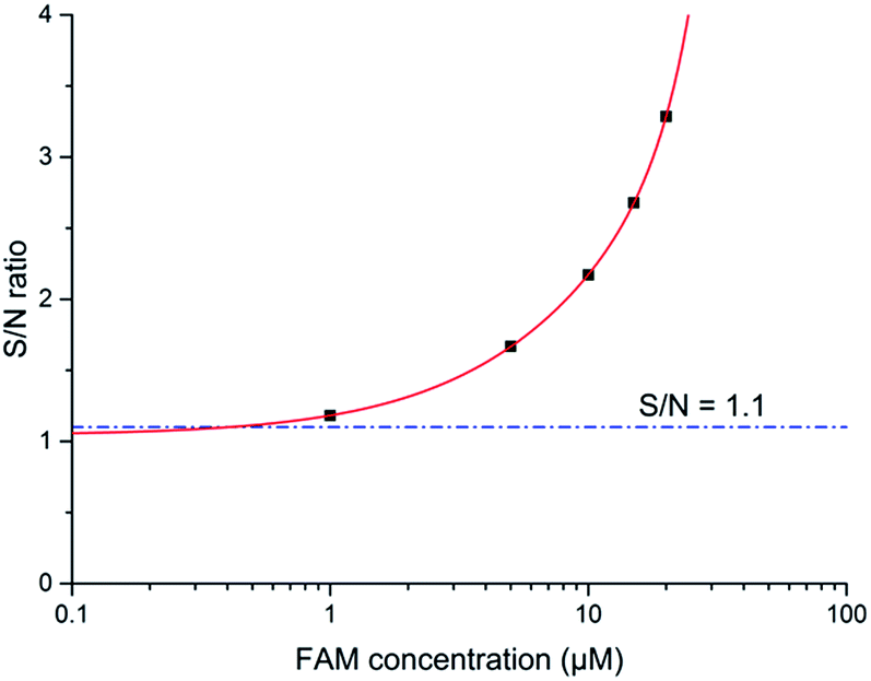 | ||
| Fig. 9 S/N ratio as a function of concentration of FAM dye as OLEC driven at 20 V pulses. Solid red line predicted trends for the theoretical LOD at S/N = 1.1, which is shown with a dashed blue line. | ||
Conclusions
We have demonstrated the first microfluidic fluorescent sensing system including both a fully solution processed light source and a fully solution processed photodetector. The blue OLEC is first introduced and demonstrated as a low-cost excitation light source. OLECs was fabricated with solution processing method. With additional doping material, the manufacturing of the OLEC is less critical on layer homogeneity and surface roughness. Moreover, the emission light peak can be relatively easily modified by selecting different light emitting polymers. In this demonstration, the peak wavelength of the selected blue light-emitting polymer was in the range of 450 to 485 nm, which is suitable to excite FAM fluorescent dyes. The OLEC showed a high brightness of up to 2800 cd m−2 at a driving voltage of 50 V. In pulsed operation the device was very stable and can survive for more than 10000 pulses without degradation. As a photodetector we manufactured an organic photodiode via fully solution processing. The diode shows broadband light absorption properties in the range of 450 to 650 nm. Therefore, the OPD is compatible with various fluorescent dyes such as the FAM in this demonstration. In order to separate the OPD from the fluorescence excitation light of the OLEC we included two orthogonally oriented linear polarizers into the microfluidic glass chip. At both 500 cd m−2 and 2000 cd m−2 OLEC brightness, minimum concentrations of as low as 1 μM FAM in water with a S/N-ratio > 1.1 could be detected. The low detection limit, the low power consumption and the possibility of detecting various fluorescent dyes make the demonstrated system suitable for various point of care applications. These results show that this fluorescence sensor featuring a combination of a fully solution processed OLEC and OPD, with linear polarization filters provides a viable solution for portable, disposable or multi-usage point-of-care applications.
Acknowledgements
The current work on solution processed and inkjet printed OLECs and OPDs for lab-on-chip fluorescence sensing systems is funded by the BMBF within the joint research project “HandyLoC” (FKZ 13N13717) and managed by VDI Technologiezentrum. We would like to thank Mr Ben Zaage for developing the LabVIEW program to record the OPD photocurrents and Dr Rossá Mac Ciarnáin for the OLEC electroluminescent spectrum measurement.References
- C. D. Chin, V. Linder and S. K. Sia, Lab Chip, 2012, 12, 2118–2134 RSC.
- C. D. Chin, V. Linder, S. K. Sia, A. S. Daar, H. Thorsteinsdottir and D. K. Martin, Lab Chip, 2007, 7, 41–57 RSC.
- A. St John and C. P. Price, Clin. Biochem. Rev., 2014, 35, 155–167 Search PubMed.
- Lab a Chip Blog, 2015.
- P. Tseng, C. Murray, D. Kim and D. Di Carlo, Lab Chip, 2014, 14, 1491 RSC.
- J. Li, F. Rossignol and J. Macdonald, Lab Chip, 2015, 15, 2538–2558 RSC.
- O. Pabst, J. Perelaer, E. Beckert, U. S. Schubert, R. Eberhardt and A. Tünnermann, Organic Electronics physics materials applications, 2013, 14, 3423–3429 CAS.
- O. Pabst, S. Hölzer, E. Beckert, J. Perelaer, U. S. Schubert, R. Eberhardt and A. Tünnermann, Organic Electronics physics materials applications, 2014, 15, 3306–3315 CAS.
- E. Beckert, R. Eberhardt, O. Pabst, F. Kemper, Z. Shu, A. Tünnermann, J. Perelaer, U. Schubert and H. Becker, Proc. SPIE, 2013, 86150E CrossRef.
- C. Hoera, M. M. Skadell, S. A. Pfeiffer, M. Pahl, Z. Shu, E. Beckert and D. Belder, Sens. Actuators, B, 2016, 225, 42–49 CrossRef CAS.
- C. Hoera, S. Ohla, Z. Shu, E. Beckert, S. Nagl and D. Belder, Anal. Bioanal. Chem., 2015, 407, 387–396 CrossRef CAS.
- T.-a. Meier, E. Poehler, F. Kemper, O. Pabst, H.-G. Jahnke, E. Beckert, A. Robitzki and D. Belder, Lab Chip, 2015, 15, 2923–2927 RSC.
- R. Fobel, A. E. Kirby, A. H. C. Ng, R. R. Farnood and A. R. Wheeler, Adv. Mater., 2014, 26, 2838–2843 CrossRef CAS.
- H. Ko, J. Lee, Y. Kim, B. Lee, C.-H. H. Jung, J.-H. H. Choi, O.-S. S. Kwon and K. Shin, Adv. Mater., 2014, 26, 2335–2340 CrossRef CAS.
- K. Maejima, T. Enomae, A. Isogai, K. Suzuki and D. Citterio, in NIP28: International Conference on Digital Printing Technologies and Digital Fabrication, 2012, pp. 554–556 Search PubMed.
- Y. Guo, L. Li, F. Li, H. Zhou and Y. Song, Lab Chip, 2015, 15, 1759–1764 RSC.
- H. Gai, Y. Li and E. S. Yeung, in Top Curr Chem, 2011, pp. 171–201 Search PubMed.
- F. B. Myers and L. P. Lee, Lab Chip, 2008, 8, 2015–2031 RSC.
- G. Meller, T. Grasser, in Advances in Polymer Science, ed. T. Grasser, G. Meller and L. Li, Springer, Berlin, Heidelberg, 2010, vol. 223, pp. 45–71.
- S. R. Forrest, Nature, 2004, 428, 911–918 CrossRef CAS.
- R. Liu, Y. Cai, J.-M. Park, K.-M. Ho, J. Shinar and R. Shinar, Adv. Funct. Mater., 2011, 21, 4744–4753 CrossRef CAS.
- A. Pais, A. Banerjee, D. Klotzkin and I. Papautsky, Lab Chip, 2008, 8, 794–800 RSC.
- K. S. Shin, Y. H. Kim, K. K. Paek, J. H. Park, E. G. Yang, T. S. Kim, J. Y. Kang and B. K. Ju, IEEE Electron Device Lett., 2006, 27, 746–748 CAS.
- F. Lefèvre, A. Chalifour, L. Yu, V. Chodavarapu, P. Juneau and R. Izquierdo, Lab Chip, 2012, 12, 787–793 RSC.
- Y. Shuai, A. Banerjee, D. Klotzkin and I. Papautsky, Proc. IEEE Sensors, 2008, pp. 122–125 Search PubMed.
- G. Williams, C. Backhouse and H. Aziz, Electronics, 2014, 3, 43–75 CrossRef.
- E. M. Lindh, A. Sandstroem and L. Edman, Small, 2014, 10, 4148–4153 CrossRef CAS.
- A. Verma, D. M. Zink, C. Fléchon, J. L. Carballo, H. Flügge, J. M. Navarro, T. Baumann and D. Volz, Appl. Phys. A, 2016, 122, 191 CrossRef.
- L. Derue, S. Olivier, D. Tondelier, T. Maindron, B. Geffroy and E. Ishow, ACS Appl. Mater. Interfaces, 2016, 8, 16207–16217 CrossRef CAS.
- Q. Pei, G. Yu, C. Zhang, Y. Yang, A. J. Heeger, A. J. H. Qibing Pei, G. Yu, C. Zhang and Y. Yang, Science, 1995, 269, 1086–1088 CrossRef CAS.
- A. Asadpoordarvish, A. Sandström, C. Larsen, R. Bollström, M. Toivakka, R. Österbacka and L. Edman, Adv. Funct. Mater., 2015, 25, 3238–3245 CrossRef CAS.
- Z. Shu, O. Pabst, E. Beckert, R. Eberhardt and A. Tünnermann, Mater. Today, 2016, 3, 733–738 Search PubMed.
- Z. Shu, O. Pabst, E. Beckert, R. Eberhardt and A. Tünnermann, in SPIE 9745, Organic Photonic Materials and Devices XVIII, ed. C. E. Tabor, F. Kajzar, T. Kaino and Y. Koike, International Society for Optics and Photonics, San Francisco, California, United States, 2016, p. 97450W Search PubMed.
- F. Zhang, D. Wu, Y. Xu and X. Feng, J. Mater. Chem., 2011, 21, 17590 RSC.
- H. Zhou, L. Yang and W. You, Macromolecules, 2012, 45, 607–632 CrossRef CAS.
- S. Bai, Z. Wu, X. Xu, Y. Jin, B. Sun, X. Guo, S. He, X. Wang, Z. Ye, H. Wei, X. Han and W. Ma, Appl. Phys. Lett., 2012, 100, 203906 CrossRef.
- S. Albrecht, S. Janietz, W. Schindler, J. Frisch, J. Kurpiers, J. Kniepert, S. Inal, P. Pingel, K. Fostiropoulos, N. Koch and D. Neher, J. Am. Chem. Soc., 2012, 134, 14932–14944 CrossRef CAS.
- M. Binda, A. Iacchetti, D. Natali, L. Beverina, M. Sassi and M. Sampietro, Appl. Phys. Lett., 2011, 98, 73303 CrossRef.
- A. Armin, R. D. Jansen-van Vuuren, N. Kopidakis, P. L. Burn and P. Meredith, Nat. Commun., 2015, 6, 6343 CrossRef CAS.
- A. Llobera, S. Demming, H. N. Joensson, J. Vila-Planas, H. Andersson-Svahn and S. Büttgenbach, Lab Chip, 2010, 10, 1987–1992 RSC.
- C. Richard, A. Renaudin, V. Aimez and P. G. Charette, Lab Chip, 2009, 9, 1371–1376 RSC.
- J. G. Cuennet, A. E. Vasdekis and D. Psaltis, Lab Chip, 2013, 13, 2721–2726 RSC.
- T. Arii and A. Kishi, J. Therm. Anal. Calorim., 2006, 83, 253–260 CrossRef CAS.
- P. de Bruyn, D. J. D. Moet and P. W. M. Blom, Org. Electron., 2010, 11, 1419–1422 CrossRef CAS.
- C. Do Park, T. A. Fleetham, J. Li and B. D. Vogt, Organic Electronics physics materials applications, 2011, 12, 1465–1470 CrossRef.
- H. Kim, W. W. So and S. J. Moon, J. Korean Phys. Soc., 2006, 48, 441–445 CAS.
- G. Yu, Y. Cao, M. Andersson, J. Gao and A. J. Heeger, Adv. Mater., 1998, 10, 385–388 CrossRef CAS.
- S. Tang and L. Edman, J. Phys. Chem. Lett., 2010, 1, 2727–2732 CrossRef CAS.
- J. Fang, P. Matyba and L. Edman, Adv. Funct. Mater., 2009, 19, 2671–2676 CrossRef CAS.
- Y. Zhang and J. Gao, J. Appl. Phys., 2006, 100, 84501 CrossRef.
- T. Wågberg, P. R. Hania, N. D. Robinson, J.-H. H. Shin, P. Matyba and L. Edman, Adv. Mater., 2008, 20, 1744–1749 CrossRef.
- A. Sharma and S. G. Schulman, Introduction to Fluorescence Spectroscopy, Wiley, 1999 Search PubMed.
Footnote |
| † These authors contributed equally for this work. |
| This journal is © The Royal Society of Chemistry 2017 |