
 Open Access Article
 This Open Access Article is licensed under a
 Creative Commons Attribution 3.0 Unported Licence
Effects of electrochemical reaction and surface morphology on electroactive surface area of porous copper manufactured by Lost Carbonate Sintering†
Pengcheng
Zhu
 * and
Yuyuan
Zhao
* and
Yuyuan
Zhao
School of Engineering, University of Liverpool, Liverpool L69 3GH, UK. E-mail: sgpzhu@liverpool.ac.uk; Tel: +44 0 7709606856
First published on 17th May 2017
Abstract
Porous metals are potentially excellent electrode materials because of their high specific surface areas. The electroactive surface area is dependent on the electrochemical reaction and can be affected by the surface morphology. This work measured the electroactive surface area of porous Cu manufactured by the Lost Carbonate Sintering process, using the cyclic voltammetry (CV) peak current method and employing two reactions with different Nernst diffusion layer thicknesses. The real surface area was also measured by the double layer capacitance method. The effects of Cu particles size, sintering temperature and chemical treatment on the surface morphology and therefore surface areas were investigated. Cu particle size had a modest effect, with the medium particle sizes, 20–45 μm or 45–75 μm, showing the highest surface areas. Increasing the sintering temperature from 850 °C to 950 °C or etching the samples by 5 M nitric acid for 5 minutes reduced the electroactive and real surface areas by 31–61% or 9–25%, respectively. The electroactive surface area was increased by up to 2 times when the diffusion layer thickness was decreased from 50 μm to 1 μm.
1. Introduction
Open-cell porous metals are potentially excellent electrode materials in energy generation and storage due to their unique combinations of material and structural characteristics.1 Their applications include lithium-ion battery,2,3 alkaline zinc battery,4 nickel–hydrogen battery,5 solid oxide fuel cell6,7 and electrochemical capacitor.8 The performance of porous electrodes depends strongly on the magnitude of their specific surface area, because a higher specific surface area offers more reaction sites for reactants or a larger storage capacity for electrons per unit volume of electrodes, generating a higher energy density. Characterisation of surface area is therefore essential, especially for porous electrodes. The surface area of a number of porous metals manufactured by different processes, including porous Ni9,10 and Au,11 have been measured by BET. However, the active surface area of porous electrodes has been found to be sensitive to the electrochemical process involved.12Diao et al.12 developed a cyclic voltammetry (CV) peak current method to measure the electroactive surface area of porous copper manufactured by a space holder process, based on the principle that the anodic or cathodic peak current for a diffusion controlled reaction is proportional to the electroactive surface area of the electrode.13 They chose the predominant anodic current peak and used a series of polished copper plates with known surface areas to establish the quantitative relation between electroactive surface area and peak current for copper. Using this quantitative relation, the electroactive surface area of a series of porous Cu samples with different pore sizes and porosities was determined from the measured peak current. In their work, however, the other current peaks in the cyclic voltammograms were not considered. Several questions then arise. Can other current peaks also be used for electroactive surface area measurements? If they can, would they measure a different electroactive surface area? What is the key factor causing the difference?
The electroactive surface area measured by the CV peak current method is expected to be reaction-dependent, because different reactions may be controlled by the diffusion of different reactant species. The Nernst diffusion layer determines the regime of the diffusion in a porous electrode and will have an influence on the electroactive surface area ref. 9. There are two diffusion regimes, depending on the thickness of the Nernst diffusion layer relative to the size of the interstices in the porous structure.14–17 If the diffusion layer is thinner than the size of the interstices, semi-infinite diffusion occurs. If the diffusion layer is comparable to or greater than the interstices, then thin layer diffusion occurs. A porous electrode is expected to contribute more to the detectable electroactive surface area with a thinner Nernst diffusion layer. Using different reactions in the CV peak current method will provide a powerful tool not only to measure surface areas at different length scales but also to study the effect of surface morphology on the surface area of porous metals.
It is well known that the surface area of porous metals is very sensitive to the surface morphology.18–20 Campell and Bakker21 electrodeposited a mesoporous nickel film onto a common porous nickel and founded that the surface area was increased by up to 35 times. Grdeń et al.18 compared INCO porous nickel before and after nitric acid etching and showed that the etching increased the electroactive surface area by about 150% because of increased surface roughness. Tan et al.19 reported that the surface area of a nanoporous gold was decreased by up to 3.5 times when it was annealed at 400 °C, because the annealing flattened the surface. However, very little research, apart from ref. 10, has been carried out to date on the surface area of porous metals manufactured by powder metallurgy based methods and even less on how the surface area is affected by thermal and chemical treatments.
In this paper, we studied the surface areas of porous copper manufactured by the Lost Carbonate Sintering (LCS) process.22,23 The porous metal samples manufactured by the LCS process have representative porous structure produced by the powder metallurgy based space-holder methods, with highly-controllable porosity, pore size and pore shape. Two electrochemical reactions with different Nernst diffusion layer thicknesses were employed to measure the electroactive surface area using the CV peak current method. The real surface area was measured by the double layer capacitance method. The pore surface morphology of the LCS porous copper was modified by using different copper particle sizes, sintering conditions and chemical etching, and their effects on the electroactive and real surface areas were investigated.
2. Experimental
2.1 Preparation of porous copper samples
Porous Cu samples with different pore sizes and porosities were manufactured by the LCS process,22 as shown schematically in Fig. 1. The raw materials were commercially pure Cu powder (Ecka Granules Metal Powder Ltd., Wednesdbury, UK) and food grade K2CO3 powder (E&E Ltd., Melbourne, Australia). The Cu powder had spherical particles and was sieved into four different ranges of particle sizes: <20 μm, 20–45 μm, 45–75 and 75–90 μm. The K2CO3 powder had rounded particles with a particle size range of 1000–1500 μm. The Cu and K2CO3 powders were mixed with an intended volume fraction of Cu according to the target porosity. The mixture was compacted at 200 MPa by a hydraulic press. The obtained preform was then sintered in a vacuum furnace. Two different sintering temperatures were used to effect different surface morphologies. A group of the preforms were sintered at 850 °C for 4 hours and the K2CO3 particles were subsequently removed by dissolution in hot water. The other group of preforms were sintered at 950 °C for 2 hours and the K2CO3 particles were removed by decomposition during the sintering. The as-produced porous copper samples were cut to a uniform size of 5 mm × 5 mm × 4.8 mm by an electrical discharge machine (Prima E250, ONA Ltd., Bristol, UK), see ESI Fig. S1.† The morphology of the LCS porous Cu samples was observed by a scanning electron microscope (JSM-6610, Japan).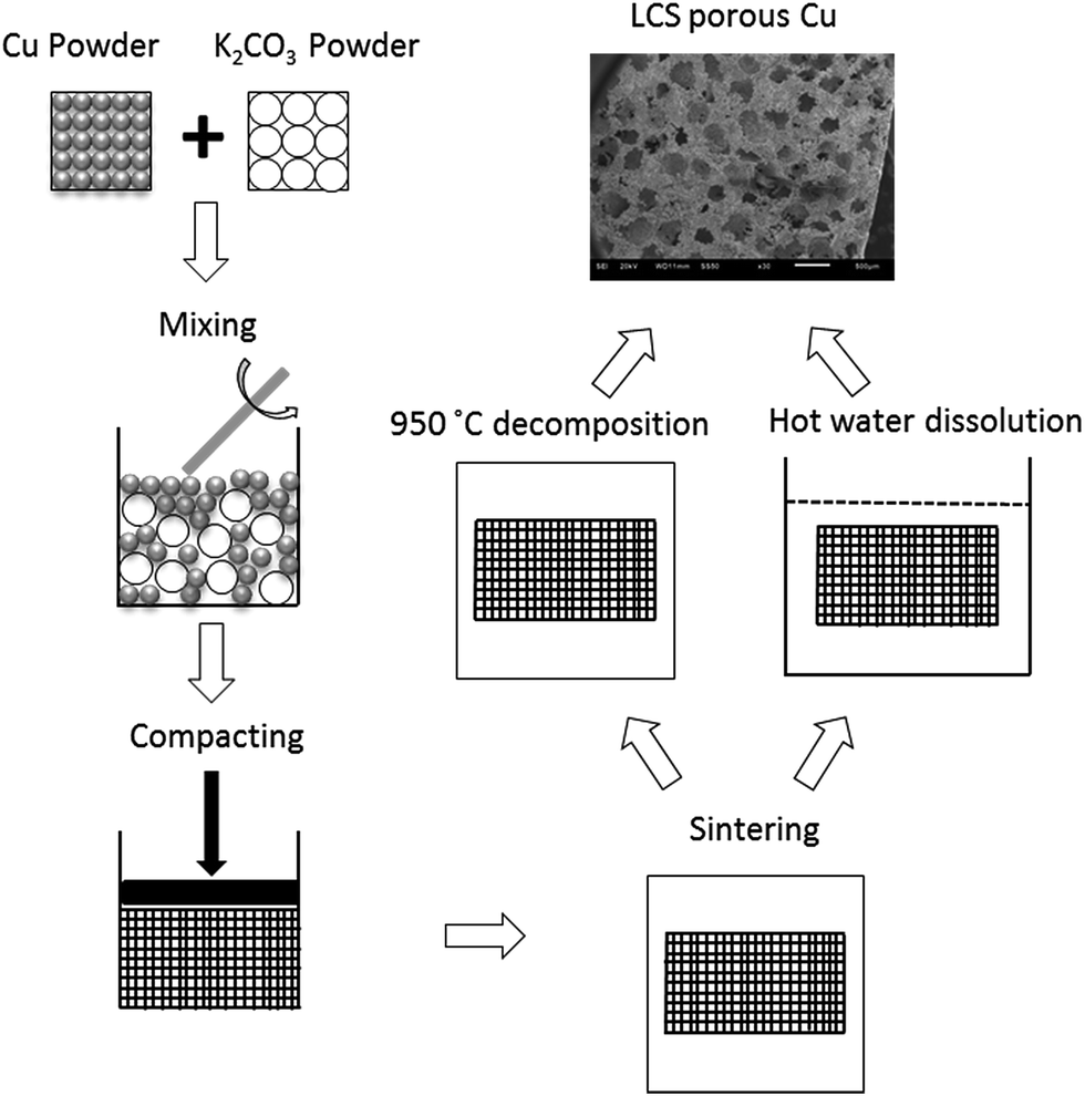 | ||
| Fig. 1 Schematic of the LCS process for manufacturing porous Cu. | ||
2.2 Chemical etching
The as-produced porous Cu samples were ultrasonically cleaned in dilute hydrochloric acid to remove the copper oxide on the surface and then washed with distilled water. The samples were subsequently chemically etched and the electroactive and real surface areas were measured both before and after etching. The etching treatment was carried out by immersing the samples in 5 M nitric acid under ultrasonication at room temperature for 5 minutes. The weight loss of the etched samples was less than 5%. Samples with porosities higher than 70% were not etched, because etching could easily result in a weight loss higher than 10% and therefore significant changes in the porous structure.2.3 Electrochemical surface area measurement
The electroactive surface area measurement of the LCS porous Cu was carried out following a similar procedure reported in.12Fig. 2a shows a typical current–potential plot of the porous Cu samples in 0.1 M KOH solution in the potential range of −1.6 to 0.7 V at a scan rate of 0.01 V s−1, which had a similar shape as that of a solid Cu electrode but with a different magnitude (see ESI Fig. S2†). There are two current peaks in the forward sweeping part of the curve. The peaks, 1 and 2, indicate two different chemical reactions, (1) and (2), respectively:24,25| 2Cu + 2OH− → Cu2O + H2O + 2e | (1) |
| Cu + 2OH− → Cu(OH)2 + 2e | (2) |
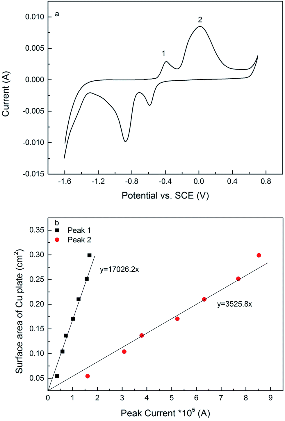 | ||
| Fig. 2 (a) Typical current–potential plot of porous copper in 0.1 M KOH in the potential range of −1.6 to 0.7 V at a scan rate of 0.01 V s−1. (b) Linear relations between peak current and surface area for mirror polished copper plates. | ||
Reactions (1) and (2) were controlled by the diffusion of Cu+ in the solid electrode and the diffusion of OH− in the electrolyte, respectively.24,25 Both reactions were used to measure the electroactive surface areas with an aim to study the effects of the chosen reaction and the diffusion layer thickness.
Seven copper plates with known geometric surface areas were used to determine the relations between peak current and surface area for copper (see ESI Fig. S3†). The copper plates were ground by sandpapers (grits 80, 320, 600 and 1200), polished by cloths (6 and 1 μm) and further polished by a silk-type cloth pad with a 0.04 μm colloidal silica suspension to achieve a mirror finish. The electroactive surface areas of the copper plates can be regarded as equal to their geometric surface areas. Fig. 2b shows that there are linear relations between peak current and surface area for both peaks 1 and 2, and the relations can be expressed quantitatively by:
| A1 = 17026.2Ip1 | (3) |
| A2 = 3525.8Ip2 | (4) |
The effect of electrolyte resistance, which was not mentioned in ref. 9, was considered in this work. The high surface area of the porous copper resulted in currents in the order of 10 mA when 0.1 M KOH was used. The high currents can cause significant distortions in the voltammetry if the solution resistance is not compensated.17 To this end, the “IR-compensation” feature in the potentiostat was used to automatically compensate the potential signal for solution resistance for porous samples. The compensation of solution resistance was not necessary for copper plates, because of the low current density generated.
The real surface area of the porous Cu samples was measured by the double layer capacitance method, following the procedure reported in.12 The double layer capacitance of the LCS porous copper was determined from the charge/discharge current (eqn (5)).26 Because the specific capacitance for the interface of copper in 0.1 M KOH solution is 0.02 mF cm2,27 the real surface area of the porous copper can be determined by eqn (6):
 | (5) |
 | (6) |
3. Results and discussions
3.1 Morphology of the LCS porous copper
Fig. 3 shows the SEM images of the LCS porous Cu samples manufactured with different Cu particle sizes and different sintering and chemical treatment conditions. The samples sintered at 850 °C (first row) have rough surfaces, with the initial spherical Cu particles easily discernible. It can also be observed that the smaller the Cu particles, the thicker the sintering necks relative to the particle size. The samples sintered at 850 °C and etched (second row) show smoother surfaces, revealing strong sintering necks and making original particles less visible, especially in the small Cu particle sample (Fig. 3E). The samples sintered at 950 °C (third row) are apparently denser and have thicker sintering necks than the samples sintered at 850 °C (first row) for any given Cu particle size. The sample made from the smallest particles (Fig. 3I) is fully sintered with the original particles barely discernible. The original particles can still be seen in the samples made form larger particles (Fig. 3J–L), but they are less noticeable than in the samples sintered at 850 °C (first row). The samples sintered at 950 °C and subsequently etched (fourth row) show more flat surfaces, with the original particles hardly noticeable for all samples.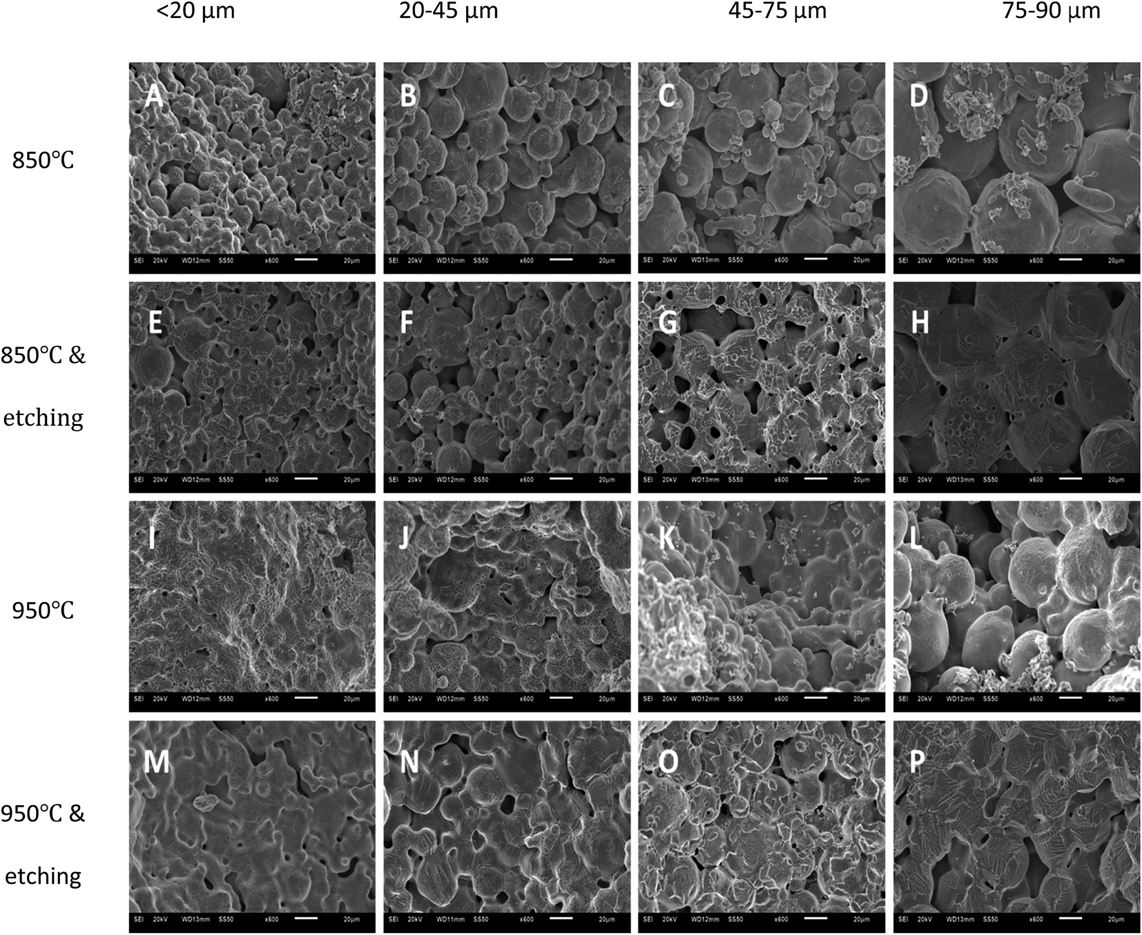 | ||
| Fig. 3 SEM images of the LCS porous Cu samples with different Cu particle sizes and processing conditions. | ||
3.2 Effect of particle size on surface areas
The volumetric electroactive surface areas, measured by the diffusion of Cu+ (ACu+) and OH− (AOH−), and the volumetric real surface area (Ar) of the LCS porous Cu samples with different particle sizes and porosities, manufactured under different process conditions, are shown in Fig. 4–6, respectively. All data are also available in ESI Tables S1–S3.† It is obvious that the surface areas are affected by both Cu particle size and porosity for all manufacturing and treatment conditions. For each process condition, the surface areas vary with porosity without any particular pattern, in agreement with.12 In order to remove the effect of porosity and focus on the effect of particles size, the average volumetric electroactive surface area for each particle size is also shown in the graphs. Fig. 4–6 show that Cu particle size has a moderate effect on the electroactive and real surface areas. As a general trend, both the electroactive surface areas (Fig. 4 and 5) and the real surface area (Fig. 6) first increase and then decrease with particle size. The maximum surface area values are achieved in the samples either with a particle size of 20–45 μm or with a particle size of 45–75 μm.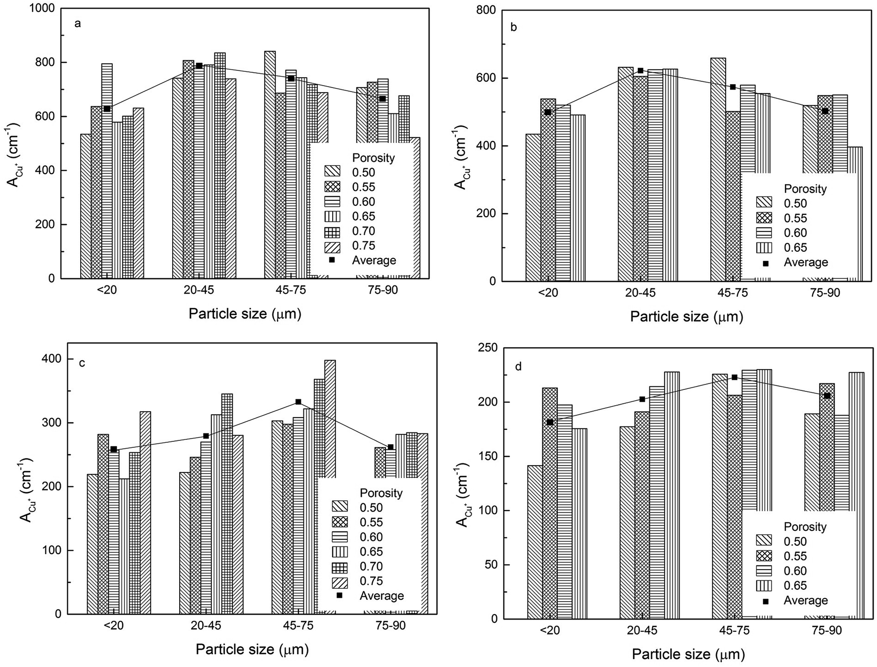 | ||
| Fig. 4 Volumetric electroactive surface area, measured by the diffusion of Cu+, of the LCS porous Cu samples with different particle sizes for different porosities, manufactured by (a) 850 °C sintering, (b) 850 °C sintering and etching, (c) 950 °C sintering and (d) 950 °C sintering and etching. | ||
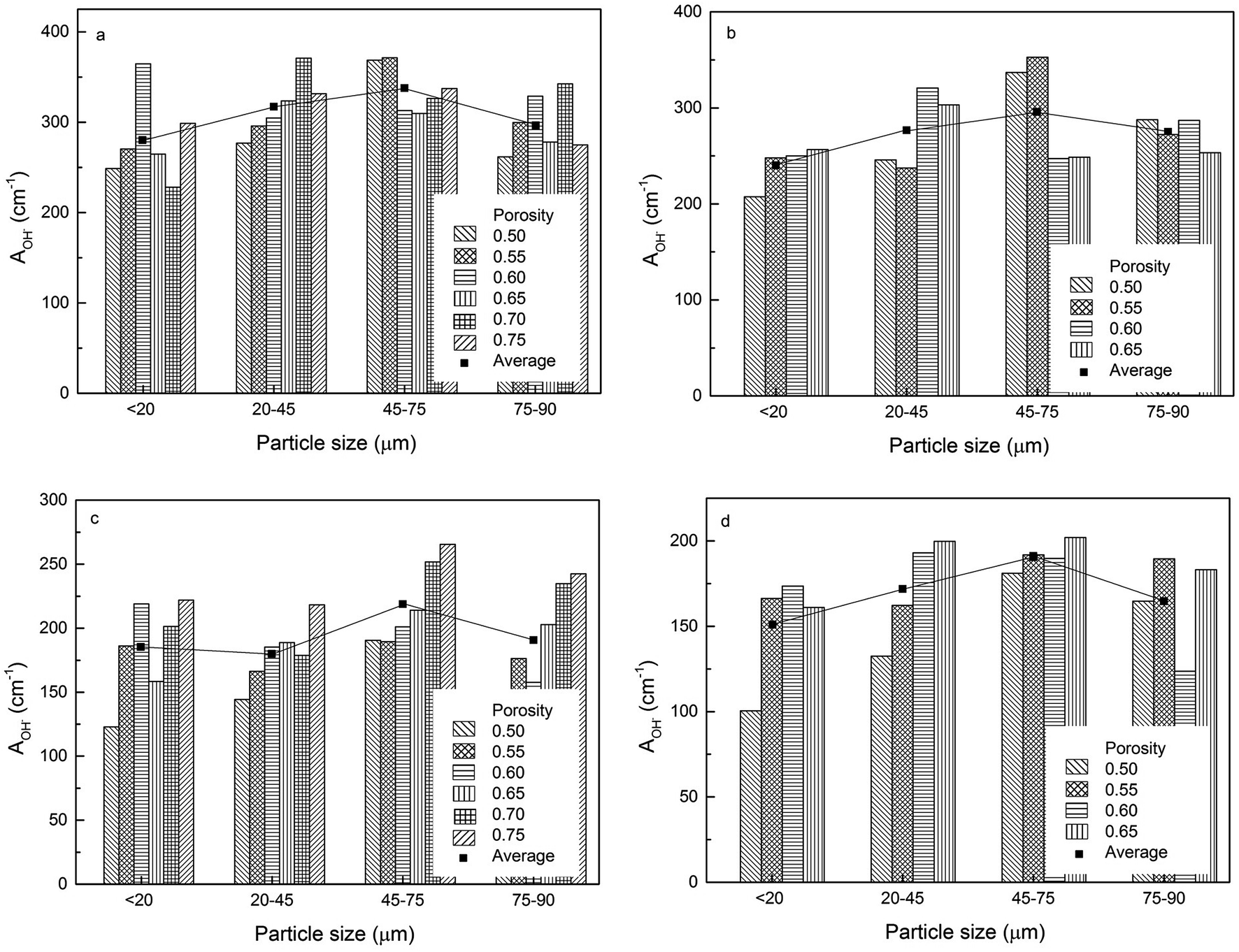 | ||
| Fig. 5 Volumetric electroactive surface area, measured by the diffusion of OH−, of the LCS porous Cu samples with different particle sizes for different porosities, manufactured by (a) 850 °C sintering, (b) 850 °C sintering and etching, (c) 950 °C sintering and (d) 950 °C sintering and etching. | ||
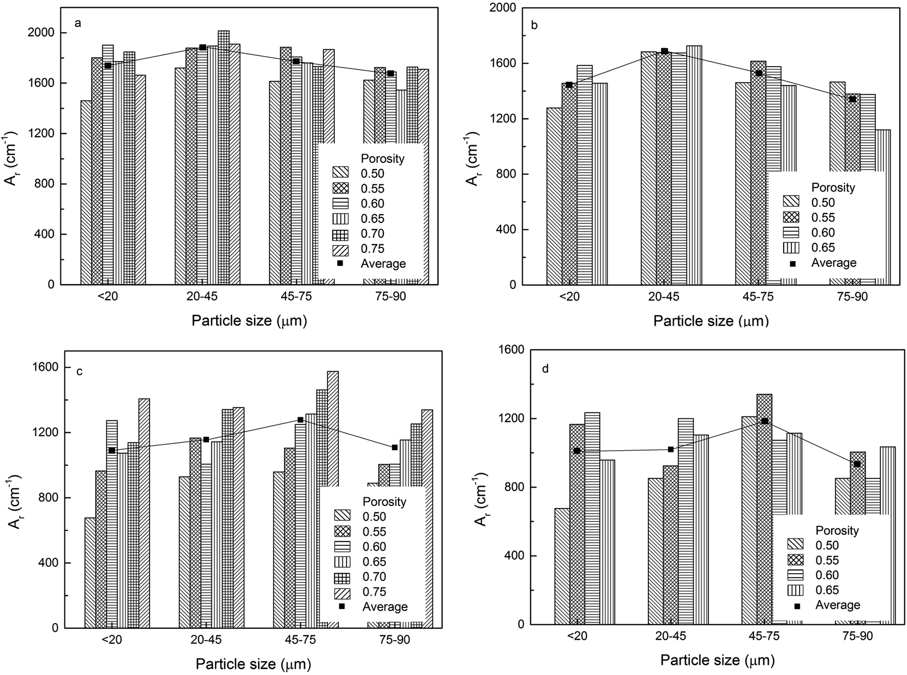 | ||
| Fig. 6 Volumetric real surface area of the LCS porous Cu samples with different particle sizes for different porosities, manufactured by (a) 850 °C sintering, (b) 850 °C sintering and etching, (c) 950 °C sintering and (d) 950 °C sintering and etching. | ||
The effect of Cu particle size on surface area is twofold. On the one hand, smaller particles offer a higher total surface area.12 On the other hand, it is easier to sinter smaller particles to achieve a denser structure, resulting in a huge loss in surface area. In contrast, larger Cu particles have lower total surface area but experience less loss in surface area during sintering. Overall, the effect of particle size on the surface area depends on which of the two mechanisms is more significant. As a consequence, samples with a medium particle size range often have the highest surface areas.
3.3 Effect of sintering temperature and chemical etching on surface areas
Fig. 7 shows the effects of sintering temperature and etching treatment on the electroactive and real surface areas. Sintering temperature has a great effect on the surface areas. Compared with the samples sintered at 850 °C, the samples sintered at 950 °C, both before and after etching, have reductions of approximately 61%, on average, in the electroactive surface area measured by the diffusion of Cu+ (Fig. 7a) and 37% in the electroactive surface area measured by the diffusion of OH− (Fig. 7b), and 31% in the real surface area (Fig. 7c). The reductions are due to smoother surfaces and thickened sintering necks (Fig. 3), as a result of the increased densification at a higher sintering temperature.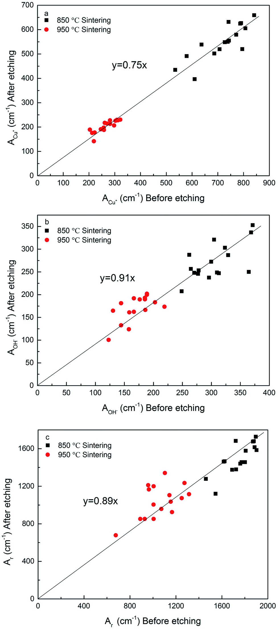 | ||
| Fig. 7 Correlations between surface areas of samples with and without the etching treatment for the LCS porous Cu samples sintered at two different temperatures: (a) ACu+ (b) AOH− and (c) Ar. | ||
Etching treatment also has a significant effect on the surface areas. There is a strong correlation between the surface areas before and after etching. The chemical etching resulted in reductions of 25% in the electroactive surface area measured by the diffusion of Cu+ (Fig. 7a) and 9% in the electroactive surface area measured by the diffusion of OH− (Fig. 7b), and 11% in the real surface area (Fig. 7c). That is because chemical etching significantly reduced the surface roughness of the LCS Cu samples, as evidenced in Fig. 3.
3.4 Effect of chemical reaction on electroactive surface area
Fig. 8 shows the relations between the volumetric electroactive surface area and real surface area for the LCS porous Cu samples manufactured with different Cu particles sizes and sintered at 850 °C and 950 °C, before and after chemical etching. A moderate level correlation exists between the electroactive and real surface areas. The electroactive surface area measured by the diffusion of OH− is approximately 16–18% of the real surface area, regardless of the manufacturing and treatment conditions. The ratio between the electroactive surface area measured by the diffusion of Cu+ and the real surface area depends on the manufacturing conditions. The ratio was approximately 40% for samples sintered at 850 °C, and reduced to 37% after etching. The ratio was 24% for samples sintered at 950 °C and further reduced to 19% after etching.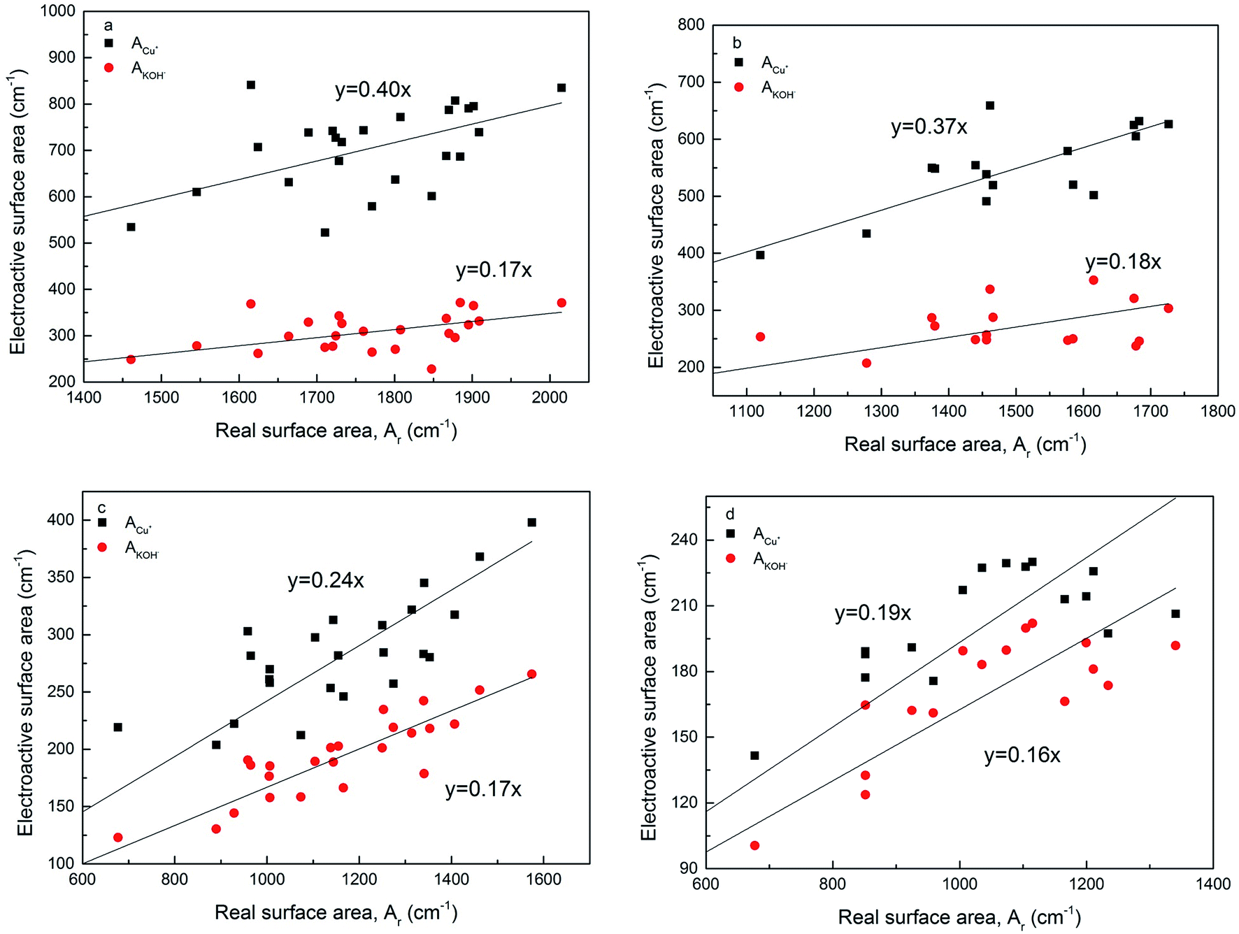 | ||
| Fig. 8 Correlations between electroactive surface area and real surface area for the LCS porous Cu samples sintered at (a) 850 °C, (b) 850 °C and etching, (c) 950 °C, and (d) 950 °C and etching. | ||
It was evident that the electroactive surface area depends on the electrochemical reaction being considered and the diffusion species involved in the reaction. The differences between AOH−, ACu+ and Ar can be explained by considering the thickness of the diffusion layer involved in the reaction. The Nernst diffusion layer thickness, δ, can be calculated by28
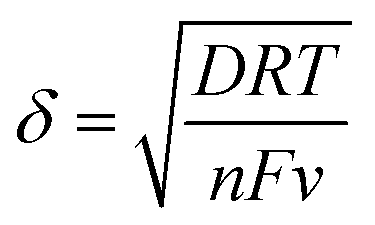 | (7) |
![[thin space (1/6-em)]](https://www.rsc.org/images/entities/char_2009.gif) 485 C mol−1) and v is the applied scan rate (0.01 V s−1). The diffusion layer thicknesses for OH− and Cu+, calculated by eqn (7), are about 50 μm and 1 μm, respectively.
485 C mol−1) and v is the applied scan rate (0.01 V s−1). The diffusion layer thicknesses for OH− and Cu+, calculated by eqn (7), are about 50 μm and 1 μm, respectively.
The real surface area is the maximum electroactive surface area that can contribute to any electrochemical reactions. Because no diffusion of reactive species is involved in the measurements of real surface area, the Nernst diffusion layer thickness can be regarded as zero. The surface features at all length scales contribute to the surface area. For reaction (1) controlled by the diffusion of Cu+, however, any features less than 1 μm in the LCS porous Cu, e.g., the very fine interstices/protrusions in the metal matrix formed by the sintered Cu particles, will be depleted with Cu+ ions rapidly due to limited supply characteristic of thin layer diffusion, as shown schematically in Fig. 9. The species are depleted because of a longer distance of diffusion from the electrolyte reservoir to the electrode surface at which the reaction takes place. Those interstices or protrusions with a size smaller than 1 μm can be ignored by the reaction,14–16 as they do not contribute fully to the current density and thus cannot be detected. The electroactive surface area is effectively the contour or boundary of the diffusion layer within the solid Cu. Similarly, for reaction (2) controlled by the diffusion of OH−, any features less than 50 μm in the LCS porous Cu will not contribute fully to the current density and thus cannot be detected as part of the electroactive surface area. In this case, the electroactive surface area is effectively the contour or boundary of the diffusion layer within the electrolyte (Fig. 9).
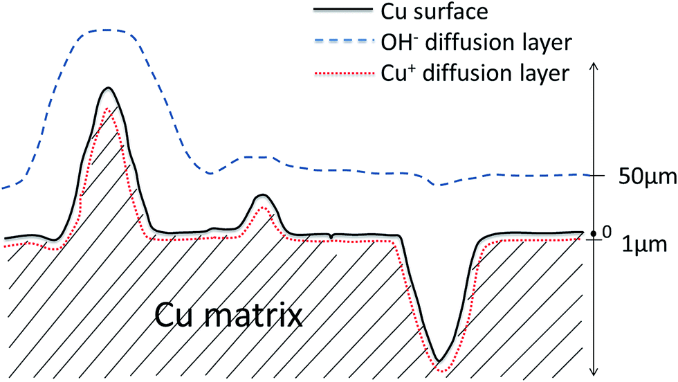 | ||
| Fig. 9 Schematic of diffusion layers of OH− and Cu+ at the interface between Cu matrix and electrolyte. | ||
In short, the double capacitance method and the cyclic voltammetry method based on diffusion controlled reactions can measure the electroactive surface areas at different length scales. The double capacitance method can detect all features of the surface. The CV method based on the diffusion of Cu+ ions can only detect surface features bigger than 1 μm, while the CV method based on the diffusion of OH− ions can only detect surface features bigger than 50 μm. As a consequence, the real surface area is greater than the electroactive surface area for Cu+ diffusion, which in turn is greater than the electroactive surface area for OH− diffusion.
Fig. 8 also shows that while the ratio between AOH− and Ar did not change with process conditions, the ratio between ACu+ and Ar changes with sintering temperature and chemical etching. The different behaviour in ACu+ is likely because reaction (1) is not solely controlled by Cu+ diffusion. In the region of the solid electrode near the interface with the electrolyte, there is sufficient supply of OH− ions and the reaction is controlled by the Cu+ diffusion in the solid phase. In the region farther away from the interface with the electrolyte, i.e., in the interior of the cell wall, the supply of OH− ions is also limited by the diffusion of the OH− ions in the electrolyte. The reaction becomes both Cu+ and OH− diffusion controlled.
4. Conclusions
(1) Two electrochemical reactions are involved in the cyclic voltammetry of Cu. The electroactive surface area of the LCS porous Cu depends on the reaction being considered and the diffusion layer thickness associated with the reaction.(2) A thicker diffusion layer results in a lower electroactive surface area. The electroactive surface areas based on the diffusion of Cu+ in the solid phase and OH− in the electrolyte, with the diffusion layer thicknesses of 1 μm and 50 μm, are approximately 16–18% and 19–40% of the real surface area, respectively. The former is largely independent of the manufacturing conditions, while the latter depends on the sintering temperature and etching treatment.
(3) The particle size of the Cu powder used to manufacture the LCS porous Cu had a modest effect on the electroactive and real surface areas, with the medium particle sizes, 20–45 μm or 45–75 μm, showing the highest surface areas.
(4) Increasing sintering temperature from 850 °C to 950 °C reduced the electroactive and real surface areas by 31–61%. Chemical etching reduced the electroactive and real surface areas by 9–25%.
References
- M. F. Ashby, T. Evans, N. A. Fleck, J. Hutchinson, H. Wadley and L. Gibson, Metal Foams: A Design Guide: A Design Guide, Elsevier, 2000 Search PubMed.
- X. Huang, J. Tu, X. Xia, X. Wang and J. Xiang, Electrochem. Commun., 2008, 10, 1288–1290 CrossRef CAS.
- H. Wang, Q. Pan, X. Wang, G. Yin and J. Zhao, J. Appl. Electrochem., 2009, 39, 1597–1602 CrossRef CAS.
- R. Shivkumar, G. P. Kalaignan and T. Vasudevan, J. Power Sources, 1998, 75, 90–100 CrossRef CAS.
- K. Naito, T. Matsunami, K. Okuno, M. Matsuoka and C. Iwakura, J. Appl. Electrochem., 1993, 23, 1051–1055 CrossRef CAS.
- M. C. Tucker, G. Y. Lau, C. P. Jacobson, L. C. DeJonghe and S. J. Visco, J. Power Sources, 2007, 171, 477–482 CrossRef CAS.
- S. Molin, B. Kusz, M. Gazda and P. Jasinski, J. Power Sources, 2008, 181, 31–37 CrossRef CAS.
- V. Ganesh, V. Lakshminarayanan and S. Pitchumani, Electrochem. Solid-State Lett., 2005, 8, A308–A312 CrossRef CAS.
- F. Bidault, D. Brett, P. Middleton, N. Abson and N. Brandon, Int. J. Hydrogen Energy, 2009, 34, 6799–6808 CrossRef CAS.
- A. Đukić, V. Alar, M. Firak and S. Jakovljević, J. Alloys Compd., 2013, 573, 128–132 CrossRef.
- G. W. Nyce, J. R. Hayes, A. V. Hamza and J. H. Satcher, Chem. Mater., 2007, 19, 344–346 CrossRef CAS.
- K. K. Diao, Z. Xiao and Y. Y. Zhao, Mater. Chem. Phys., 2015, 162, 571–579 CrossRef CAS.
- P. Delahay, New Instrumental Methods, in Electrochemistry: Theory, Instrumentation, and Applications to Analytical and Physical Chemistry. With a Chapter on High-frequency Methods, Interscience Publishers, 1954 Search PubMed.
- E. O. Barnes, X. Chen, P. Li and R. G. Compton, J. Electroanal. Chem., 2014, 720, 92–100 CrossRef.
- T. J. Davies and R. G. Compton, J. Electroanal. Chem., 2005, 585, 63–82 CrossRef CAS.
- T. J. Davies, S. Ward-Jones, C. E. Banks, J. del Campo, R. Mas, F. X. Munoz and R. G. Compton, J. Electroanal. Chem., 2005, 585, 51–62 CrossRef CAS.
- R. E. Smith, T. J. Davies, N. D. B. Baynes and R. J. Nichols, J. Electroanal. Chem., 2015, 747, 29–38 CrossRef CAS.
- M. Grdeń, M. Alsabet and G. Jerkiewicz, ACS Appl. Mater. Interfaces, 2012, 4, 3012–3021 Search PubMed.
- Y. H. Tan, J. A. Davis, K. Fujikawa, N. V. Ganesh, A. V. Demchenko and K. J. Stine, J. Mater. Chem., 2012, 22, 6733–6745 RSC.
- S. Rausch and H. Wendt, J. Electrochem. Soc., 1996, 143, 2852–2862 CrossRef CAS.
- R. Campbell, M. G. Bakker, C. Treiner and J. Chevalet, J. Porous Mater., 2004, 11, 63–69 CrossRef CAS.
- Y. Y. Zhao, T. Fung, L. P. Zhang and F. L. Zhang, Scr. Mater., 2005, 52, 295–298 CrossRef CAS.
- Y. Y. Zhao and L. P. Zhang, Proc. Inst. Mech. Eng., Part B, 2008, 222, 267–271 CrossRef.
- N. Hampson, J. Lee and K. Macdonald, J. Electroanal. Chem. Interfacial Electrochem., 1972, 34, 91–99 CAS.
- J. Ambrose, R. Barradas and D. Shoesmith, J. Electroanal. Chem. Interfacial Electrochem., 1973, 47, 47–64 CrossRef CAS.
- A. Lewandowski, P. Jakobczyk and M. Galinski, Electrochim. Acta, 2012, 86, 225–231 CrossRef CAS.
- A. Łukomska and J. Sobkowski, J. Electroanal. Chem., 2004, 567, 95–102 CrossRef.
- C. Amatore, Physical Electrochemistry: Principles, Methods and Applications, 1995, 4, 131–208 Search PubMed.
Footnote |
| † Electronic supplementary information (ESI) available. See DOI: 10.1039/c7ra04204c |
| This journal is © The Royal Society of Chemistry 2017 |