
Lead-free tin chalcogenide thermoelectric materials
Min
Zhou
*a,
G. Jeffrey
Snyder
 bc,
Laifeng
Li
a and
Li-Dong
Zhao
*d
bc,
Laifeng
Li
a and
Li-Dong
Zhao
*d
aKey Laboratory of Cryogenics, Technical Institute of Physics and Chemistry, Chinese Academy of Sciences, Beijing 100190, China. E-mail: mzhou@mail.ipc.ac.cn
bDepartment of Materials Science and Engineering, Northwestern University, Evanston, Illinois 60208, USA
cITMO University, St Petersburg, Russia
dSchool of Materials Science and Engineering, Beihang University, Beijing 100191, China. E-mail: zhaolidong@buaa.edu.cn
First published on 10th September 2016
Abstract
Thermoelectric materials can be used to directly and reversibly convert waste heat into electrical power and have attracted significant attention. Lead-free tin chalcogenide (SnTe, SnSe, SnS) thermoelectric materials are regarded as promising thermoelectric materials due to the great progress in the thermoelectric research field during the past several years. Analogous to PbTe, SnTe has a simple high symmetry NaCl-type cubic structure and a complex band structure, leading to its capability of achieving high thermoelectric performance by band structure and microstructure engineering. SnSe/SnS are simple compounds but exhibit an intrinsically ultralow thermal conductivity, suggesting that a high thermoelectric performance can be realized also in simple layered, anisotropic and anharmonic systems, without nanostructuring. This short perspective summarizes some current strategies that could enhance the thermoelectric performance of bulk lead-free tin chalcogenides, such as band structure engineering, nanostructuring, and synergistically improved approaches. Future possible strategies for further enhancing the thermoelectric performance of tin chalcogenides are also considered at the end of this perspective.
 Min Zhou | Min Zhou is an associate professor at the Technical Institute of Physics and Chemistry, Chinese Academy of Sciences, China. She completed her postdoctoral research at Tsinghua University in 2007. She received her PhD degree in materials science and engineering from the Shanghai Institute of Ceramics, Chinese Academy of Sciences, China in 2005. Her main research interests focus on thermoelectric materials and their application in the field of energy conversion. |
 G. Jeffrey Snyder | G. Jeffrey Snyder is a Professor of Materials Science and Engineering at Northwestern University in Evanston Illinois. His interests are focused on materials physics and chemistry for thermoelectric engineering, such as band engineering, the design of complex Zintl compounds and the use of nanostructured composites. His interdisciplinary approach stems from studies of Solid State Chemistry at Cornell University and the Max Planck Institute for Solid State Research, Applied Physics at Stanford University and thermoelectric materials & device engineering at NASA/Jet Propulsion Laboratory and California Institute of Technology (Caltech). |
 Laifeng Li | Laifeng Li is a Professor at the Technical Institute of Physics and Chemistry, Chinese Academy of Sciences, China. He received his PhD degree in Condensed Matter Physics from the Institute of Physics, CAS in 1996. He completed a postdoctoral research University of Michigan in 1998. His research interests include cryogenic materials and superconductors. |
 Li-Dong Zhao | Li-Dong Zhao was born in Harbin, China in 1979. He is a Professor of Materials Science and Engineering at Beihang University, China. He received his B.E. and M.E. degrees in Materials Science from the Liaoning Technical University, and his Ph.D. degree in Materials Science from the University of Science and Technology Beijing, China in 2009. He was a postdoctoral research fellow in the LEMHE-ICMMO (CNRS-UMR 8182) at the University of Paris-Sud from 2009 to 2011, and a postdoctoral research fellow in the Department of Chemistry at the Northwestern University from 2011 to 2014. He is a recipient of “the Thousand Talents Plan” 2015. His research interests include thermoelectric materials, superconductors and thermal barrier coatings. |
1. Introduction
Thermoelectric materials have drawn vast attention for centuries because thermoelectric effects can directly and reversibly convert heat into electrical power, thus providing an alternative for power generation and refrigeration. The conversion efficiency of thermoelectric technology is governed by the thermoelectric figure of merit (zT), defined as zT = α2σT/(κL + κe), where α is the Seebeck coefficient, σ is the electrical conductivity, T is the absolute temperature, and κe and κL are the electron thermal conductivity and lattice thermal conductivity (total thermal conductivity, κ = κe + κL), respectively. To maximize the thermoelectric figure of merit (zT) of a material, a large Seebeck coefficient, a high electrical conductivity, and a low thermal conductivity are needed. However, these parameters are determined by the inter-dependent relationships of the electronic structure and scattering of charge carriers (electrons or holes), and thus are not independently controllable. For metals or degenerate semiconductors (parabolic band, energy-independent scattering approximation1), the Seebeck coefficient is proportional to the temperature and effective mass (m*), and inversely proportional to the charge carrier concentration (n), as seen in eqn (1). Thus, a large Seebeck coefficient translates to a large effective mass which is equivalent to a large density-of-states (DOS) or flat bands at the Fermi level. High electrical conductivity requires a large mobility (μ) and a large carrier (electrons or holes) concentration (n) through eqn (2). Therefore, high zT requires a combination of a large Seebeck coefficient (α) with a high electrical conductivity (σ). This is typically only achieved in heavily doped semiconductors combining high electron density-of-states (high effective masses) with high carrier concentrations, and high mobility2 as seen in eqn (1) and (2).For metals or degenerate semiconductors (parabolic band, energy-independent scattering approximation1) the Seebeck coefficient is given by:
 | (1) |
The electrical conductivity (σ) is related to n through the carrier mobility μ:
| σ = neμ | (2) |
| κ = κe + κL | (3) |
| κe = LσT = neμLT | (4) |
Good thermoelectric materials are therefore crystalline materials of “phonon glass–electron crystal”.2 The electron-crystal requirement stems from the fact that crystalline semiconductors have been the best at meeting the compromises required from the electronic properties (Seebeck coefficient and electrical conductivity). The phonon-glass requirement stems from the need for as low a lattice thermal conductivity as possible. Over the past decades, research on bulk thermoelectric materials has made great progress by diverse strategies (for example, band structure engineering, phonon engineering and seeking new promising thermoelectric systems)4,5,13–20 and the figure of merit (zT) reached even higher than 2.
Thermoelectric materials that are used in mid-temperature (500–1000 K) power generation are particularly attractive because most of the waste heat in industry and automobile exhaust is within this range.21,22 To date, the leading materials include lead chalcogenides,4,13,23–27 filled skutterudites,28–32 half-Heusler compounds,33–36etc. In recent years, tin chalcogenides have attracted increasing interest due to their greatly enhanced thermoelectric performance by band engineering and/or naonostructure,15,18,37–43 and lattice anharmonicity.15,44
Skutterudites are a highly promising and deeply researched class of compounds. Since the void-filling atoms in skutterudites can act as electron donors or acceptors, partially filling the void space of skutterudites could lead to an optimum electron concentration. At the same time, these atoms can also act as strong phonon-scattering centers to greatly reduce the lattice thermal conductivity. Recently, numerous investigations have been carried out on skutterudites with respect to the in-depth study of the physical process theory and the discovery of novel filled compounds. The thermoelectric performance of these materials has been greatly increased by both doping/filling45–48 and nanostructure/nanocomposites strategies.31,49–57 On the basis of the “rattling” concept, the thermal conductivity was significantly reduced by single-, double-, triple-, and multiple-filling of elements into voids of the skutterudite structure, resulting in an improvement of zT values.58–60 A high zT of 1.8 was reported in quadruple filled n-type skutterudites (Sr, Ba, Yb, In)yCo4Sb12 at 823 K. In porous (Ba,In) double-filled skutterudite materials a maximum zT of 1.36 was obtained, in which the Seebeck coefficient was increased due to the electron filtering effect induced by nanostructures on the surfaces of pores, and the lattice thermal conductivity was dramatically suppressed due to the enhanced pore-edge boundary scattering of long-wavelength phonons.51 Besides, the compaction technique, hot press together with high-pressure torsion (HPT), is a new method for reducing the thermal conductivity (up to 40%) of skutterudites due to the additionally introduced defects.61,62 The zT value could be further enhanced to 1.9 at 835 K for Sr0.09Ba0.11Yb0.05Co4Sb12 after severe plastic deformation via high-pressure torsion.62 The thermoelectric properties of semiconductors are intimately related to their electronic band structure, which can be engineered via chemical doping.63,64 A high zT value of 1.3 was reported in YbxCo4Sb12 at 850 K due mainly to the band convergence of the light conduction band with the heavy conduction.65
Another class of potential thermoelectric compounds is half-Heusler compounds. The most attractive feature of half-Heusler alloys as promising thermoelectric materials is their large Seebeck coefficient (approximately 100 μV K−1 at room temperature) and high electrical conductivities (1000–10![[thin space (1/6-em)]](https://www.rsc.org/images/entities/char_2009.gif) 000 S cm−1).34,66 However, on account of their relatively high thermal conductivity, the zT values of half-Heusler compounds are still much lower than those of the state-of-the-art thermoelectric materials. The thermoelectric properties in isoelectronic-alloyed half-Heusler compounds were increased through induced mass fluctuations and strain field effects.35,66–68 In recent year, half-Heusler compounds, such as MNiSn, MCoSb (M = Ti, Zr, Hf) and FeRSb (R = V, Nb), have gained popularity. Much work has been done on optimization of the electrical transport properties by tuning the carrier concentration67–69 and suppressing the lattice thermal conductivity by alloying or nanostructuring.35,66–68,70–73 A high zT of about 1.0 was reported for both n-type and p-type HH compounds.36,67,69,70 Further improvement of zT was realized in p-type FeNb1−xHfxSb heavy-band half-Heusler alloys due mainly to the enhanced point-defect and electron–phonon scattering by the high content of the heavier Hf dopant. A high zT of 1.5 was reported at 1200 K.74
000 S cm−1).34,66 However, on account of their relatively high thermal conductivity, the zT values of half-Heusler compounds are still much lower than those of the state-of-the-art thermoelectric materials. The thermoelectric properties in isoelectronic-alloyed half-Heusler compounds were increased through induced mass fluctuations and strain field effects.35,66–68 In recent year, half-Heusler compounds, such as MNiSn, MCoSb (M = Ti, Zr, Hf) and FeRSb (R = V, Nb), have gained popularity. Much work has been done on optimization of the electrical transport properties by tuning the carrier concentration67–69 and suppressing the lattice thermal conductivity by alloying or nanostructuring.35,66–68,70–73 A high zT of about 1.0 was reported for both n-type and p-type HH compounds.36,67,69,70 Further improvement of zT was realized in p-type FeNb1−xHfxSb heavy-band half-Heusler alloys due mainly to the enhanced point-defect and electron–phonon scattering by the high content of the heavier Hf dopant. A high zT of 1.5 was reported at 1200 K.74
Lead chalcogenides and their solid solutions are among the most efficient thermoelectric materials in the mid-temperature region. PbTe, in particular, has a long history as a thermoelectric material and has been used in practical applications since the 1950s.75,76 Recently, the thermoelectric figure of merit (zT) of lead chalcogenides was continuously increased by synergistically using the concepts of band engineering (resonant levels,23,24,77 band convergence,13,26,78 bands alignment,5,79,80etc.) and microstructure manipulation on all scaled hierarchical architectures.4,5,80–82 A high zT value of 2.2 was reported for nanostructured AgPbmSbTe2+m at 800 K in 2008.4 In the past several years, the thermoelectric performance of lead chalcogenides was enhanced and a higher zT of 2.5 (923 K) was even reached for heavily alloyed PbTe–x%SrTe in 2016, in which significant band convergence boosted the power factors through non-equilibrium processing and endotaxial SrTe nanostructures greatly decreased the lattice thermal conductivity.83 However, the environmental concern regarding Pb in lead chalcogenides can hinder their development and large-scale application.
In 2014, an outstandingly high zT value of 2.6 at 923 K was reported in SnSe crystals,15 which have attracted a great deal of interest in research on lead-free tin chalcogenides. In the past several years, the thermoelectric performance of tin chalcogenides (SnTe, SnSe, SnS) was greatly increased by band engineering and/or naonostructures.15,18,39–43,84,85 A high zT value of even 1.35–1.4 was reported in Hg-doped SnTe and In/Cd-codoped SnTe with CdS nanostructures.60 These research studies suggest that tin chalcogenides are attracting increasing attention as robust candidates of lead chalcogenides for thermoelectric power generation.15,85–87 It is worth noting that the local ferroelectric ordering was directly observed by piezo-response force microscopy (PFM) in SnTe above room temperature.88 Then, Chang et al. discovered stable in-plane ferroelectricity in atomic-thick SnTe thin films, even down to a 1 unit cell (UC) limit.89 These findings make SnTe an important member of the new family of multi-functional materials, namely ferroelectric–thermoelectrics. Table 1 lists zT peaks and the corresponding temperature for some leading materials in the mid-temperature range (500–1000 K).
Our goal herein is to highlight the progress of research on promising tin chalcogenides (SnTe, SnSe and SnS) in recent years. This paper is not an exhaustive review; although lead chalcogenides are a significant part of thermoelectric research, they are beyond the scope of the current review. In this perspective, recent advances in the field of tin chalcogenide (SnTe, SnSe and SnS) bulk alloys are summarized, e.g., band structure engineering strategies (resonant impurity doping and band convergence) lead to profound changes in the electrical properties. And nanostructuring/lattice anharmonicity strategies cause low lattice thermal conductivity. Future possible strategies for further enhancing the thermoelectric performance of tin chalcogenides are also considered in this perspective.
2. SnTe and its solid solutions
Among tin chalcogenides (SnTe, SnSe and SnS), only SnTe has a rock salt crystal structure and shows isotropic thermoelectric properties. The stoichiometric SnTe is inherently riddled with Sn vacancies, which normally results in a heavily doped (1020–1021 cm−3) p-type semiconductor.92–96 Such a high carrier concentration results in very high electrical conductivity (∼7000 S cm−1 at room temperature), but an extremely low Seebeck coefficient (corresponding to the minimum value of the Seebeck coefficient in the Pisarenko plot, as shown in Fig. 1b) and a high electrical thermal conductivity.92 Therefore, SnTe did not receive extensive attention due to its poor thermoelectric performance (a mediocre zT of about 0.5 at 900 K) in the past decades.92,96 Besides, a very small band gap (0.18 eV at room temperature) leads to a significant bipolar transport behavior, and a large energy offset between the light valence band (L) and the heavy valence band (Σ) (ΔE, 0.3–0.4 eV at room temperature)92–95 hinders the contribution of the heavier holes to the Seebeck coefficients (as shown in Fig. 1a). It is therefore essential to modify the carrier concentration to more optimal levels with the aim of further enhancing the thermoelectric performance. Besides, recent studies unambiguously show that SnTe has a strong potential of being a good thermoelectric material through band structure engineering (band convergence, resonant doping, etc.) and/or nanostructure engineering.85–87,97–100 | ||
| Fig. 1 (a) A schematic diagram of the near edge band structure in SnTe and PbTe. Both feature two valence bands separated by an energy difference (ΔE) at room temperature. (b) The Seebeck coefficient as a function of Hall carrier concentration (Pisarenko relation) at 300 K. The SnTe compound has a smaller band gap (Eg, 0.18 eV) and larger energy offsets between the light valence band (VBL) and the heavy valence band (VBΣ) (ΔE, 0.3–0.4 eV) with respect to PbTe (Eg, 0.30 eV and ΔE, close to 0.1 eV at 300 K, respectively). Compared with the single band, the heavy valence band causes a Pisarenko line upturn. On increasing the Hall carrier concentration, the carrier transport of SnTe undergoes three regions, region I (light valence band), region II (light valence band + partial heavy valence band), and region III (light valence band + heavy valence band).99,101,102 (Reproduced with permission from J. Am. Chem. Soc., 2016, 138, 2366. Copyright 2016 American Chemical Society). | ||
2.1 Carrier concentration optimization
As mentioned above, SnTe is normally a highly degenerate p-type semiconductor with a high carrier concentration (1020–1021 cm−3) ascribed to the intrinsic Sn deficiency, making it a poor thermoelectric material.96,103 To improve thermoelectric performance, it is necessary to either lower the carrier concentration to take advantage of the light L band or modify the band structures for better band convergence. It is found that bismuth, antimony, and iodine are effective donors to reduce the hole concentration in SnTe.93,95,99 On the other hand, Sn self-compensation is also an effective way of neutralizing the overly high hole concentration of SnTe.87 Zhou et al. investigated the effects of both donor- and acceptor-doping on the Hall carrier concentration and thermoelectric properties in SnTe.95 It is found that donor-doping (iodine) decreased the Hall carrier concentration, which enhanced the Seebeck coefficient and zT values utilizing the high mobility of the light band. Strikingly in contrast to the normal Pisarenko relationship based on the single parabolic band (SPB) model, acceptor-doping (extra Te or Gd), which increases the Hall carrier concentration, also increases the Seebeck coefficient, due to the dominant contribution from the heavy valence band. A two-band model (a Kane band for the light and a parabolic band for the heavy valence band) has been used to fit the experimental data of both the Seebeck coefficient and zT values. It is found that only a single maximum in zT was seen in most thermoelectric materials at higher temperatures although the Seebeck coefficient reached peak values at a carrier concentration of nH ≈ 4–6 × 1020 cm−3 (as shown in Fig. 2). Experimentally, a maximum zT value of 0.6 (700 K) was obtained at nH ≈ 4 × 1019 cm−3 due to the solid solubility limit of iodine in SnTe. Therefore, optimizing the SnTe carrier concentration towards the light band without obviously altering the host band structure is a valid approach to improve the thermoelectric properties of the SnTe compound. | ||
| Fig. 2 (a) Seebeck coefficient and (b) zT as a function of Hall carrier concentration for donor-doped and acceptor-doped SnTe compounds. The black dashed vertical line in (a) and (b) corresponds to the undoped SnTe (nH ≈ 1.1 × 1020 cm−3 at room temperature). The black open squares are Rogers’ reported results.95 The black solid squares, the dark yellow circles and the red diamonds are Zhou's reported results at 300 K, 600 K and 773 K, respectively.95 The solid curves are the fitted zT values with the two-band model, and the dashed lines are the uncertainty values. (Reproduced with permission from Phys. Chem. Chem. Phys., 2014, 16, 20741. Copyright 2014 Royal Society of Chemistry). | ||
2.2 Band structure engineering
The complex band structure of SnTe leads to some strategies based on band structure engineering. Further enhancements of zT values were recently reported through DOS distortion (In doping)86,97 around room temperature and through valence band convergence (Cd, Hg, Mg, Ca and Mn alloying) individually37,43,85,87,98,100,104,105 above room temperature or simultaneously in a broad temperature range through In/Cd co-doping.97Fig. 3a shows a schematic representation of the density of electron states (DOS) of multiple valence bands and of the resonant states added to the host band. Compared with the host SnTe compound, a great enhancement of Seebeck coefficient is observed in In-doped SnTe (a resonant dopant in SnTe) at a given doping concentration where additional energy states were added to the host band.86,97 The calculation of the band structure of M-doped SnTe (M = Ga, In, Tl) confirmed that only In-doping introduces an obvious resonant state near the Fermi level. The resonant state was demonstrated to be from the anti-bonding of In-s and Te-p orbitals.106
 | ||
| Fig. 3 (a) Schematic representation of the density of states of multiple bands and resonant impurity.107 Both the resonant states and multiple bands increase the density of states and the Seebeck coefficient. (b) The enhancement of Seebeck coefficient at a similar Hall carrier concentration in SnTe-based compounds due to resonant doping (In) at room temperature. Solid symbols correspond to the data of In-doped SnTe with different In contents. Open symbols correspond to the data without resonant dopants. The solid curve represents the results of the two-band model. (Reproduced with permission from Adv. Mater., 2012, 24, 6125. Copyright 2012 John Wiley and Sons Inc.). | ||
In contrast to In-doped SnTe, the Seebeck coefficient of SnTe-based compounds without resonant dopants increases at higher carrier concentration (1020–1021 cm−3) (as shown in Fig. 3b), which can be attributed to the heavy valence band in SnTe.93,95 A high Seebeck coefficient value of about 80 μV K−1 was obtained for In-doped SnTe at room temperature,86,97 which is higher than that of heavily doped SnTe.93 However, the enhancement of the Seebeck coefficient diminishes with increasing temperature.86,97 This is similar to the case of the Tl-doped PbTe system, which only exhibits Seebeck coefficient enhancements at room temperature and below, but the effect weakens significantly above 500 K.24 The synergistic combination of DOS distortion and nanostructure leads to a maximum zT of 1.1 at 873 K in In-doped SnTe.86
Based on the enhanced Seebeck coefficient in In-doped SnTe, to achieve high thermoelectric performance over a broad temperature range, a careful control of the doping level and the position of the resonant levels is needed. This leads to studies of co-doped SnTe where the amounts of resonant impurity (In) and extrinsic dopants (iodine, Ag, extra Te) are adjusted independently. Fig. 4 shows the composition dependences of the Hall carrier concentration and Seebeck coefficient in co-doped SnTe with In and additional impurities (iodine, Ag, extra Te). Analogous to Tl-doped PbTe with additional Na impurity or excess Pb,108 the Hall carrier concentration (nH) is stabilized over a broad range of additional impurities, which is called the stabilization region. From a simple chemistry point of view, in the presence of additional Te/Ag acceptors, the valence of some In atoms changes from In1+ to In3+ compensating for the free hole generated by extra Te/Ag. By contrast, In3+ changes to In+ with additional iodine donors in the SnTe compound. That is, in the stabilization region the In impurity suppressed extrinsic doping and stabilized (pinned) the Fermi level.109 Similar to Tl resonant states in PbTe,108 the presence of two states (In+ and In3+) per In atom provides an explanation for the amphoteric character of the given In impurity. Upon substituting additional co-dopants (I donors or extra Te/Ag acceptors) beyond the stabilization region, the Hall carrier concentration changed in proportion to the additional impurity content (NI, NTe/NAg) (called the doping region), indicating that the Fermi level is no longer pinned at the resonant level.110
 | ||
| Fig. 4 (a) Hall carrier concentration and (b) Seebeck coefficient of co-doped In0.01Sn0.99Te1−yIy (left side of the abscissa) and In0.01AgzSn0.99−zTe/In0.01Sn0.99Te1+x (right side of the abscissa) compounds at 300 K. The solid squares and open squares are Zhou's and Bushmarina's reported results, respectively.110 | ||
As shown in Fig. 4b, higher Seebeck coefficients are found within the stabilization region, whereas it decreases when the carrier density is either below or above it. This is a result of a weakened influence from resonant levels as the Fermi level moves away. Also note that Seebeck coefficients in samples with resonant levels are always higher than those without them given the same carrier density, which is due to the increased density of states (DOS) in SnTe with In impurities.110
As discussed above, the introduction of In in SnTe could create resonant levels inside the valence band, which enhances the Seebeck coefficient around room temperature.24,77 A similarly enhanced Seebeck coefficient at a given carrier concentration has also been found in Sn1−xMxTe (M = Hg, Cd, Mn, Ca, Mg) due to a band convergence effect37,43,85,87,100,104 (as shown in Fig. 5). Fig. 5(a) shows a schematic energy diagram of the near edge band structure in SnTe and Sn1−xMxTe (M = Hg, Cd, Mn, Ca, Mg). Compared with SnTe, M-doping (M = Hg, Cd, Mn, Ca, Mg) opens the band gap and diminishes the band offset between the light valence band and the heavy valence band (band convergence). The band gap enlargement also reduces the number of minority carriers at elevated temperature and suppresses the bipolar diffusion. The band offset reduction also results in the more efficient contribution of the heavy valence band to transport properties, enhancing the Seebeck coefficient, especially at high temperature. Tan et al. carried out density functional theory calculations of the electronic structures and confirmed the above modification of the band gap by Cd/Hg alloying.85,87 Similar band modifications have been found in Cd- and Mg-doped PbTe26,78 and PbSe.27 From Fig. 5(b), it is clear that M-doped SnTe (M = Hg, Cd, Mn, Ca, Mg) compounds have much higher Seebeck coefficient than those without band convergence for a similar hole concentration at room temperature. At high temperature, the increased valence band degeneracy also leads to an enhancement of the Seebeck coefficient because both valence bands are contributing efficiently to the transport properties.
 | ||
| Fig. 5 (a) Schematic energy diagram of the near edge band structure in SnTe and Sn1−xMxTe (M = Hg, Cd, Mn, Ca, Mg). Eg is the bandgap, and ΔE is the band offset between the light valence band (VBL) and the heavy valence band (VBΣ). The relative positions of the conduction band (CB), the light valence band and the heavy valence band are shown for the undoped SnTe and doped Sn1−xMxTe (M = Hg, Cd, Mn, Ca, Mg). (b) Seebeck coefficient as a function of Hall carrier concentration for Sn1−xMxTe (M = Hg, Cd, Mn, Ca, Mg). The black squares, the red circles, the blue triangles and the magenta diamonds represent the results of Hg-doepd, Cd-doped, Ca-doped and Mg-doped SnTe. The purple left-triangles, the green right-triangles and the red stars represent the results of Mn-doped SnTe. The red open circles are the results of the Cd/In-codoped SnTe. The open diamonds and down-triangles are doped SnTe without band convergence or resonant doping. Solid curves are the results of the two-band model. | ||
It is worth noting that Hg-doped SnTe has a lower lattice thermal conductivity compared to the Cd-doped SnTe.85 This is mainly attributed to the larger atomic radius and mass difference between Hg and Sn, which could cause stronger point defect scattering. A high maximum zT of 1.35 (900 K) and an average zTave (300–900 K) of 0.84 were reported for Hg-doped SnTe material.85
The coexistence of resonant levels induced by In doping and band convergence enabled by Cd doping in SnTe produces a significant enhancement of the Seebeck coefficient and zT values over a broad temperature range.97 As shown in Fig. 6, the Seebeck coefficient of the In/Cd co-doped SnTe is significantly higher than that of the pristine SnTe at room temperature, which is very similar to In-doped SnTe.86,97 Moreover, these In/Cd co-doped samples have large Seebeck coefficients (∼200 μV K−1) at 923 K that are very close to those of Cd-doped ones (Fig. 6a).97 These indicate that resonant levels introduced by the In dopant and band convergence caused by the Cd dopant may synergistically and harmoniously coexist in In and Cd codoped SnTe. First-principles density functional theory (DFT) calculations confirmed the coexistence of resonant levels and valence band convergence in In and Cd co-doped SnTe. The band offset (ΔE) between the light valence band and the heavy valence band decreases markedly to only 0.12 eV upon Cd-doping (as shown in the inset in Fig. 6a). In and Cd co-doping yields an even lower ΔE of 0.04 eV.97 It can therefore be concluded that band convergence still exists and plays a significant role in In/Cd co-doped SnTe. However, it is a challenge to differentiate the two effects experimentally.
 | ||
| Fig. 6 Temperature dependence of (a) the Seebeck coefficient and (b) zT values for the pristine SnTe, In-doped, Cd-doped and In/Cd-codoped SnTe. The inset in (a) is the band offset (ΔE) between the light valence band (VBL) and the heavy valence band (VBΣ) of the pristine SnTe, In-doped, Cd-doped and In/Cd-codoped SnTe at room temperature. The inset in (b) shows the maximum zT values (zTmax) and the average zT values (zTave) of the pristine SnTe, In-doped, Cd-doped and In/Cd-codoped SnTe. | ||
Combining the approaches of resonant levels and band convergence to modify the electronic structure of SnTe individually, one can readily improve both zTmax and zTave due to the broad enhancement of Seebeck coefficients. As shown in Fig. 6b, In-doping significantly increases the zT of SnTe in the low temperature range, while the zT values of Cd-doped SnTe increase rapidly with increasing temperature. As a result, a maximum zTmax value of 1.1 (923 K) and an average zTave of nearly 0.5 between 300 and 923 K were reported for In/Cd codoped SnTe.97
2.3 Synergistically optimizing the electrical and thermal transport properties
The band engineering and carrier concentration optimization were reviewed to enhance the thermoelectric performance of SnTe, especially by modifying the electrical transport properties. Synergistic modification of the electrical and thermal transport properties of SnTe can greatly increase zT values. Fig. 7 shows the maximum zT values of nanostructured SnTe-based materials at 823 K,99 suggesting greatly enhanced zT values with endotaxial nanostructures (SrTe, CdS, etc.).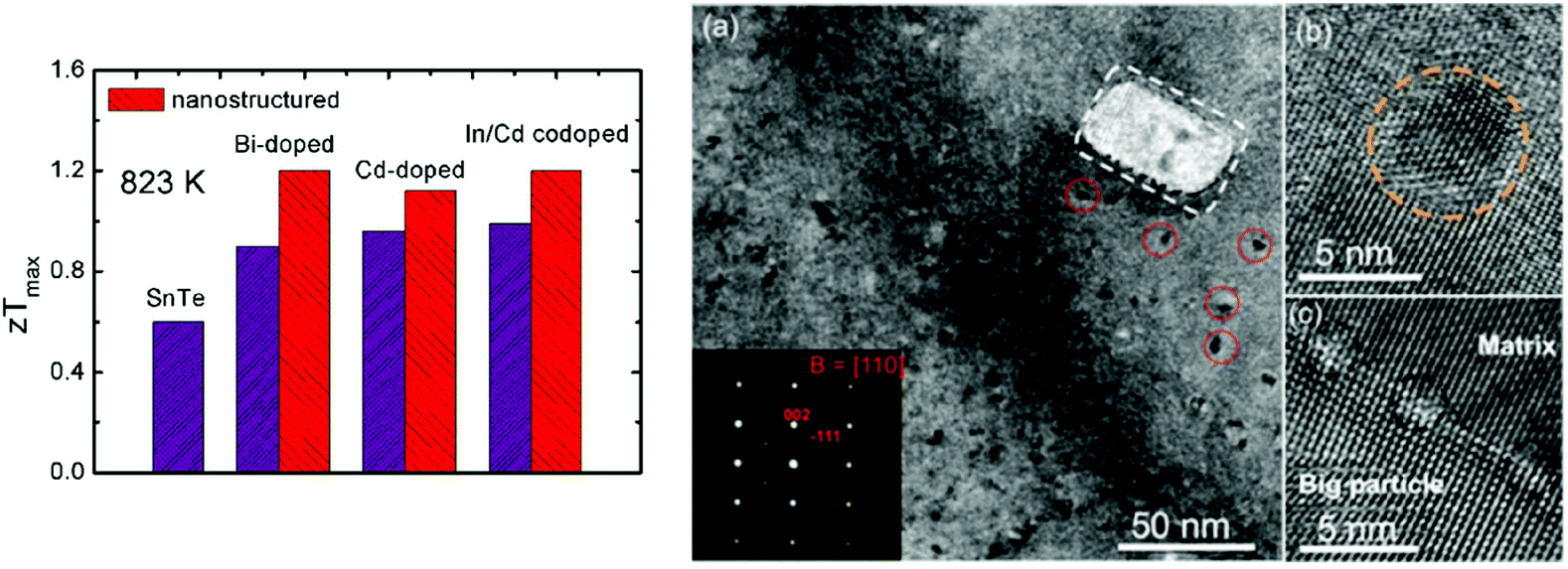 | ||
| Fig. 7 A comparison of the maximum zT values for the SnTe-based compounds with and without nanostructures. The right photograph shows an electron microscopy image of Sn0.97In0.015Cd0.015Te–3%CdS with CdS nanoscale precipitates.97 (Reproduced with permission from J. Am. Chem. Soc., 2015, 137, 5100. Copyright 2015 American Chemical Society). | ||
The electrical transport properties of SnTe were optimized by tuning the carrier concentration to about 1019 cm−3 by using donor-doping (I, Bi, Sb, etc.). The second phases (SrTe) were introduced into Bi-doped SnTe, forming effective strained endotaxial nanostructures to reduce the thermal conductivity. As a result, the lattice thermal conductivity decreases significantly from ∼2.0 W m−1 K−1 in Sn0.97Bi0.03Te to ∼1.5 W m−1 K−1 in the Sn0.97Bi0.03Te sample with 3.0% SrTe at room temperature and from ∼1.1 to ∼0.8 W m−1 K−1 at 823 K. This leads to a zT value of 1.2 at 823 K for the Sn0.97Bi0.03Te sample with 3.0% SrTe. This value is 33% higher than the zT value of 0.90 for the Sn0.97Bi0.03Te sample without SrTe at 823 K, indicating that the introduction of SrTe significantly boosts the thermoelectric properties of SnTe99 (as shown in Fig. 7). Tan et al. reported the thermoelectric performance of SnTe–AgBiTe2 material.111 Bismuth is an efficient electron donor in the SnTe compound and reduces the hole concentration in SnTe. The Seebeck coefficient and electrical conductivity were enhanced. Similar to the AgPbmSbTem+2 system (LAST), dispersed nanoscale precipitates formed and coherently distributed within the SnTe–AgBiTe2 matrix. The distinctive nanostructures coupled with point defect scattering by Ag and Bi alloying at Sn sites give rise to a very low lattice thermal conductivity of 0.7 W m−1 K−1 at 750 K. As a result, a high thermoelectric figure of merit zT of 1.1 at 775 K is achieved.
As mentioned above, Cd-doping in SnTe modified the band structure, which enhanced the Seebeck coefficient and figure of merit to ∼0.96 for SnCd0.03Te.87 The CdS/ZnS nanoscale precipitates were introduced into the matrix. These second phase precipitates exhibit three symmetry related variants with coherent or semi-coherent interfaces having a well-defined orientational relationship with the SnTe matrix. These exert little influence on the hole charge transport but are effective in scattering the phonons, suppressing the lattice thermal conductivity to a minimum value of 0.58 W m−1 K−1. As a consequence, a high zT value of 1.3 was obtained for CdS-nanostructured SnTe at 873 K (ref. 87) (as shown in Fig. 7).
To reduce the lattice thermal conductivity of SnTe, all-scale hierarchical architectures, atomic-scale lattice distortions, nanoscale nanoprecipitates, and mesoscale grains boundaries can efficiently scatter a wide spectrum of heat-carrying phonons, leading to significantly reduced lattice thermal conductivity. Fig. 7 shows the microstructure of In/Cd co-doped SnTe with 3% CdS, which confirms that the precipitates are embedded in the matrix with coherent interfaces or semi-coherent interfaces.97 As a consequence, a high zTmax of ∼1.4 at ∼923 K and a largely enhanced zTave of ∼0.78 between 300 and 923 K are achieved in the SnTe system by In and Cd codoping and with hierarchical structuring.97
Analogous to InSb–In2Te3 and GeTe–In2Te3 materials, the introduction of In2Te3 into the SnTe compound not only creates resonant levels in the valence bands but also causes strong vacancy phonon scattering between the host Sn atoms and the guest structural vacancies of In2Te3, and additional interfacial scattering by In-rich nanostructures. As a result, there are a very low lattice thermal conductivity (κlat) of 0.6 W m−1 K−1 and a high zT value of 0.9 at 923 K for (SnTe)3−3x(In2Te3)x, which is about 50% improvement over the pristine SnTe.112 Further carrier concentration optimization through iodine substitution for Te leads to a peak zT of 1.1 at 923 K.112
Analogous to lead chalcogenides,26,27 alloying SnTe (Eg = 0.18 eV) with larger band gap SnSe (Eg = 0.83 eV) was expected to decrease the band offset (ΔE) between the light valence band (VBL) and the heavy valence band (VBΣ), facilitating band convergence and an improved Seebeck coefficient. Moreover, the thermal conductivity of SnTe may be further decreased by alloying with SnSe. As a result, the lattice thermal conductivity of SnTe1−xSex was decreased. Resonance in the valence band through In doping along with valence band convergence significantly improves the Seebeck coefficient in In-doped InySn1−yTe0.85Se0.15; a peak zT of 0.8 was achieved in the SnTe1−xSex system.113
3. SnSe/S and their solid solutions
Unlike cubic SnTe, SnSe and SnS possess a layered orthorhombic crystal structure (space group Pnma) at room temperature, which can be derived from a three dimensional distortion of the NaCl structure.15,114,115 As shown in Fig. 8, there are two-atom-thick SnSe/S slabs (along the b–c plane) with strong Sn–Se/S bonding along the a direction. The structure contains highly distorted SnSe7 or SnS7 coordination polyhedra, which have three short and four very long Sn–Se/S bonds, and a lone pair of Sn2+ sterically accommodated between the four long Sn–Se/S bonds. The two-atom-thick SnSe/S slabs are corrugated, creating a zigzag accordion-like projection along the b axis. The easy cleavage in this system is along the (100) plane. At higher temperature (around 800 K for SnSe and 878 K for SnS), SnSe/S undergoes a second-order displacive phase transition to a five-fold coordinated Cmcm phase with a higher symmetry (Fig. 8d).15,115 In the Cmcm phase, the atoms form double layers similar to those in the Pnma phase, but they are stacked along the b axis. Additionally, each atom is now coordinated to four neighbouring atoms at equal distance in the a–c plane and one additional atom along the b axis. The anisotropy of the crystal structure is usually reflected in the thermal and electronic transport properties. Without exception, the electrical and thermal properties of SnSe/S are significantly different in the three crystallographic directions. The complex layered structure of SnSe contributes to the exceptionally low lattice thermal conductivity. | ||
| Fig. 8 Crystal structures of SnSe. (a) Crystal structure along the a axis: grey, Sn atoms; red, Se atoms. (b) Highly distorted SnSe7 coordination polyhedron with three short and four long Sn–Se bonds. (c) Structure along the b axis. (d) Structure along the c axis.15 (Reproduced with permission from Nature, 2014, 508, 373. Copyright 2014 Nature Publishing Group). | ||
Shi et al. calculated the band structure of Pnma-SnSe and Cmcm-SnSe phases.116 It is found that the band gaps of Pnma-SnSe and Cmcm-SnSe are 0.829 eV and 0.464 eV, respectively. The calculated band gap (0.829 eV) is in agreement with optical-absorption measurements (0.86 eV (ref. 15) and 0.898 eV (ref. 117)). In comparison, the band gap is approximately 1.09 eV for the Pnma-SnS phase and 0.42 eV for the Cmcm-SnS phase;115 these values agree with the previously reported theoretical and experimental results, which vary in the range of 1.07–1.11 eV in the Pnma phase and are equal to 0.1–0.3 eV in the Cmcm phase.118–122 The significantly smaller band gap in the Cmcm phase will lead to increased bipolar conduction, hindering performance at high temperatures.
Though SnSe is a well-known semiconductor studied for its potential in solar cells or in phase-change memory alloys,123,124 the SnSe/S compound was even historically ignored by the thermoelectric community due to its high electrical resistivity and low zT values (0.15 for SnSe, 0.28 for SnS at room temperature).125 Very recently, an investigation of the thermoelectric performance of single-crystalline tin selenide (SnSe) has revealed that this binary alloy shows extremely high zT values of 2.62 and 2.3 at 923 K (i.e., in the high-temperature Cmcm phase) along the b and c axes, respectively (as shown in Fig. 9). These outstanding and record values observed along the b and c directions arise due to a favorable combination of high carrier mobility, large Seebeck coefficient and extremely low thermal conductivity values presumably due to a strong anharmonicity of the chemical bonding.15
 | ||
| Fig. 9 (a) zT values of the pristine SnSe and the Ag/alkali metal-doped SnSe single crystals and polycrystals, (b) Seebeck coefficient as a function of the Hall carrier concentration for the pristine SnSe and the Ag/alkali metal-doped SnSe single crystals and polycrystals at room temperature. The solid marks show the data of SnSe-based single crystals, and the open marks show the data of SnSe-based polycrystals in both (a) and (b). | ||
Very differently, the low temperature Pnma phase, however, shows much lower thermoelectric properties, which greatly limit the applications of this material. Acceptor-doping (Na, Ag) in p-type SnSe single crystals increased the carrier concentration from 1017 cm−3 to 1019 cm−3 at room temperature.17 The theoretical calculations show that the Fermi level is shifted upon Na-doping, the valence band edge is flattened, and the number of carrier pockets is enlarged. All three effects have a positive influence on the electronic transport properties of doped SnSe along the b-axis, the direction where the thermoelectric performance is maximized.17 The overall effects contribute an excellent power factor and a high figure of merit, which extend over a broad range of temperatures. An average zT of 1.17 was reached over the temperature range of 300–800 K and the peak zT value is excess of 2 at 800 K in the case of Sn0.97Na0.03Se17 (as shown in Fig. 9).
Yet, the use of layered single crystals in thermoelectric devices is usually prevented by their poorer mechanical properties in comparison to polycrystalline materials and by the complex conditions (particularly when they are air sensitive) required to grow them. To date, most reports on SnSe are on polycrystalline samples because of the ease of preparing them compared to the slow process of growing and cutting single crystals. It is therefore essential to determine the thermoelectric potential of polycrystalline materials.
It has so far been difficult to translate the high zT in SnSe single crystals to polycrystalline samples because it is a challenge to obtain comparable electrical transport properties (especially for carrier mobility). The hole mobility of the single crystals is ∼250 cm2 V−1 s−1 (at a carrier density of about 3 × 1017 cm−3).15 Given the strong 2D character of the SnSe structure, specimen preparation can also lead to varying degrees of spatially averaged plate orientations and preferential orientation. For example, the carrier mobility along the b axis of SnSe single crystals is 10 times the carrier mobility along the a axis.15 Polycrystalline samples introduce many grain boundaries which are good for reducing lattice thermal conductivity but also reduce mobility (less than 50 cm2 V−1 s−1 at room temperature) and electronic conductivity.38 This difference persists to high temperature. The hole mobility of polycrystalline SnSe is 10–15 cm2 V−1 s−1 at 750 K, which is only a fraction of the value ∼50 cm2 V−1 s−1 for the single crystals, resulting in a much lower power factor and zT values.38 The reduced mobility at higher temperature suggests increased phonon-scattering by grain boundaries. This is in contrast to the case of PbTe, PbSe and SnTe, which shows that the mobility of dense, polycrystalline samples can be quite similar to single crystals.27,95,126–129
In addition to the very different carrier mobility, thermal conductivity is another issue because of which the zT of SnSe crystals could not transfer to SnSe polycrystals. There is a spread of thermal conductivity values (even though all deal with polycrystalline SnSe samples) with some groups,130,131 reporting an extremely low thermal conductivity similar to or lower than SnSe single crystals while others report higher values.38,132 The thermal conductivity spread may result from off-stoichiometry or surface oxidation.133 SnSe after a week or month long exposure to air could result in some Sn oxidation,134 especially in porous polycrystalline samples. Surface oxidation in polycrystalline SnSe samples yields SnO2, which itself has over about 140 times higher thermal conductivity of ∼98 W m−1 K−1.135 Moreover, SnO2 is humidity sensitive and thus results in some extra high thermal conductivity products.136,137 Sassi et al. studied the thermoelectric properties of undoped SnSe. A maximum zT value of 0.5 was obtained at 823 K.132 This value is significantly lower than those measured in single crystals by Zhao et al. due to higher thermal conductivity and electrical resistivity.
Chere, Leng and Wei et al. reported studies on the thermoelectric property enhancement of SnSe polycrystals by optimizing the carrier concentration in polycrystalline Na-doped SnSe.40,138,139 It is shown that Na doping effectively increases the carrier concentration from 1017 cm−3 for undoped SnSe to 1019 cm−3 for Na-doped SnSe. As a result, zT values of 0.8 was obtained along the hot pressing direction due to the low intrinsic thermal conductivity and enhanced power factor at an optimum Na doping of 1.5 at% (ref. 40 and 138) (as shown in Fig. 9). Chen and Leng also reported analogous results for Ag-doped SnSe polycrystals.38,140
Zhang et al. studied the thermoelectric properties of the iodine-doped n-type SnSe polycrystalline by melting and hot pressing. A peak zT of about 0.8 was observed at about 773 K along the hot pressing direction. On increasing the content of iodine, the carrier concentration changed from 2.3 × 1017 cm−3 (p-type) to 2.0 × 1017 cm−3 (n-type). By alloying with 10 at% SnS, an even lower thermal conductivity and an enhanced Seebeck coefficient were achieved, leading to an increased zT of about 1.0 at about 773 K also along the hot pressing direction.141
Highly textured polycrystalline SnSe exhibits high Hall mobility, leading to a higher power factor of over 9 μW K−2 cm−1. This value is almost double those reported for polycrystalline SnSe. The enhancement of the electrical transport properties provides a good opportunity to improve the zT values of polycrystalline SnSe. The maximum zT value of over 1 was reported at 873 K.142,143
It is very interesting to note that SnSe transforms from a semiconducting to a semi-metallic state under moderate pressure (12.6 GPa), followed by an orthorhombic to monoclinic structural transition. The average grain size of SnSe decreases significantly with increasing pressure. First-principles band structure calculations confirm the electronic transition, and reveal that the semimetal character of SnSe can be attributed to the enhanced coupling of Sn-5s, Sn-5p, and Se-3p states under compression, which results in the closure of the energy band gap.144 The pressure modulates the electrical transport and microstructure, which may represent an approach to improve the thermoelectric properties of SnSe.
SnS is attractive due to its inexpensive, nontoxic elements as well as its complex band structure.145 Analogous to SnSe, the shows anisotropic thermoelectric properties and exceptionally low lattice thermal conductivity due to the complex layered structure. Significantly different from the case of SnSe, undoped SnS has a large electrical resistivity (≥10 Ω cm)146 due to the very low carrier concentration (about 1016 cm−3)147,148 and does not exhibit good thermoelectric performance even in the high-temperature Cmcm phase.115 A maximum zT value of just 0.16 was reported at 823 K for undoped SnS. Bera et al. performed a high-throughput first-principles study of extrinsic defects in SnS aimed at exploring the different p-dopants that could potentially enhance the carrier concentration in SnS. The study indicated that monovalent cations are potential doping candidates to optimize the fraction of itinerant holes in SnS.149 Experimentally, Tan et al. synthesized Ag-doped SnS compounds by mechanical alloying and spark plasma sintering and systematically investigated the thermoelectric transport properties. The carrier concentrations increased to around 2.7–3.6 × 1018 cm−3 at room temperature, in good agreement with the theoretical prediction.149 Sun et al. present a detailed theoretical study of the p- and n-type doped thermoelectric properties of SnS across the Pnma–Cmcm phase transition. The study predicts that higher peak zT values will be obtained in the high-temperature Cmcm phase for both p- and n-type doped SnS at their optimized doping concentration (about 1019 cm−3).115 Han et al. studied the thermoelectric properties of the SnSe–SnS solid solution. The results showed the complete solid solution of SnSe–SnS compounds. The band gap approximately linearly increased from 0.9 eV (SnSe) to 1.16 eV (SnS). A maximum zT of 0.82 was reported for SnSe0.8S0.2 in the direction parallel to the pressing direction.41Table 2 shows the thermoelectric properties of some leading tin chalcogenides and their solid solutions.
| Materials system | Single crystal/polycrystal | Typical compound | zT opt | T opt (K) | n opt (cm−−3) |
|---|---|---|---|---|---|
| SnTe-based materials | Polycrystal | Sn0.98Bi0.02Te–x%HgTe85 |
1.35 | 910 | 2.2 × 10²⁰ |
| SnSe-based materials | Single crystal | SnSe15 | 2.6 | 923 | 3.0 × 10¹⁷ |
| Polycrystal | SnSe1−xIx–SnS150 | 1.0 | 773 | 2.0 × 10¹⁷ | |
| SnS-based materials | Polycrystal | SnS–x%Ag42 | 0.6 | 923 | 2.8 × 10¹⁸ |
4. Summary and outlook
Tin chalcogenides, one kind of IV–VI semiconductors, have not received significant attention during the past decades due to their poor thermoelectric performance. However, research on tin chalcogenides has made great progress in the past several years.Band engineering (resonant levels, band convergence, etc.) and/or nanostructuring contribute to the increased zT value in SnTe and its solid solutions. Disorder on multiple length scales, from point defects to crystal boundaries, can be used to scatter phonons of different frequencies. Besides, additional approaches will likely be indispensable for increasing the power factor to achieve further significant zT improvements.
On the other hand, the large Grüneisen parameter (reflecting the anharmonic and anisotropic bonding) contributes to the ultralow lattice thermal conductivity and the exceptional zT in SnSe compounds, which highlights alternative strategies to nanostructuring for achieving high thermoelectric performance. The carrier concentration control (p-type doping) was used to enhance the power factor and zT values of the low-temperature phase SnSe. Band engineering, such as resonant states, is anticipated to enhance the electrical transport properties and the average zT values of the SnSe/S compounds.
The concepts of band engineering (resonant levels, band convergence, etc.) and microstructure manipulation on all scales have led to a stronger insight and understanding of the complex interrelationships among the materials’ properties (thermal and electrical transport properties) and have provided guiding principles for the optimization of existing thermoelectric materials and for designing new materials with potential applications. The environmental impact of the thermoelectric materials must be taken into account in future applications.
Acknowledgements
The present work was supported by the Key Laboratory of Cryogenics, TIPC, CAS under grant number CRYOQN201501. This work was also supported by the “Zhuoyue” programme of Beihang University, the Recruitment Program for Young Professionals, NSFC under Grant No. 51571007, and the Fundamental Research Funds for the Central Universities (L. D. Z.).References
- G. J. Snyder and E. S. Toberer, Nat. Mater., 2008, 7(2), 105–114 CrossRef CAS PubMed.
- D. M. Rowe, CRC handbook of thermoelectrics, CRC press, 1995 Search PubMed.
- M. Dresselhaus, in Nobel Symposium 153: Nanoscale Energy Converters, ed. H. Linke, M. Borgstrom, T. Pullerits, L. Samuelson, V. Sundstrom and O. Inganas, 2013, vol. 1519, pp. 36–39 Search PubMed.
- K. F. Hsu, S. Loo, F. Guo, W. Chen, J. S. Dyck, C. Uher, T. Hogan, E. Polychroniadis and M. G. Kanatzidis, Science, 2004, 303(5659), 818–821 CrossRef CAS PubMed.
- K. Biswas, J. Q. He, Q. C. Zhang, G. Y. Wang, C. Uher, V. P. Dravid and M. G. Kanatzidis, Nat. Chem., 2011, 3(2), 160–166 CrossRef CAS PubMed.
- B. Poudel, Q. Hao, Y. Ma, Y. Lan, A. Minnich, B. Yu, X. Yan, D. Wang, A. Muto and D. Vashaee, Science, 2008, 320(5876), 634–638 CrossRef CAS PubMed.
- Y. Pei, J. Lensch-Falk, E. S. Toberer, D. L. Medlin and G. J. Snyder, Adv. Funct. Mater., 2011, 21(2), 241–249 CrossRef CAS.
- S. Il Kim, K. H. Lee, H. A. Mun, H. S. Kim, S. W. Hwang, J. W. Roh, D. J. Yang, W. H. Shin, X. S. Li, Y. H. Lee, G. J. Snyder and S. W. Kim, Science, 2015, 348(6230), 109–114 CrossRef PubMed.
- C. J. Vineis, A. Shakouri, A. Majumdar and M. G. Kanatzidis, Adv. Mater., 2010, 22(36), 3970–3980 CrossRef CAS PubMed.
- G. J. Tan, L.-D. Zhao and M. G. Kanatzidis, Chem. Rev., 2016 DOI:10.1021/acs.chemrev.6b00255.
- D. T. Morelli, V. Jovovic and J. P. Heremans, Phys. Rev. Lett., 2008, 101(3), 035901 CrossRef CAS PubMed.
- H. L. Liu, X. Shi, F. F. Xu, L. L. Zhang, W. Q. Zhang, L. D. Chen, Q. Li, C. Uher, T. Day and G. J. Snyder, Nat. Mater., 2012, 11(5), 422–425 CrossRef CAS PubMed.
- Y. Pei, X. Shi, A. LaLonde, H. Wang, L. Chen and G. J. Snyder, Nature, 2011, 473(7345), 66–69 CrossRef CAS PubMed.
- H. Liu, X. Yuan, P. Lu, X. Shi, F. Xu, Y. He, Y. Tang, S. Bai, W. Zhang, L. Chen, Y. Lin, L. Shi, H. Lin, X. Gao, X. Zhang, H. Chi and C. Uher, Adv. Mater., 2013, 25(45), 6607–6612 CrossRef CAS PubMed.
- L.-D. Zhao, S.-H. Lo, Y. Zhang, H. Sun, G. Tan, C. Uher, C. Wolverton, V. P. Dravid and M. G. Kanatzidis, Nature, 2014, 508(7496), 373–377 CrossRef CAS PubMed.
- B. Zhong, Y. Zhang, W. Li, Z. Chen, J. Cui, W. Li, Y. Xie, Q. Hao and Q. He, Appl. Phys. Lett., 2014, 105(12), 123902 CrossRef.
- K. Peng, X. Lu, H. Zhan, S. Hui, X. Tang, G. Wang, J. Dai, C. Uher, G. Wang and X. Zhou, Energy Environ. Sci., 2016, 9(2), 454–460 CAS.
- L.-D. Zhao, G. Tan, S. Hao, J. He, Y. Pei, H. Chi, H. Wang, S. Gong, H. Xu, V. P. Dravid, C. Uher, G. J. Snyder, C. Wolverton and M. G. Kanatzidis, Science, 2016, 351(6269), 141–144 CrossRef CAS PubMed.
- Y. He, T. Day, T. Zhang, H. Liu, X. Shi, L. Chen and G. J. Snyder, Adv. Mater., 2014, 26(23), 3974–3978 CrossRef CAS PubMed.
- K. Tyagi, B. Gahtori, S. Bathula, S. Auluck and A. Dhar, Appl. Phys. Lett., 2014, 105(17), 173905 CrossRef.
- C. T. Hsu, G. Y. Huang, H. S. Chu, B. Yu and D. J. Yao, Appl. Energy, 2011, 88(4), 1291–1297 CrossRef.
- C. Wu, Appl. Therm. Eng., 1996, 16(1), 63–69 CrossRef CAS.
- J. P. Heremans, V. Jovovic, E. S. Toberer, A. Saramat, K. Kurosaki, A. Charoenphakdee, S. Yamanaka and G. J. Snyder, Science, 2008, 321(5888), 554–557 CrossRef CAS PubMed.
- J. P. Heremans, B. Wiendlocha and A. M. Chamoire, Energy Environ. Sci., 2012, 5(2), 5510–5530 CAS.
- Y. Pei, A. D. LaLonde, H. Wang and G. J. Snyder, Energy Environ. Sci., 2012, 5(7), 7963–7969 CAS.
- L. D. Zhao, H. J. Wu, S. Q. Hao, C. I. Wu, X. Y. Zhou, K. Biswas, J. Q. He, T. P. Hogan, C. Uher, C. Wolverton, V. P. Dravid and M. G. Kanatzidis, Energy Environ. Sci., 2013, 6(11), 3346–3355 CAS.
- H. Wang, Z. M. Gibbs, Y. Takagiwa and G. J. Snyder, Energy Environ. Sci., 2014, 7(2), 804–811 CAS.
- G. Nolas, D. Morelli and T. M. Tritt, Annu. Rev. Mater. Sci., 1999, 29(1), 89–116 CrossRef CAS.
- X. Shi, W. Zhang, L. Chen and J. Yang, Phys. Rev. Lett., 2005, 95(18), 185503 CrossRef CAS PubMed.
- B. Sales, D. Mandrus and R. K. Williams, Science, 1996, 272(5266), 1325 CAS.
- Z. Xiong, X. H. Chen, X. Y. Huang, S. Q. Bai and L. D. Chen, Acta Mater., 2010, 58(11), 3995–4002 CrossRef CAS.
- H. Li, X. F. Tang, Q. J. Zhang and C. Uher, Appl. Phys. Lett., 2009, 94(10), 063505 Search PubMed.
- C. Uher, Semicond. Semimetals, 2001, 69, 139–253 CAS.
- S. Bhattacharya, A. Pope, R. Littleton IV, T. M. Tritt, V. Ponnambalam, Y. Xia and S. Poon, Appl. Phys. Lett., 2000, 77(16), 2476–2478 CrossRef CAS.
- J. Yang, G. Meisner and L. Chen, Appl. Phys. Lett., 2004, 85, 1140 CrossRef CAS.
- C. Yu, T.-J. Zhu, R.-Z. Shi, Y. Zhang, X.-B. Zhao and J. He, Acta Mater., 2009, 57(9), 2757–2764 CrossRef CAS.
- A. Banik, U. S. Shenoy, S. Anand, U. V. Waghmare and K. Biswas, Chem. Mater., 2015, 27(2), 581–587 CrossRef CAS.
- C.-L. Chen, H. Wang, Y.-Y. Chen, T. Day and G. J. Snyder, J. Mater. Chem. A, 2014, 2(29), 11171–11176 CAS.
- Y. Chen, M. D. Nielsen, Y. B. Gao, T. J. Zhu, X. Zhao and J. P. Heremans, Adv. Energy Mater., 2012, 2(1), 58–62 CrossRef CAS.
- E. K. Chere, Q. Zhang, K. Dahal, F. Cao, J. Mao and Z. Ren, J. Mater. Chem. A, 2016, 4(5), 1848–1854 CAS.
- Y.-M. Han, J. Zhao, M. Zhou, X.-X. Jiang, H.-Q. Leng and L.-F. Li, J. Mater. Chem. A, 2015, 3(8), 4555–4559 CAS.
- Q. Tan, L.-D. Zhao, J.-F. Li, C.-F. Wu, T.-R. Wei, Z.-B. Xing and M. G. Kanatzidis, J. Mater. Chem. A, 2014, 2(41), 17302–17306 CAS.
- H. Wu, C. Chang, D. Feng, Y. Xiao, X. Zhang, Y. Pei, L. Zheng, D. Wu, S. Gong, Y. Chen, J. He, M. G. Kanatzidis and L.-D. Zhao, Energy Environ. Sci., 2015, 8(11), 3298–3312 CAS.
- H. Lin, G. Tan, J. N. Shen, S. Hao, L. M. Wu, N. Calta, C. Malliakas, S. Wang, C. Uher and C. Wolverton, Angew. Chem., Int. Ed., 2016, 55(38), 11431–11436 CrossRef CAS PubMed.
- Y. Tang, R. Hanus, S. Chen and G. Snyder, Nat. Commun., 2015, 6, 7584 CrossRef CAS PubMed.
- Y. L. Tang, Y. T. Qiu, L. L. Xi, X. Shi, W. Q. Zhang, L. D. Chen, S. M. Tseng, S. W. Chen and G. J. Snyder, Energy Environ. Sci., 2014, 7(2), 812–819 CAS.
- G. J. Tan, Y. Zheng, Y. G. Yan and X. F. Tang, J. Alloys Compd., 2014, 584, 216–221 CrossRef CAS.
- G. Tan, S. Wang, X. Tang, H. Li and C. Uher, J. Solid State Chem., 2012, 196, 203–208 CrossRef CAS.
- L. W. Fu, J. Y. Yang, J. Y. Peng, Q. H. Jiang, Y. Xiao, Y. B. Luo, D. Zhang, Z. W. Zhou, M. Y. Zhang, Y. D. Cheng and F. Q. Cheng, J. Mater. Chem. A, 2015, 3(3), 1010–1016 CAS.
- G. J. Tan, S. Y. Wang, H. Li, Y. G. Yan and X. F. Tang, J. Solid State Chem., 2012, 187, 316–322 CrossRef CAS.
- J. Yu, W. Y. Zhao, P. Wei, W. T. Zhu, H. Y. Zhou, Z. Y. Liu, D. G. Tang, B. Lei and Q. J. Zhang, Appl. Phys. Lett., 2014, 104(14), 142104 CrossRef.
- F. Fahrnbauer, S. Maier, M. Grundei, N. Giesbrecht, M. Nentwig, T. Rosenthal, G. Wagner, G. J. Snyder and O. Oeckler, J. Mater. Chem. C, 2015, 3(40), 10525–10533 RSC.
- G. J. Tan, Y. Zheng and X. F. Tang, Appl. Phys. Lett., 2013, 103(18), 183904 CrossRef.
- G. Rogl, A. Grytsiv, P. Rogl, E. Bauer, M. Hochenhofer, R. Anbalagan, R. C. Mallik and E. Schafler, Acta Mater., 2014, 76, 434–448 CrossRef CAS.
- G. J. Tan, W. Liu, H. Chi, X. L. Su, S. Y. Wang, Y. G. Yan, X. F. Tang, W. Wong-Ng and C. Uher, Acta Mater., 2013, 61(20), 7693–7704 CrossRef CAS.
- T. Dahal, Q. Jie, G. Joshi, S. Chen, C. F. Guo, Y. C. Lan and Z. F. Ren, Acta Mater., 2014, 75, 316–321 CrossRef CAS.
- G. J. Tan, W. Liu, S. Y. Wang, Y. G. Yan, H. Li, X. F. Tang and C. Uher, J. Mater. Chem. A, 2013, 1(40), 12657–12668 CAS.
- L. L. Xi, Y. T. Qiu, X. Shi, W. Q. Zhang, L. D. Chen, D. J. Singh and J. H. Yang, Chem. Commun., 2015, 51(54), 10823–10826 RSC.
- Y. L. Li, P. F. Qiu, H. Z. Duan, J. K. Chen, G. J. Snyder, X. Shi, B. B. Iversen and L. D. Chen, J. Mater. Chem. C, 2016, 4(20), 4374–4379 RSC.
- G. Rogl, A. Grytsiv, K. Yubuta, S. Puchegger, E. Bauer, C. Raju, R. C. Mallik and P. Rogl, Acta Mater., 2015, 95, 201–211 CrossRef CAS.
- G. Rogl, A. Grytsiv, P. Heinrich, E. Bauer, P. Kumar, N. Peranio, O. Eibl, J. Horky, M. Zehetbauer and P. Rogl, Acta Mater., 2015, 91, 227–238 CrossRef CAS.
- G. Rogl, A. Grytsiv, P. Rogl, N. Peranio, E. Bauer, M. Zehetbauer and O. Eibl, Acta Mater., 2014, 63, 30–43 CrossRef CAS.
- X. Shi, J. Yang, L. Wu, J. R. Salvador, C. Zhang, W. L. Villaire, D. Haddad, J. Yang, Y. Zhu and Q. Li, Sci. Rep., 2015, 5, 14641 CrossRef CAS PubMed.
- D. R. Thompson, C. Liu, J. Yang, J. R. Salvador, D. B. Haddad, N. D. Ellison, R. A. Waldo and J. H. Yang, Acta Mater., 2015, 92, 152–162 CrossRef CAS.
- Y. L. Tang, Z. M. Gibbs, L. A. Agapito, G. Li, H. S. Kim, M. B. Nardelli, S. Curtarolo and G. J. Snyder, Nat. Mater., 2015, 14(12), 1223–1228 CrossRef CAS PubMed.
- C. Uher, J. Yang, S. Hu, D. Morelli and G. Meisner, Phys. Rev. B: Condens. Matter, 1999, 59(13), 8615 CrossRef CAS.
- S. R. Culp, S. J. Poon, N. Hickman, T. M. Tritt and J. Blumm, Appl. Phys. Lett., 2006, 88(4), 1–3 CrossRef.
- Q. Shen, L. Chen, T. Goto, T. Hirai, J. Yang, G. P. Meisner and C. Uher, Appl. Phys. Lett., 2001, 79(25), 4165–4167 CrossRef CAS.
- C. G. Fu, T. J. Zhu, Y. T. Liu, H. H. Xie and X. B. Zhao, Energy Environ. Sci., 2015, 8(1), 216–220 CAS.
- S. Chen, K. C. Lukas, W. S. Liu, C. P. Opeil, G. Chen and Z. F. Ren, Adv. Energy Mater., 2013, 3(9), 1210–1214 CrossRef CAS.
- J. P. A. Makongo, D. K. Misra, X. Y. Zhou, A. Pant, M. R. Shabetai, X. L. Su, C. Uher, K. L. Stokes and P. F. P. Poudeu, J. Am. Chem. Soc., 2011, 133(46), 18843–18852 CrossRef CAS PubMed.
- S. Chen and Z. F. Ren, Mater. Today, 2013, 16(10), 387–395 CrossRef CAS.
- W. J. Xie, A. Weidenkaff, X. F. Tang, Q. J. Zhang, J. Poon and T. M. Tritt, Nanomaterials, 2012, 2(4), 379–412 CrossRef CAS.
- C. Fu, S. Bai, Y. Liu, Y. Tang, L. Chen, X. Zhao and T. Zhu, Nat. Commun., 2015, 6, 8144 CrossRef PubMed.
- A. F. Ioffe, L. S. Stil'Bans, E. K. Iordanishvili, T. S. Stavitskaya and A. Gelbtuch, Phys. Today, 2009, 12(5), 372–375 Search PubMed.
- I. B. Cadoff and E. Miller, Thermoelectric materials and devices, Reinhold Pub. Corp, 1960 Search PubMed.
- K. Ahn, M.-K. Han, J. He, J. Androulakis, S. Ballikaya, C. Uher, V. P. Dravid and M. G. Kanatzidis, J. Am. Chem. Soc., 2010, 132(14), 5227–5235 CrossRef CAS PubMed.
- Y. Pei, A. D. LaLonde, N. A. Heinz and G. J. Snyder, Adv. Energy Mater., 2012, 2(6), 670–675 CrossRef CAS.
- L.-D. Zhao, S. Hao, S.-H. Lo, C.-I. Wu, X. Zhou, Y. Lee, H. Li, K. Biswas, T. P. Hogan, C. Uher, C. Wolverton, V. P. Dravid and M. G. Kanatzidis, J. Am. Chem. Soc., 2013, 135(19), 7364–7370 CrossRef CAS PubMed.
- J. He, S. N. Girard, M. G. Kanatzidis and V. P. Dravid, Adv. Funct. Mater., 2010, 20(5), 764–772 CrossRef CAS.
- J. Androulakis, K. F. Hsu, R. Pcionek, H. Kong, C. Uher, J. J. D'Angelo, A. Downey, T. Hogan and M. G. Kanatzidis, Adv. Mater., 2006, 18(9), 1170–1173 CrossRef CAS.
- S. Johnsen, J. He, J. Androulakis, V. P. Dravid, I. Todorov, D. Y. Chung and M. G. Kanatzidis, J. Am. Chem. Soc., 2011, 133(10), 3460–3470 CrossRef CAS PubMed.
- G. Tan, L.-D. Zhao and M. G. Kanatzidis, Chem. Rev., 2016 DOI:10.1021/acs.chemrev.6b00255.
- L.-D. Zhao, C. Chang, G. Tan and M. Kanatzidis, Energy Environ. Sci., 2016 10.1039/C6EE61755J.
- G. Tan, F. Shi, J. W. Doak, H. Sun, L.-D. Zhao, P. Wang, C. Uher, C. Wolverton, V. P. Dravid and M. G. Kanatzidis, Energy Environ. Sci., 2015, 8(1), 267–277 CAS.
- Q. Zhang, B. Liao, Y. Lan, K. Lukas, W. Liu, K. Esfarjani, C. Opeil, D. Broido, G. Chen and Z. Ren, Proc. Natl. Acad. Sci. U. S. A., 2013, 110(33), 13261–13266 CrossRef CAS PubMed.
- G. Tan, L.-D. Zhao, F. Shi, J. W. Doak, S.-H. Lo, H. Sun, C. Wolverton, V. P. Dravid, C. Uher and M. G. Kanatzidis, J. Am. Chem. Soc., 2014, 136(19), 7006–7017 CrossRef CAS PubMed.
- L. Aggarwal, A. Banik, S. Anand, U. V. Waghmare, K. Biswas and G. Sheet, J. Materiomics, 2016, 2(2), 196–202 CrossRef.
- K. Chang, J. W. Liu, H. C. Lin, N. Wang, K. Zhao, A. M. Zhang, F. Jin, Y. Zhong, X. P. Hu, W. H. Duan, Q. M. Zhang, L. Fu, Q. K. Xue, X. Chen and S. H. Ji, Science, 2016, 353(6296), 274–278 CrossRef CAS PubMed.
- G. J. Tan, F. Y. Shi, S. Q. Hao, L. D. Zhao, H. Chi, X. M. Zhang, C. Uher, C. Wolverton, V. P. Dravid and M. G. Kanatzidis, Nat. Commun., 2016, 7, 12167 CrossRef CAS PubMed.
- S. Sakurada and N. Shutoh, Appl. Phys. Lett., 2005, 86(8), 082105 CrossRef.
- R. Brebrick and A. Strauss, Phys. Rev., 1963, 131, 104–110 CrossRef.
- L. Rogers, J. Phys. D: Appl. Phys., 1968, 1(7), 845 Search PubMed.
- A. N. Veis and Y. I. Ukhanov, Soviet Phys. Semiconductors, 1976, 10(7), 780–783 Search PubMed.
- M. Zhou, Z. M. Gibbs, H. Wang, Y. Han, C. Xin, L. Li and G. J. Snyder, Phys. Chem. Chem. Phys., 2014, 16(38), 20741–20748 RSC.
- V. P. Vedeneev, S. P. Krivoruchko and E. P. Sabo, Semiconductors, 1998, 32(3), 241–244 CrossRef.
- G. Tan, F. Shi, S. Hao, H. Chi, L. D. Zhao, C. Uher, C. Wolverton, V. P. Dravid and M. G. Kanatzidis, J. Am. Chem. Soc., 2015, 137(15), 5100–5112 CrossRef CAS PubMed.
- G. Tan, F. Shi, S. Hao, H. Chi, T. P. Bailey, L. D. Zhao, C. Uher, C. Wolverton, V. P. Dravid and M. G. Kanatzidis, J. Am. Chem. Soc., 2015, 137(35), 11507–11516 CrossRef CAS PubMed.
- L. D. Zhao, X. Zhang, H. Wu, G. Tan, Y. Pei, Y. Xiao, C. Chang, D. Wu, H. Chi, L. Zheng, S. Gong, C. Uher, J. He and M. G. Kanatzidis, J. Am. Chem. Soc., 2016, 138(7), 2366–2373 CrossRef CAS PubMed.
- J. He, X. Tan, J. Xu, G.-Q. Liu, H. Shao, Y. Fu, X. Wang, Z. Liu, J. Xu, H. Jiang and J. Jiang, J. Mater. Chem. A, 2015, 3(39), 19974–19979 CAS.
- I. U. R. I. Ravich, B. A. E. Efimova and I. A. Smirnov, Semiconducting lead chalcogenides, Plenum Publishing Corporation, 1970 Search PubMed.
- A. Andreev and V. Radionov, Soviet Phys.-Semiconductors, 1967, 1, 145–148 Search PubMed.
- R. F. Brebrick, J. Phys. Chem. Solids, 1963, 24(1), 27–36 CrossRef CAS.
- R. Al Rahal Al Orabi, N. A. Mecholsky, J. Hwang, W. Kim, J.-S. Rhyee, D. Wee and M. Fornari, Chem. Mater., 2016, 28(1), 376–384 CrossRef CAS.
- W. Li, Z. Chen, S. Lin, Y. Chang, B. Ge, Y. Chen and Y. Pei, J. Materiomics, 2015, 1(4), 307–315 CrossRef.
- X. Tan, G. Liu, J. Xu, H. Shao, J. Jiang and H. Jiang, Phys. Chem. Chem. Phys., 2016, 18(30), 20635–20639 RSC.
- Y. Pei, H. Wang and G. J. Snyder, Adv. Mater., 2012, 24(46), 6125–6135 CrossRef CAS PubMed.
- S. A. Nemov and Y. I. Ravich, Usp. Fiz. Nauk, 1998, 168(8), 817–842 CrossRef CAS.
- G. S. Bushmarina, B. F. Gruzinov, I. A. Drabkin, E. Y. Lev and V. M. Yuneev, Soviet Phys. Semiconductors, 1984, 18(12), 1374–1377 Search PubMed.
- M. Zhou, Z. M. Gibbs, H. Wang, Y. Han, L. Li and G. J. Snyder, Appl. Phys. Lett., 2016, 109(4), 042102 CrossRef.
- G. Tan, F. Shi, H. Sun, L.-D. Zhao, C. Uher, V. P. Dravid and M. G. Kanatzidis, J. Mater. Chem. A, 2014, 2(48), 20849–20854 CAS.
- G. Tan, W. G. Zeier, F. Shi, P. Wang, G. J. Snyder, V. P. Dravid and M. G. Kanatzidis, Chem. Mater., 2015, 27(22), 7801–7811 CrossRef CAS.
- A. Banik and K. Biswas, J. Mater. Chem. A, 2014, 2(25), 9620–9625 CAS.
- T. Chattopadhyay, J. Pannetier and H. G. Vonschnering, J. Phys. Chem. Solids, 1986, 47(9), 879–885 CrossRef CAS.
- B.-Z. Sun, Z. Ma, C. He and K. Wu, RSC Adv., 2015, 5(69), 56382–56390 RSC.
- G. Shi and E. Kioupakis, J. Appl. Phys., 2015, 117(6), 065103 CrossRef.
- M. Parenteau and C. Carlone, Phys. Rev. B: Condens. Matter, 1990, 41(8), 5227–5234 CrossRef CAS.
- J. Vidal, S. Lany, M. d'Avezac, A. Zunger, A. Zakutayev, J. Francis and J. Tate, Appl. Phys. Lett., 2012, 100(3), 032104 CrossRef.
- A. Ettema, R. A. Degroot, C. Haas and T. S. Turner, Phys. Rev. B: Condens. Matter, 1992, 46(12), 7363–7373 CrossRef CAS.
- L. A. Burton, D. Colombara, R. D. Abellon, F. C. Grozema, L. M. Peter, T. J. Savenije, G. Dennler and A. Walsh, Chem. Mater., 2013, 25(24), 4908–4916 CrossRef CAS.
- F. Ke, J. Yang, C. Liu, Q. Wang, Y. Li, J. Zhang, L. Wu, X. Zhang, Y. Han, B. Wu, Y. Ma and C. Gao, J. Phys. Chem. C, 2013, 117(12), 6033–6038 CAS.
- W. Albers, C. Haas and F. Vandermaesen, J. Phys. Chem. Solids, 1960, 15(3–4), 306–310 CrossRef CAS.
- C. Guillen, J. Montero and J. Herrero, Phys. Status Solidi A, 2011, 208(3), 679–683 CrossRef CAS.
- K.-M. Chung, D. Wamwangi, M. Woda, M. Wuttig and W. Bensch, J. Appl. Phys., 2008, 103(8), 083523 CrossRef.
- J. D. Wasscher, W. Albers and C. Haas, Solid-State Electron., 1963, 6(3), 261–264 CrossRef CAS.
- Y. Pei, Z. M. Gibbs, A. Gloskovskii, B. Balke, W. G. Zeier and G. J. Snyder, Adv. Energy Mater., 2014, 4(13), 1400486 CrossRef.
- S. J. Silverman and H. Levinstein, Phys. Rev., 1954, 94(4), 871–876 CrossRef CAS.
- G. Z. Bagiyeva, N. B. Mustafayev, G. D. Abdinova and D. S. Abdinov, Semiconductors, 2011, 45(11), 1391–1394 CrossRef CAS.
- J. J. Ning, K. K. Men, G. J. Xiao, B. Zou, L. Wang, Q. Q. Dai, B. B. Liu and G. T. Zou, CrystEngComm, 2010, 12(12), 4275–4279 RSC.
- F. Serrano-Sanchez, M. Gharsallah, N. M. Nemes, F. J. Mompean, J. L. Martinez and J. A. Alonso, Appl. Phys. Lett., 2015, 106(8), 083902 CrossRef.
- H. Ju and J. Kim, Ceram. Int., 2016, 42(8), 9550–9556 CrossRef CAS.
- S. Sassi, C. Candolfi, J. B. Vaney, V. Ohorodniichuk, P. Masschelein, A. Dauscher and B. Lenoir, Appl. Phys. Lett., 2014, 104(21), 212105 CrossRef.
- Y. Li, B. He, J. P. Heremans and J.-C. Zhao, J. Alloys Compd., 2016, 669, 224–231 CrossRef CAS.
- A. de Kergommeaux, J. Faure-Vincent, A. Pron, R. de Bettignies, B. Malaman and P. Reiss, J. Am. Chem. Soc., 2012, 134(28), 11659–11666 CrossRef CAS PubMed.
- P. Turkes, C. Pluntke and R. Helbig, J. Phys. Chem. C, 1980, 13(26), 4941–4951 Search PubMed.
- I. Stambolova, K. Konstantinov, S. Vassilev, P. Peshev and T. Tsacheva, Mater. Chem. Phys., 2000, 63(2), 104–108 CrossRef CAS.
- M. Parthibavarman, V. Hariharan and C. Sekar, Mater. Sci. Eng., C, 2011, 31(5), 840–844 CrossRef CAS.
- H.-Q. Leng, M. Zhou, J. Zhao, Y.-M. Han and L.-F. Li, RSC Adv., 2016, 6(11), 9112–9116 RSC.
- T.-R. Wei, G. Tan, X. Zhang, C.-F. Wu, J.-F. Li, V. P. Dravid, G. J. Snyder and M. G. Kanatzidis, J. Am. Chem. Soc., 2016, 138(28), 8875–8882 CrossRef CAS PubMed.
- H. Leng, M. Zhou, J. Zhao, Y. Han and L. Li, J. Electron. Mater., 2016, 45(1), 527–534 CrossRef CAS.
- E. K. Chere, Q. Zhang, K. Dahal, F. Cao, J. Mao and Z. F. Ren, J. Mater. Chem. A, 2016, 4(5), 1848–1854 CAS.
- S. R. Popuri, M. Pollet, R. Decourt, F. D. Morrison, N. S. Bennett and J. W. G. Bos, J. Mater. Chem. C, 2016, 4(8), 1685–1691 RSC.
- Y. J. Fu, J. T. Xu, G. Q. Liu, J. K. Yang, X. J. Tan, Z. Liu, H. M. Qin, H. Z. Shao, H. C. Jiang, B. Liang and J. Jiang, J. Mater. Chem. C, 2016, 4(6), 1201–1207 RSC.
- J. J. Yan, F. Ke, C. L. Liu, L. Wang, Q. L. Wang, J. K. Zhang, G. H. Li, Y. H. Han, Y. Z. Ma and C. X. Gao, Phys. Chem. Chem. Phys., 2016, 18(6), 5012–5018 RSC.
- D. Parker and D. J. Singh, J. Appl. Phys., 2010, 108(8), 083712 CrossRef.
- M. M. Nassary, J. Alloys Compd., 2005, 398(1–2), 21–25 CrossRef CAS.
- W. Albers, C. Haas, H. Vink and J. Wasscher, J. Appl. Phys., 1961, 32(10), 2220–2225 CrossRef CAS.
- K. T. R. Reddy, N. K. Reddy and R. W. Miles, Sol. Energy Mater. Sol. Cells, 2006, 90(18–19), 3041–3046 CrossRef.
- C. Bera, S. Jacob, I. Opahle, N. S. H. Gunda, R. Chmielowski, G. Dennler and G. K. H. Madsen, Phys. Chem. Chem. Phys., 2014, 16(37), 19894–19899 RSC.
- Q. Zhang, E. K. Chere, J. Sun, F. Cao, K. Dahal, S. Chen, G. Chen and Z. Ren, Adv. Energy Mater., 2015, 5(12), 1500360 CrossRef.
| This journal is © the Partner Organisations 2016 |