
Synthesis of Cu and Ni chalcogenides and evaluation of their properties for electromagnetic wave absorption
Meng Liu a,
Guocheng Lv*a,
Guangyi Chen*b,
Yangfan Qinb,
Peng Sunb,
Kaiyuan Zhoub,
Xuebing Xinga and
Chao Hea
a,
Guocheng Lv*a,
Guangyi Chen*b,
Yangfan Qinb,
Peng Sunb,
Kaiyuan Zhoub,
Xuebing Xinga and
Chao Hea
aBeijing Key Laboratory of Materials Utilization of Nonmetallic Minerals and Solid Wastes, National Laboratory of Mineral Materials, School of Materials Science and Technology, China University of Geosciences, Beijing, 100083, China. E-mail: guochenglv@cugb.edu.cn
bSchool of Automotive Engineering, State Key Laboratory of Structural Analysis for Industrial Equipment, Dalian University of Technology, Dalian 116024, China. E-mail: chengy@dlut.edu.cn
First published on 21st October 2016
Abstract
Cu and Ni chalcogenides were synthesized by hydrothermal methods and characterized by XRD and SEM. Their properties on electromagnetic (EM) wave absorption were evaluated by a vector network analyzer with a coaxial measurement. For the Cu7.2S4 and Cu2Se–paraffin systems, the peak for minimum reflection loss (RL) shifted from high frequency to low frequency as the thickness increases. At a thickness of 1.6 mm, the Cu7.2S4–paraffin composite could achieve a RL value of −36.60 dB at the absorption peak frequency (APF) of 17.2 GHz with a bandwidth of 6 GHz for RL < −10 dB. For the Cu2Se–paraffin composite, the RL value, APF, and bandwidth were −27.5 dB, 11.76 GHz, and 3 GHz, respectively, at a thickness of 1.5 mm. For the NiO, NiS, and NiSe–paraffin composite systems, the APF for minimal RL moved from high to low frequency as the thickness increases, too. The NiO–paraffin had a RL of −12.68 dB at the APF of 12.8 GHz when the thickness of the sample was 2 mm. For the NiS–paraffin composite, the RL value, APF, and bandwidth were −31.93 dB, 7.52 GHz, and 2 GHz, respectively, with a thickness of 3 mm, while the NiSe–paraffin composite had a RL value, APF, and bandwidth of −41.22 dB, 8.24 GHz, and 1.6 GHz, respectively, with a thickness of 2.2 mm. All Cu and Ni chalcogenides had excellent EM reflection loss, enabling them to be excellent microwave absorbing materials. And most importantly, our results were the first to report superior EM absorption properties for selenides.
1. Introduction
Electromagnetic (EM) waves are generated by the interactions between electric and magnetic fields and can convey information and energy. With the rapid development of electronic technology, EM waves have been widely used, resulting in increased EM radiation.1 More electronic equipment use would result in more EM pollution because of excess radiation.2–5 EM radiation will cause severe harm to the human body and environment.6 It can not only disturb the nerve, immune, and reproductive systems, but also bring about all kinds of serious diseases including cancer.7–9EM absorbing material is generally composed of a matrix and wave-absorbing material.10 Due to different microstructures and chemical compositions, the mechanisms of EM absorption among various materials also differ.11 For the absorbing materials of the dielectric type, EM wave will enter the interior and convert EM energy into heat by dielectric loss, thus weakening the EM wave.12 Dielectric loss is derived from the inherent loss such as interfacial polarization, molecular polarization, and ionic polarization13 and the extrinsic loss such as material defects, etc.14
Due to their excellent absorption of EM wave, EM absorbing materials can be utilized to minimize all kinds of EM radiation and interference. Therefore, developing and fabricating EM absorbing materials with a strong absorption and low reflection to EM wave is becoming an important research topic in materials sciences. The optimal reflection loss of CuO-coated Ni composite is −62.2 dB at 13.8 GHz with the thickness of only 1.7 mm.15 The SiC–Fe3O4 hybrid nanowires have the minimum RL value reaches −51 dB at 8.6 GHz.16 The minimum RL of 3D graphene network/wax composites at the thickness of 3.5 mm reaches −43.5 dB, and the effective bandwidth ranges from 9.36 to 16.83 GHz.17 Hollow polyaniline/Fe3O4 microsphere composites had RL values of −3.8 to −15.6 dB.18 The hydrophobic Fe3O4–graphene hybrids show a maximum RL value of −40 dB at 6.8 GHz with a matching thickness of 4.5 mm.19 The minimum RL of CNFs/Fe reaches −67.5 at 13.1 GHz with the matching thickness of 1.3 mm.20 Filling carbon nanotubes with different forms of Fe decreased the reflection loss (RL) from −2 dB to −25 dB.21 Graphene had a RL of −6 dB, and the value decreased to −45 dB with Fe nanocomposite coating.22 Copper oxide–carbon fiber composites were developed for ferromagnetic and microwave absorption with a RL of −29.6 dB at 7.8 GHz and a sample thickness of 1.8 mm.23 With the addition of Co and FeCo to the copper oxide–carbon fiber composites, the RL decreased to −42.7 dB at the peak frequency of 10.75 GHz (ref. 24) and to −47.6 dB in the frequency range of 5–15 GHz with a sample thickness of 1.6 mm.25 The maximal microwave reflection loss was about 21.23 dB for a sample that is made of 70% MO and 30% paraffin with a thickness of 6 mm.26 Tunable β-MnO2 nanorods fabricated by a simple hydrothermal method could induce a minimum reflection loss of 74.1% or 5.9 dB on the 7.57 GHz microwave.27
Nickel as a magnetic microwave absorbent has attracted great interest from many researchers, because of high permeability at GHz frequency ranges, high saturation magnetization, easy preparation, as well as low cost.28–30 Ni coating on carbon fiber resulted in a RL of −10 dB only at a peak frequency of 14.2 GHz.31 Coating of Ni–B on Fe3O4 decreased the RL from −18 to −28 dB at the sample thickness of 6 mm.32 On the contrary, microporous Ni/NiO nanoparticles showed a RL of −49.1 dB in comparison to −24.1 dB for nonporous counterpart of 2.5 mm thick.33 Coating glass-ceramic tile with ZnO and NiO resulted in a RL of −34.4 dB in the frequency range of 6.7–11.2 GHz with a sample thickness of 3 mm.34 The paraffin–silica–nickel composites show lower RL values at different absorbent layer thicknesses. The values of maximum RL decrease from −28.6 dB at 10.1 GHz to −32.9 dB at 8.3 GHz with the layer thickness increasing from 2.0 mm to 2.4 mm.35 The glass/Ni–Ni3P/Co2P2O7 core/shell/shell composite hollow spheres materials showed well microwave absorbing properties. The highest reflection loss of −33.0 dB was observed at ca. 13.7 GHz with a thickness of 5 mm.36
Chalcogenides have been demonstrated as a kind of microwave absorbing material due to their synthetic simplicity,37 low cost, biodegradability special structure and a high dielectric loss.38 This kind of structure will reduce the dielectric properties and benefit impedance matching,39 which can reduce the reflection of EM waves on the surface and increase the absorption. As a result, chalcogenides are expected to be a type of excellent EM absorbing materials. However, researches on EM absorption by chalcogenides were limited. CuS nanoflakes vertically aligned on graphene resulted in a RL of −54.5 dB at peak frequency of 11.4 GHz and a sample thickness of 2.5 mm.40 A possible formation mechanism for the urchin-like core–shell ZnS/Ni3S2@Ni composite was proposed and it can reach −27.6 dB.41 The only reported selenide for EM absorption was MnSe2 nanorods, whose RL was −12 dB at a peak frequency of 12.72 GHz.42
In this study, Cu and Ni chalcogenides were synthesized first, and then they were converted to Cu and Ni chalcogenides. Their composites with paraffin were prepared, where paraffin severed as a substrate, and their properties of EM absorption were evaluated. The effect of different anions on the microwave absorbing properties was compared, and a new type of novel composite material of high EM wave absorption was fabricated.
2. Materials and methods
2.1 Experimental materials
All chemicals were of analytical grade and used without further purification. Copper acetate monohydrate (Cu(CH3COO)2·H2O), β-cyclodextrin (C42H70O35), ascorbic acid (C6H8O6), thiourea (SC(NH2)2), sodium selenite (Na2SeO3), nickel nitrate hexahydrate (Ni(NO3)2·6H2O), ammonium fluoride (NH4F), urea (CO(NH2)2), sodium sulfide (Na2S), hydrazine hydrate (N2H4·H2O), ethyl alcohol (CH3CH2OH), ether (C2H5)2O, and paraffin were all purchased from Beijing Chemical Works (Beijing China).2.2 Synthesis of materials
The Cu7.2S4 was synthesized as follow: 4 mmol thiourea and 240 mg Cu2O prepared above were added to 40 mL distilled water in sequence. The mixture was ultrasonicated for 5 min and then allowed to react for 10 h at 160 °C in a 50 mL Teflon-line stainless steel autoclave. The resulting precipitates were centrifugation and washed with distilled water 3 times and then dried at 60 °C for 12 h.
The Cu2Se was produced by the following two steps. First, 12 mL hydrazine hydrate and 20 mL alcohol were mixed. After being cooled to room temperature, 1.5 mmol sodium selenite was added until the solution changed the color slightly. Second, 90 mg Cu2O previously made was added into the solution and stirred to dispersion. The homogeneous suspension was transferred to a Teflon-line stainless steel autoclave of 50 mL capacity. The autoclave was heated to 160 °C and kept at this temperature for 10 h and then was allowed to cool to room temperature naturally. The precipitates were collected by centrifugation and washed 3 times with distilled water, and then dried at 60 °C for 12 h.
NiO was made by adding 0.5 g Ni precursor into a porcelain crucible and heated at 500 °C for 3 h in a tube furnace with air (ventilation rate was 50 cm3 min−1, heating rate was 5 °C min−1).
NiS was produced by mixing 1.5 mmol NaS and 35 mg Ni precursor in 35 mL distilled water and the mixture was heated to 160 °C for 10 h in a 50 mL Teflon-line stainless steel autoclave. The resulting precipitates were collected by centrifugation and washing with ethanol several times and finally dried at 60 °C for 12 h.
NiSe was synthesized similar to that for NiS. N2H4·H2O (8 mL) was poured into 27 mL ethyl alcohol, and then 1 mmol Na2SeO3 was added at room temperature. While the solution became red, Ni precursor (35 mg) was added with magnetic stirring. The mixture was heated to 160 °C for 10 h in a 50 mL Teflon-line stainless steel autoclave. The resulting precipitates were collected by centrifugation and washing with ethanol several times and finally dried at 60 °C for 12 h.
2.3 Methods of analyses
X-ray diffraction (XRD) patterns of Cu2O, Cu7.2S4, Cu2Se, NiO, NiS, and NiSe were obtained under the following conditions: CuKα radiation at 40 kV and 100 mA, scanning speed of 8° 2θ/min, 0.02° per step, and scanning from 20° to 90°. The particle morphology, size, and microstructure of the samples were observed by a scanning electron microscope (SEM, FEI Quanta 250) and a transmission electron microscopy (TEM, JEOL JEM-2010F). The electromagnetic properties of the products were characterized by the parameters of permittivity and permeability. The products were mixed with paraffin wax in a mass ratio of 1![[thin space (1/6-em)]](https://www.rsc.org/images/entities/char_2009.gif) :1 and then pressed into toroidal-shaped samples (Φout = 7.00 mm, Φin = 3.04 mm). The permittivity and permeability of the mixture in the 2–18 GHz frequency range were recorded on an PNA N5244A vector network analyzer (Agilent).
:1 and then pressed into toroidal-shaped samples (Φout = 7.00 mm, Φin = 3.04 mm). The permittivity and permeability of the mixture in the 2–18 GHz frequency range were recorded on an PNA N5244A vector network analyzer (Agilent).
3. Results and discussion
3.1 Structural characterization
The structures of Cu2O, Cu7.2S4, Cu2Se, NiO, NiS, and NiSe were confirmed by powder XRD patterns (Fig. 1). Cu2O has a space group of Pn![[3 with combining macron]](https://www.rsc.org/images/entities/char_0033_0304.gif) m with a lattice parameter of a = 4.250(5) Å. The XRD pattern of Cu2O showed a well match of the Cu2O PDF standard card, and a small amount of CuO phase (Fig. 1a). The space group of Cu7.2S4 is Fmm with a lattice parameter of a = 5.577(5) Å. Its XRD pattern matched well with PDF # 24-0061, with strong (111), (200), and (220) diffraction peaks (Fig. 1a). Cu2Se has strong diffraction peaks at (111) and (220) with a space group of Fmm and a lattice parameter of a = 5.84(5) Å. The XRD pattern of Ni chalcogenides matched well with the PDF 73-1519 (NiO), PDF 12-41 (NiS) and PDF 75-610 (NiSe), respectively (Fig. 1b). The intensity of (001), (200) and (220) reflections were stronger for NiO and its space group is Fmm. NiS crystallizes in two phases i.e. a low temperature rhombohedral (β-NiS, millerite) phase and the high temperature hexagonal (α-NiS) phase.43 The NiS synthesized matched the hexagonal phase well. The NiSe is orthorhombic with a space group of CmCm. The diffraction peaks of all samples were sharp and narrow, demonstrating good crystallinity. The average size of crystalline grain was calculated using the Scherrer formula (eqn (1)):44
m with a lattice parameter of a = 4.250(5) Å. The XRD pattern of Cu2O showed a well match of the Cu2O PDF standard card, and a small amount of CuO phase (Fig. 1a). The space group of Cu7.2S4 is Fmm with a lattice parameter of a = 5.577(5) Å. Its XRD pattern matched well with PDF # 24-0061, with strong (111), (200), and (220) diffraction peaks (Fig. 1a). Cu2Se has strong diffraction peaks at (111) and (220) with a space group of Fmm and a lattice parameter of a = 5.84(5) Å. The XRD pattern of Ni chalcogenides matched well with the PDF 73-1519 (NiO), PDF 12-41 (NiS) and PDF 75-610 (NiSe), respectively (Fig. 1b). The intensity of (001), (200) and (220) reflections were stronger for NiO and its space group is Fmm. NiS crystallizes in two phases i.e. a low temperature rhombohedral (β-NiS, millerite) phase and the high temperature hexagonal (α-NiS) phase.43 The NiS synthesized matched the hexagonal phase well. The NiSe is orthorhombic with a space group of CmCm. The diffraction peaks of all samples were sharp and narrow, demonstrating good crystallinity. The average size of crystalline grain was calculated using the Scherrer formula (eqn (1)):44
 | (1) |
 | ||
| Fig. 1 XRD patterns of Cu2O, Cu7.2S4, Cu2Se (a) and NiO, NiS, and NiSe (b). | ||
3.2 Aggregate morphology
The sizes and microstructures of the synthesized aggregates were characterized by SEM (Fig. 2), the Cu2O (Fig. 2a) and Cu7.2S4 (Fig. 2b) formed spherical porous aggregates with rough surface. Similar particle morphology was observed from Cu2S and CuS.45 The size of Cu2O aggregated was about 1000 nm, and two different sizes of spherical particle existed because of the presence of CuO phase. The aggregate size of Cu7.2S4 was about 800 nm. The inside of spherical aggregates is hollow with individual grains in the range of 10–50 nm, agreeing well with the average size determined by the XRD analyses. For stoichiometric Cu2Se, there are five types of crystal phase, namely, the cubic, tetragonal, hexagonal, orthorhombic, and monoclinic phases.46 The Cu2Se (Fig. 2c) showed a sheet-like morphology, a characteristic monoclinic morphology.47 However, its XRD pattern matched well with the cubic phase (Fig. 1a). The cubic phase is thermodynamically stable, whereas the monoclinic phase is metastable and the monoclinic Cu2Se could convert into the thermodynamically more stable cubic Cu2Se when the sample was heated.46 Thus, the sheet-like morphology observed under SEM could be the pseudomorph of the monoclinic phase. | ||
| Fig. 2 SEM (a–c) of Cu2O, Cu7.2S4, Cu2Se; SEM (d–f) and TEM (g–i) of NiO, NiS and NiSe. | ||
The three Ni chalcogenides all had flake-like morphology for individual grains and rose-like morphology for the aggregates (Fig. 2d–f). The size of the NiO aggregates is about 5 μm (Fig. 2d and g), while the size of NiS aggregates is smaller, about 3 μm, and some attachment exists on the surface (Fig. 2e and h). The morphology of NiSe is similar to that of NiS with porous and rough surfaces (Fig. 2f and i).
The structure of Cu(OH)2 can be fabricated using cyclodextrin as a template, and Cu(OH)2 can be synthesized by hydrolysis of ascorbic acid as a weak reducing agent, with which Cu2+ can be reduced to Cu+ ions. The morphology of Cu2O hollow spheres can be attributed to a surface modifier-assisted growth process in which cyclodextrins are assembled into micelles of core–shell structure in solution. Due to the interaction of Cu2+ with the cyclodextrin surface, Cu2+ ions will be covered on the surface of spherical micelles, and they are then reduced to Cu+ by ascorbic acid. As the reaction proceeds, the Cu2O particles will aggregate and deposit on the surface of spherical micelles. The structure of Cu2O particles will adopt the cyclodextrin structure. When Cu2S was synthesized, Cu2+ was used as a sacrificial template. After thiourea was added, the sulfur ions were released and adsorbed on the surface of Cu2O particles. Since the reaction was carried out in air, Cu+ was partially oxidized to Cu2+, a thin layer of Cu7.2S4 was formed on the surface of Cu2O microspheres. In the process of preparing Cu2Se, hydrazine hydrate was used as reductant and sodium selenite as the Se source. The reaction process was violent, and the hollow structure was destroyed.
In the hydrothermal process, nickel nitrate hexahydrate and urea were used as nickel source and precipitant, respectively. As the urea dissolving and temperature rising, the urea in aqueous solution will be decomposed and release OH−, which will react with Ni2+ and generate Ni(OH)2 precursor. As the reaction progressed, many primary particles would adhere on the surface of the large particles to form original microspheres, subsequently, inside which some small particles would gradually disappear to promote the growth of the adjacent ones and form larger particles. After the hydrothermal reaction, the products are mainly composed of the morphogenetic microspheres with coarse surfaces at first. As the reaction time increases, on the account of the fact that superficial particles of the microspheres tended to aggregate and grow into inhomogeneous nanosheets to minimize the high interfacial energy. As the treatment further increasing, these superficial nanosheets, with the attachment of small particles, grew and overlapped each other to form interconnected porous flower-like microspheres by electrostatic interactions, van der Waals forces, and hydrogen bonding, etc. Finally, through calcination, the Ni(OH)2 is transformed to NiO at 500 °C and above. Thus, the NiO flower-like microspheres with abundant nanoparticles adhering to the petals are obtained; due to the displacement reaction, in the presence of S2−, petals of NiS were formed hydrothermally. The generated Ni atoms obtained from the reduction of Ni2+ by N2H4·H2O will randomly attach to the surface of the crystallized Se nanospheres.
3.3 The EM absorption performance
The absorption properties of materials for EM waves are related not only to the EM parameters of the materials, but also to the degree of matching of the surface of the material called impedance matching.48,49 First of all, EM wave reflection at the surface needs to be small, thus more EM waves will have an access to the interior of the material to be absorbed by the material.50,51 EM absorbing properties of the material can be assessed by RL,52 which is calculated by the relative dielectric constant of a certain frequency, complex permeability, and the thickness of the sample. When RL is small, reflection of EM waves is less while the absorption of EM waves by an EM absorbing material is better. The RL can be calculated by:53,54
 | (2) |
 | (3) |
According to the EM energy conversion principle,55 the reflection and attenuation characteristics of EM wave absorbers are determined by the relative dielectric constant (εr = ε′ − jε′′) and complex magnetic permeability (μr = μ′ − jμ′′),56 with proper match between the dielectric constant and magnetic permeability. The real part ε′ or μ′ is related to EM energy storage and the imaginary part ε′′ or μ′′ controls the dissipation or loss of EM energy, the dielectric loss and magnetic loss can be respectively expressed by the tangent tanδE = ε′′/ε′ and tanδM = μ′′/μ′.57 When ε′′/ε′ = μ′′/μ′, tanδE/tanδM = 1, a complete impedance match is achieved for the material. When the ratio of permittivity tanδM and permeability tanδE is close to 1, the reflectivity of EM waves on the surface of the material will reach the minimum, which is conducive to EM waves to get into the material.58,59
In order to understand the mechanism of EM absorption, in this study, the ε′, ε′′, μ′, and μ′′ of the composite were measured from 2 to 18 GHz. The dielectric constant and magnetic permeability of Cu2O, Cu7.2S4, and Cu2Se at different frequencies were illustrated (Fig. 3). The ε′ value decreases with the frequency increasing, with an ε′ value of Cu2O decreased from 3.32 to 2.85. The Cu7.2S4 and Cu2Se had a resonance peak at 15.92 GHz and 14.08 GHz, respectively, with their ε′ values decreased from 10.45 to 7.43 and 22.35 to 14.19, accordingly (Fig. 3a). The ε′′ value for Cu2O around 0.3 and was stable (Fig. 3b). The ε′′ values for Cu7.2S4 ranged from 1.6 to 4.8, while ε′′ values for Cu2Se peaked at 15.92 GHz and reached at 8.21 (Table 1). The μ′ and μ′′ values are relatively small, much less than the ε′ and ε′′ values, suggesting that the EM absorption of the materials is primarily due to dielectric loss (Fig. 3c and d).
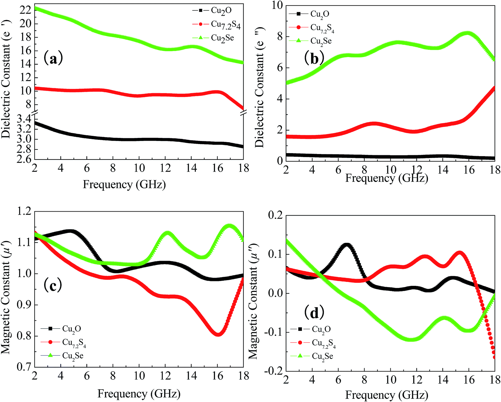 | ||
| Fig. 3 Dielectric constant and magnetic permeability of Cu2O, Cu7.2S4, and Cu2Se. Dielectric constant: real part (a) and imaginary part (b), and magnetic permeability: real part (c) and imaginary part (d). | ||
| Cu2O | Cu7.2S4 | Cu2Se | NiO | NiS | NiSe | |
|---|---|---|---|---|---|---|
| ε′ | 3.32 | 10.45 | 22.35 | 3.18 | 14.09 | 18.61 |
| ε′′ | 0.3 | 4.8 | 8.21 | 1.20 | 4.71 | 13.35 |
| μ′ | 0.12 | 0.10 | 0.14 | 1.48 | 1.28 | 1.29 |
| μ′′ | 1.13 | 1.13 | 1.16 | 0.07 | 0.10 | 0.06 |
| tanδE |
0.12 | 0.63 | 0.54 | 0.43 | 0.51 | 1.00 |
| tanδM |
0.12 | 0.13 | 0.12 | 0.08 | 0.16 | 0.09 |
| RL (dB) | −3.67 | −36.60 | −27.50 | −12.68 | −31.93 | −41.22 |
The ε′ value for NiO was stable (around 3) while the ε′ value decreased from 14.09 to 8.66 for NiS (Fig. 4a). There was a resonance peak of ε′ with a value of 18.61 at 9.76 GHz for NiSe. Pure NiS has both ferromagnetic ordering and paramagnetic domains.43 Minimal and maximal values of ε′ were found for NiO and NiSe. The ε′′ values had the same trends, increasing at the beginning and going down afterwards with the increase of frequency for NiO, NiS, and NiSe, resulting in the resonance peaks (Fig. 4b). The ε′′ value of NiSe resonance peak was 13.35 at 12.32 GHz, higher than that of NiO and NiS, indicating the loss was strongest and the anisotropicity was best for NiSe. The μ′ values of Ni chalcogenides were relatively close to 1 (Fig. 4c and d), while the μ′′ values for NiO, NiS, and NiSe decreased gradually. For NiO, NiS, and NiSe, the μ′ and μ′′ values are smaller than the ε′ and ε′′ values, with those of NiS and NiSe differ by an order of magnitude.
 | ||
| Fig. 4 Dielectric constant and magnetic permeability of NiO, NiS and NiSe. Dielectric constant: real part (a) and imaginary part (b), and magnetic permeability: real part (c) and imaginary part (d). | ||
The dielectric loss tanδE of Cu2Se, Cu7.2S4, and Cu2O decreased gradually, indicating Cu2Se had a better ability of dielectric loss compared with Cu2O and Cu7.2S4, allowing for the space charge polarization because of the increase in radius of O, S, and Se (Fig. 5a). Furthermore, Cu2O and Cu7.2S4 were obviously porous spherical aggregates but Cu2Se had lamellar structure (Fig. 2). The porous structure could reduce the effective dielectric constant and facilitates impedance matching.60 The dielectric loss tanδE of NiO, NiS, and NiSe was greater than the magnetic loss tanδM, thus, the dominant mechanism of the materials for EM absorption is the dielectric loss (Fig. 5c and d). Dielectric loss is mainly based on polarization relaxation, including interfacial polarization, molecular polarization, ionic polarization, and electronic polarization. The interfacial polarization always takes place in materials comprised of more than one phase composites. This polarization occurring at the interfaces is due to the migration of charge carriers through different dielectric properties of the composite material, which results in charge accumulation at the interfaces.61 The ionic polarization was stronger on account for the higher of the negative charge, the greater of the radius, and the greater of the distortion.
 | ||
| Fig. 5 Dielectric loss tangent (a) and magnetic loss tangent (b) of CuO, Cu7.2S4, and Cu2Se. Dielectric loss tangent (c) and magnetic loss tangent (d) of NiO, NiS, and NiSe. | ||
To evaluate the EM properties, the RL of samples with a particular thickness at frequency of 2–18 GHz was calculated using eqn (2) and (3) (Fig. 6). When the RL value was less than −10 and −20 dB, the EM wave absorption reached more than 90% (ref. 62) and 99% accordingly.63 Cu7.2S4 and Cu2Se exhibited good EM absorption properties (Fig. 6a–c). For Cu7.2S4, the minimum RL, the absorption peak frequency (APF), and the bandwidth when RL < −10 were −36.60 dB, 17.2 GHz, and 6 GHz when the thickness of the sample was 1.6 mm. For Cu2Se, the minimum RL, the APF, and the bandwidth of were −27.5 dB, 11.76 GHz, and 3 GHz, respectively when the thickness of the sample was 1.5 mm. Although these values are inferior to the RL of −54.5 dB at 11.4 GHz for CuS nanoflakes vertically aligned on graphene with a sample thickness of 2.5 mm,40 the bandwidth could be as wide as 6 GHz, and could extend beyond 18 GHz for Cu7.2S4 (Fig. 6b). For selenides, the only reported material was MnSe2 with a RL value of −12 dB at 12.72 GHz with a bandwidth of 2 GHz.42 The Cu2Se synthesized in this study is much better than MnSe2 in terms of RL value and bandwidth (Fig. 6c).
 | ||
| Fig. 6 Microwave absorption properties of Cu2O (a), Cu7.2S4 (b), Cu2Se (c), NiO (d), NiS (e), and NiSe (f) in the frequency range of 2 to 18 GHz. | ||
Among the Cu chalcogenides, although Cu2O has a better impedance matching and less EM reflection interface, its dielectric loss and magnetic loss are relatively low, bringing about less losses of EM waves through the material, resulting in poor absorption of microwave. Cu7.2S4 has a better impedance matching performance than Cu2Se, resulting in a superior reflection loss than Cu2Se.
The RL curves of NiO, NiS, and NiSe with specific thickness at 2–18 GHz were shown in Fig. 6d–f, respectively. The minimum RL of NiO was −12.68 dB at the APF of 12.80 GHz at a sample thickness of 4.5 mm with a narrow bandwidth (Fig. 6d). The minimum RL of NiS was −31.93 dB at the APF of 7.52 GHz with the thickness of 3 mm, and a bandwidth of 2 GHz (Fig. 6e). The RL value of NiSe at a thickness of 2.2 mm could achieve −41.22 dB (more than 99.99%) at the APF of 8.24 GHz (Fig. 6f). These results are comparable or better than those for NiO coated glass-ceramic tile,34 Ni–B coated Fe3O4,32 microporous Ni/NiO nanoparticles,33 and are much better than those of Ni coating on carbon fiber.31
Overall, the EM absorption performance of NiSe was much better than that of NiO and NiS. Excellent microwave absorbing materials needed high dielectric loss and magnetic loss, while the good impedance matching is more important.64,65 The dielectric constant and magnetic permeability of NiO were the smallest among the three, therefore, only less energy was kept and wore-down after EM waves penetrate into the material. Weak dielectric loss and magnetic loss caused the inferior EM wave-absorbing effect of NiO. Because dielectric loss was larger and the matching impedance was closer to 1, NiSe was a better microwave absorbing material than NiS. Comparing the EM absorbing parameters (ε′, ε′′, μ′, μ′′, tanδE, tanδM, and the RL) of the six samples (Table 1), it can be found that the RL value of NiSe with a thickness of 2.2 mm could achieve the minimum value −41.22 dB at the APF of 8.24 GHz among the six samples. The tanδE could achieve almost 1. The tanδE is greater than tanδM, thus the dominant mechanism of EM absorption is due to the dielectric loss. The RL value of Cu7.2S4 is just smaller than that of NiSe among the rest five samples, illustrating it is also a favourable EM absorbing material. The minimum RL, the APF, and the bandwidth of Cu7.2S4 were −36.60 dB, 17.2 GHz, and 6 GHz when the thickness of the sample was 1.6 mm. The tanδE value is also greater than that of tanδE, confirming that the dielectric loss is the main mechanism for EM absorption. Among the rest four samples, except Cu2O, the other three are all better microwave absorbing materials, and the dielectric loss is the primarily mechanism of their EM absorption. In contrast to copper and nickel compounds with different anions, we have found that the absorption properties of the oxides (Cu2O, NiO) are not as good as those of sulphides and selenides, as compared with the same parent oxyacids. Such as copper chalcogenides, the hollow structure can increase its absorption properties, it can enhance the microwave absorbing properties with the hollow spherical shape of the size reducing. However, Cu2Se is sheet-like structure and its microwave absorbing properties reduce slightly. The structure of the nickel chalcogenides is petal-like shape. It can be found that the microwave absorption performance improved significantly with its size be smaller. The absorption performance of NiSe is the best.
It can be found that the thickness of the absorbers is one of important factors, which affects the RL values and location of optimal RL.66,67 As the thickness of sample increasing, the matching frequency (fm) gradually moved towards the lower frequency.68,69 The results matched well with the quarter wavelength (L/4) model which is submitted by relevant reports:
 | (4) |
4. Conclusion
The Cu2O, Cu7.2S4, Cu2Se, NiO, NiS, and NiSe were synthesized through a hydrothermal method, and the composites used for microwave absorption measurement were prepared by mixing them (50%) with paraffin matrix (50%). The results showed that all composites had high capability for microwave absorption, except Cu2O. The microwave-absorbing performance enhanced with an increase in anionic radii of the materials, which could be attributed to the effect of space charge polarizations.The microwave response spectrum could be controlled by adjusting the thickness of the samples to improve the application of materials under different frequencies. Excellent microwave absorption materials possessed two conditions: better matching impedance, which could decrease the reflectivity of materials, and higher dielectric loss and magnetic loss, which could improve the absorbing property of materials. While the thickness of Cu7.2S4–paraffin composite was 1.6 mm, the minimum RL (−36.6 dB) appeared at the APF of 17.2 GHz, and the bandwidth for RL < −10 dB (the microwave absorption is more than 90%) was 6 GHz. The thickness of NiO–paraffin composite was 3 mm, the minimum RL (−31.93 dB) appeared at the APF of 7.52 GHz, and the bandwidth was 2 GHz. For Cu2Se–paraffin composite, with a thickness of 1.5 mm, the minimum RL was −27.5 dB at the APF of 11.76 GHz, and the bandwidth was 3 GHz. While for NiSe–paraffin composite with a thickness of 2.2 mm, the minimum RL was −41.22 dB at the APF of 8.24 GHz, and the bandwidth was 1.6 GHz.
The results from this research demonstrated in the first time the applicability and feasibility of Cu and Ni chalcogenides to be used as EM absorbing materials with excellent response and performance. Our further research will be focused on coating these materials on nanofibers and graphenes.
Acknowledgements
This research was jointly supported by National Natural Science Foundation of China (51604248), International S & T Cooperation (S2014ZR0062), Beijing Natural Science Foundation (2153041) and the Fundamental Research Funds for the Central Universities (53200859447).References
- N. Li, M. H. Cao and C. W. Hu, J. Mater. Chem., 2012, 22, 18426–18432 RSC.
- N. Leitgeb and J. Schrottner, Bioelectromagnetics, 2003, 24, 387–394 CrossRef PubMed.
- S. Sivani and D. Sudarsanam, Biol. Med., 2012, 4, 202–216 Search PubMed.
- A. G. Whittaker and D. M. P. Mingos, Dalton Trans., 2002, 3967–3970 RSC.
- X. B. Xing, G. C. Lv, W. Xu, L. B. Liao, W. T. Jiang, Z. H. Li and G. S. Wang, RSC Adv., 2016, 6, 58844–58853 RSC.
- W. Xu, G. C. Lv, X. B. Xing, X. J. Zhang and G. S. Wang, Sci. Adv. Mater., 2016, 8, 966–971 CrossRef CAS.
- H. F. Li, J. Wang, Y. H. Huang, X. Q. Yan, J. J. Qi, J. Liu and Y. Zhang, Mater. Sci. Eng., B, 2010, 17, 81–85 CrossRef.
- R. J. Aitke, L. E. Bennetts, D. Sawyer, A. M. Wiklendt and B. V. King, Int. J. Androl., 2005, 28, 171–179 CrossRef PubMed.
- S. J. Genuis, Public Health, 2008, 2, 113–124 CrossRef PubMed.
- M. Maeda, S. S. Satoshi, T. Kagotani, N. Tezuka and K. Inomata, J. Magn. Magn. Mater., 2004, 281, 195–205 CrossRef.
- X. J. Zhang, G. C. Lv, G. S. Wang, T. Y. Bai, J. K. Qu, X. F. Liu and P. G. Yin, RSC Adv., 2015, 5, 55468–55473 RSC.
- M. N. Afsar, Z. J. Li, K. A. Korolev, A. Namai and S. I. Ohkoshi, IEEE Trans. Magn., 2011, 47, 333–336 CrossRef CAS.
- A. K. Tagantsev, V. O. Sheman, K. F. Astafiev, J. Venkatesh and N. Setter, J. Electroceram., 2003, 11, 5–66 CrossRef CAS.
- A. K. Tagantsev and K. F. Astafiev, Integr. Ferroelectr., 2001, 39, 251–260 CrossRef.
- B. Zhao, G. Shao, B. B. Fan, W. Y. Zhao and R. Zhang, Phys. Chem. Chem. Phys., 2015, 17, 6044–6052 RSC.
- C. Y. Liang, C. Y. Liu, H. Wang, L. Wu, Z. H. Jiang, Y. Q. Xu, B. Z. Shen and Z. J. Wang, J. Mater. Chem. A, 2014, 2, 16397–16402 CAS.
- W. W. Liu, H. Li, Q. P. Zeng, H. N. Duan, Y. P. Guo, X. F. Liu, C. Y. Sun and H. Z. Liu, J. Mater. Chem. A, 2015, 3, 3739–3747 CAS.
- C. M. Yang, H. Y. Li, D. B. Xiong and Z. Y. Cao, React. Funct. Polym., 2009, 69, 137–144 CrossRef CAS.
- X. L. Zheng, J. Feng, Y. Zong, H. Mao, X. Y. Hu, J. T. Bai and X. H. Li, J. Mater. Chem. C, 2015, 3, 4452–4463 RSC.
- J. Xiang, J. L. Li, X. H. Zhang, Q. Ye, J. H. Xu and X. Q. Shen, J. Mater. Chem. A, 2014, 2, 16905–16914 CAS.
- R. C. Che, L. M. Peng, X. F. Duan, Q. Chen and X. L. Liang, Adv. Mater., 2004, 16, 401–405 CrossRef CAS.
- X. C. Zhao, Z. M. Zhang, L. Y. Wang, K. Xi, Q. Q. Cao, D. H. Wang, Y. Yang and Y. W. Du, Sci. Rep., 2013, 3, 1–5 Search PubMed.
- J. Zeng, J. C. Xu, P. Tao and W. Hua, J. Alloys Compd., 2009, 487, 304–308 CrossRef CAS.
- J. Zeng, H. Q. Fan, Y. L. Wang, S. Q. Zhang, J. Xue and X. Y. Cheng, Thin Solid Films, 2012, 520, 5053–5059 CrossRef.
- Y. Z. Wan, T. Cui, J. Xiao, G. Y. Xiong, R. S. Guo and H. L. Luo, J. Alloys Compd., 2016, 687, 334–341 CrossRef CAS.
- X. Y. Wang, G. C. Lv, L. B. Liao and G. S. Wang, RSC Adv., 2015, 5, 55595–55601 RSC.
- G. S. Wang, L. Z. Nie and S. H. Yu, RSC Adv., 2012, 15, 6216–6221 RSC.
- G. Tong, Q. Hu, W. H. Wu, W. Li, H. S. Qian and Y. Liang, J. Mater. Chem., 2012, 22, 17494–17504 RSC.
- C. H. Gong, J. W. Zhang, X. F. Zhang, L. G. Yu, P. Y. Zhang, Z. S. Wu and Z. J. Zhang, J. Phys. Chem. C, 2010, 114, 10101–10107 CAS.
- C. Wang, X. J. Han, P. Xu, J. Y. Wang, Y. C. Du, X. H. Wang, W. Qin and T. Zhang, J. Phys. Chem. C, 2010, 114, 3196–3203 CAS.
- Y. Z. Fan, H. B. Yang, X. Z. Liu, H. Y. Zhu and G. T. Zou, J. Alloys Compd., 2008, 461, 490–494 CrossRef CAS.
- X. Li, X. Han, Y. Tan and P. Xu, J. Alloys Compd., 2008, 464, 352–356 CrossRef CAS.
- T. Liu, Y. Pang, X. B. Xie, W. Qi, Y. Wu, S. Kobashi, J. Zheng and X. G. Li, J. Alloys Compd., 2016, 667, 287–296 CrossRef CAS.
- R. Yao, S. Y. Liao, X. Y. Chen, G. N. Tang, G. R. Wang and F. Zheng, Ceram. Int., 2016, 42, 8179–8189 CrossRef CAS.
- Z. G. An and J. J. Zhang, Dalton Trans., 2016, 45, 2881–2887 RSC.
- Z. G. An, J. J. Zhang and S. L. Pan, Dalton Trans., 2010, 39, 3378–3383 RSC.
- K. Z. Du, A. Chaturvedi, X. Z. Wang, Y. Zhao, K. K. Zhang, M. I. Utama, P. Hu, H. Jiang, Q. H. Xiong and C. Kioc, Dalton Trans., 2015, 44, 13444–13449 RSC.
- Z. F. Zhao, X. J. Liu, G. Y. Deng, F. Zhou, L. J. Zhang, Q. Wang and L. Lu, Dalton Trans., 2016, 45, 13456–13465 RSC.
- X. A. Li, B. Zhang, C. H. Ju, X. J. Han, Y. C. Du and P. Xu, J. Phys. Chem. C, 2011, 115, 12350–12357 CAS.
- P. B. Liu, Y. Huang, J. Yan, Y. W. Yang and Y. Zhao, ACS Appl. Mater. Interfaces, 2016, 8, 5536–5546 CAS.
- B. Zhao, G. Shao, B. B. Fan, W. Y. Zhao, S. H. Zhang, K. K. Guan and R. Zhang, J. Mater. Chem. C, 2015, 3, 10862–10869 RSC.
- J. Zhang, J. W. Liu, C. Y. Liang, F. Zhang and R. C. Che, J. Alloys Compd., 2013, 548, 13–17 CrossRef CAS.
- E. C. Linganiso, B. W. Mwakikunga, N. J. Coville and S. D. Mhlanga, J. Alloys Compd., 2015, 629, 131–139 CrossRef CAS.
- W. D. Xiang, H. J. Zhao, J. S. Zhong, Y. Q. Guo, Z. P. Chen, H. Y. Luo, X. L. Zhao, X. J. Liang and X. Q. Yang, J. Non-Cryst. Solids, 2012, 358, 2641–2649 CrossRef CAS.
- M. K. Mehdi, Z. Zabihullah and S. N. Masoud, J. Phys. Chem. C, 2016, 120, 2096–2108 Search PubMed.
- S. L. Liu, Z. S. Zhang, J. C. Bao, Y. Q. Lan, W. W. Tu, M. Han and Z. H. Dai, J. Phys. Chem. C, 2013, 117, 15164–15173 CAS.
- L. Zhang, S. L. Zhao, Y. F. Li, Y. Q. Lan, M. Han, Z. H. Dai and J. C. Bao, Eur. J. Inorg. Chem., 2015, 2229–2236 CrossRef CAS.
- X. Sun, J. P. He, G. X. Li, J. Tang, T. Wang, Y. X. Guo and H. R. Xue, J. Mater. Chem. C, 2013, 4, 765–777 RSC.
- G. Z. Wang, Z. Gao, S. W. Tang, C. Q. Chen, F. F. Duan, S. C. Zhao, S. W. Lin, Y. H. Feng, L. Zhou and Y. Qin, ACS Nano, 2012, 6, 11009–11017 CrossRef CAS PubMed.
- A. F. Oskooi, D. Roundy, M. H. Ibanescu, P. Bermei, J. D. Joannopoulos and S. G. Johnson, Comput. Phys. Commun., 2010, 181, 687–702 CrossRef CAS.
- C. M. Watts, X. L. Liu and W. J. Padilla, Adv. Mater., 2012, 24, 98–120 Search PubMed.
- A. Drmota, J. Koselj, M. Drofenik and A. Znidarsic, J. Magn. Magn. Mater., 2012, 324, 1225–1229 CrossRef CAS.
- R. C. Che, X. F. Duan, Q. Chen and X. L. Liang, Adv. Mater., 2004, 16, 401–405 CrossRef CAS.
- J. W. Liu, R. C. Che, H. J. Chen, F. Zhang, F. Xia, Q. S. Wu and M. Wang, Small, 2012, 8, 1214–1221 CrossRef CAS PubMed.
- X. Cao, W. J. Chiang, Y. C. King and Y. K. Lee, IEEE. Trans. Power. Electron., 2007, 22, 679–685 CrossRef.
- B. Zhao, G. Shao, B. B. Fan, W. Y. Zhao, Y. Q. Chen and R. Zhang, RSC Adv., 2015, 5, 9806–9814 RSC.
- Q. M. Su, J. Li, Z. Guo, G. H. Du and B. S. Xu, J. Phys. Chem. C, 2011, 115, 1838–1842 CAS.
- J. Zheng, H. L. Lv, X. H. Lin, G. B. Jin, X. G. Li and Y. W. Du, J. Alloys Compd., 2014, 589, 174–181 CrossRef CAS.
- X. W. Yin, L. Kong, L. T. Zhang, L. F. Cheng, N. H. Travitzky and P. Greil, Int. Mater. Rev., 2014, 59, 326–355 CAS.
- X. L. Li, Z. Bin, C. H. Ju, X. J. Han, Y. C. Du and P. Xu, J. Phys. Chem. C, 2011, 15, 12350–12357 Search PubMed.
- B. Zhao, G. Shao, B. B. Fan and W. Y. Zhao, J. Mater. Chem. A, 2015, 3, 10345–10352 CAS.
- B. Zhao, B. B. Fan, G. Shao and W. Y. Zhao, ACS Appl. Mater. Interfaces, 2015, 7, 18815–18823 CAS.
- Y. Y. Lv, Y. T. Wang, H. L. Li, Y. Lin, Z. Y. Jiang, Z. X. Xie, Q. Kuang and L. S. Zheng, ACS Appl. Mater. Interfaces, 2015, 7, 13604–13611 Search PubMed.
- M. Zhou, X. Zhang, J. M. Zhao, S. L. Zhao, L. Wang and B. X. Feng, J. Phys. Chem. C, 2011, 115, 1398–1402 CAS.
- S. M. Abbas and R. Chatterjee, J. Appl. Phys., 2007, 101, 1–5 CrossRef.
- B. B. Zhao, B. B. Fan, Y. W. Xu and G. Shao, ACS Appl. Mater. Interfaces, 2015, 7, 26217–26225 CAS.
- B. Zhao, G. Shao, B. B. Fan and W. Y. Zhao, RSC Adv., 2014, 4, 61219–61225 CAS.
- T. Inui, K. Konishi and K. Oda, IEEE Trans. Magn., 1999, 35, 3148–3150 CrossRef.
- I. Kong, S. H. Ahmad, M. H. Abdullah, D. Hui, A. N. Yusoff and D. Puryanti, J. Magn. Magn. Mater., 2010, 322, 3401–3409 CrossRef CAS.
| This journal is © The Royal Society of Chemistry 2016 |