
 Open Access Article
 This Open Access Article is licensed under a Creative Commons Attribution-Non Commercial 3.0 Unported Licence
Angle-tunable polymeric photonic diode with 1D-photonic crystal for enhanced light control†
Jaismon
Francis‡
 ,
Nikhil
Puthiya Purayil‡§
,
Chandrasekharan
Keloth
and
C. S.
Suchand Sangeeth
*
,
Nikhil
Puthiya Purayil‡§
,
Chandrasekharan
Keloth
and
C. S.
Suchand Sangeeth
*
Department of Physics, National Institute of Technology Calicut, Kerala 673601, India. E-mail: sangeeth@nitc.ac.in
First published on 7th August 2024
Abstract
Integrated optical circuits depend on optical diodes for passive nonreciprocal light transmission. The realization of optical diode action remains a significant challenge in nanophotonics, with conventional approaches often relying on non-compact and expensive magneto and electro-optic isolators. This work presents an all-polymeric optical diode based on the principle of asymmetric nonlinear absorption in the nonlinear regime. In contrast to earlier diodes employing this principle, this diode architecture offers a simplified fabrication process, exhibits a compact footprint, and eliminates the need for a liquid phase. The attained optical diode consists of a simple structure employing PEDOT:PSS as a saturable absorber medium and a 1-dimensional polymeric photonic crystal (PhC) structure consisting of gold–carbon core–shell nanostructures (Au@C NS) as a reverse saturable absorber medium. Integration of the active medium into a PhC architecture provides a unique avenue for engineering light–matter interactions, resulting in angle-tunable optical diode activity. This device exhibits all-optical diode action with no phase-matching constraints. Our structure exhibits a nonreciprocity factor of up to ∼12.5 dB, achieved through a facile and cost-effective fabrication method. This promising combination makes this system a potential candidate for developing compact photonic integrated devices.
1. Introduction
Optical nonreciprocal devices, such as isolators, circulators, and optical diodes, are critical components for photonic integrated circuits (PICs). These devices enable directional control of light propagation, a key functionality for various PIC applications.1–3 These devices are fundamental for achieving high-performance photonics and optical communication systems.4 Most of the available nonreciprocal optical elements rely on magneto-optical materials, they usually need bulky external magnetic fields for operation.5 Moreover, the requirement of bulk optical media for obtaining strong magneto-optical response hinders the miniaturization and integration into PICs.6 To overcome these issues, alternate approaches have been proposed and demonstrated through various photonic architectures such as optical resonators,5 metamaterials,7 photonic crystals,8–10 electro-tunable liquid crystals,11,12 the opto-acoustic effects,13 or the thermo-optic effect.14 Despite their ingenuity, these approaches lack scalability and cost-effectiveness. Moreover, the operation of these devices requires the presence of magnetic and electric fields and the fulfillment of phase-matching conditions.5 Also, their performance is significantly influenced by the polarization of incident light. Hence, developing a simple structure for obtaining high contrast, passive nonreciprocal light transmission is crucial.15Nonreciprocal optical devices can be efficiently implemented by exploiting nonlinear optical (NLO) responses in materials. Placing a saturable absorber (SA) and a reverse saturable absorber (RSA) in the path of a light beam results in an intensity-sensitive unidirectional, diode-like transmission of light.16 These systems offer an affordable and easily manufacturable design, making them promising for advancing the field of optical computing and signal processing.3,17 The concept of an optical diode based on asymmetric nonlinear absorption was first proposed by R. Philip et al. in 2006.16 To create a jump discontinuity in the nonlinearity, they arranged a 3 mm thick orange-colored glass filter (SA medium) in tandem with cobalt phthalocyanine (RSA medium) taken in a glass cuvette of thickness 1 mm. Although this device has exhibited optical diode action at 532 nm wavelength, the lack of compactness and liquid phase operation are major drawbacks. In 2010, B. Anand et al. developed a solid-state all-carbon passive optical diode using a few-layer graphene (FLG) and bilayer graphene (BLG) saturable absorber and fullerene (C60) as a reverse saturable absorber.3 The attractiveness of this ultra-compact optical diode was its low operating volume, large bandwidth, and chemical and thermal stability. However, one of the disadvantages of this diode is that it requires relatively complex chemical vapor deposition technology to make BLG and FLG layers. Thus, enabling an optical diode in a highly flexible, cost-effective, solution-processable, and printable material is crucial. In addition to conventional materials,18,19 recent research has explored a range of novel materials for optical diodes, including 2D-MXene films,20 2D-tellurium,21 GeSe nanoplates,22 2D graphdiyne,23 Franckeite,24 Boron quantum dots,25 and combinations of perovskites with transparent conducting oxides.26
A significant limitation of conventional nonlinear optical materials is the need for highly intense laser pulses to invoke nonlinear responses. The nonlinear optical response in materials is inherently weak since governed by the photon–photon interactions mediated by the material electronic transitions.27 Since the nonlinear processes are superlinearly dependent on the interacting electromagnetic field, high operational power is required and this hinders the practical photonic applications. The NLO materials incorporated in engineered photonic architectures having subwavelength scales are identified as suitable platforms for nanophotonic applications.28 Nanoscale photonic structures provide suitable light confinement required to induce the nonlinear response of embedded materials even in relatively low input threshold laser beams. Thus, such nanoscale architectures can be able to provide light-induced changes in the materials more perceptible.29 A photonic crystal (PhC) is a periodic dielectric structure that serves as a suitable platform to enhance and manipulate the nonlinear response in materials.30 Tremendous progress has been achieved in incorporating nonlinear media in PhCs having unparalleled capabilities in tailoring the light–matter interactions and thereby unlocking new device applications.
Organic semiconductors (OSCs) consist of a diverse group of carbon-based materials that exhibit semiconductive behavior. They have electrical and optical properties similar to their inorganic counterparts. These materials, which include small molecules and conjugated polymers (CPs), have enabled the development of various organic electronic devices. Examples of such devices are light-emitting diodes, organic field-effect transistors, organic solar cells, etc.31–33 CPs with tunable electrical properties offer promising potential for NLO applications, including switching, optical frequency conversion, and epsilon-near-zero (ENZ) material.34–36 Poly(3,4-ethylenedioxythiophene) polystyrene sulfonate (PEDOT:PSS) is a conductive polymer that has emerged as a benchmark material in organic electronics due to its unique combination of transparency, conductivity, flexibility, and ease of processing.37,38 PEDOT:PSS is extensively used in organic electronics with applications in photovoltaic cells, organic memories, electrochromic devices, organic transistors energy conversion and storage devices, etc.39–41 The high density of delocalized π molecular orbital electrons in the PEDOT backbone makes it a promising fast responding material suitable for application in nonlinear optical elements. The preparation and thickness optimization of PEDOT:PSS films are well-established and extensively documented in the literature.37 Few studies have investigated the nonlinear optical capabilities of PEDOT:PSS, yet the applications of the system have not yet been explored.42,43
In this work, nonreciprocal light propagation, a characteristic of optical diodes, is realized in a straightforward configuration comprising a saturable absorber medium of PEDOT:PSS and a one-dimensional PhC embedded with gold–carbon core–shell nanostructures (Au@C) in alternative layers as a reverse saturable absorber. The PhC serving as the RSA layer was fabricated using the spin coating technique. The PhC structure consists of 10 bilayers and was fabricated using poly(9-vinylcarbazole) (PVK) and cellulose acetate (CA). The band edge of the PhC was designed to match the excitation wavelength to achieve optimal light confinement through the slow light effect. This confinement, known as the photonic band edge (PBE) effect, significantly reduces the group velocity of light near the PBEs. The slow light effect enhances the interaction between light and the active medium (Au@C) in the alternative layers of PhC, leading to improved RSA. Details of the fabrication and nonlinear optical characterization of this PhC structure are presented elsewhere.44 Integrating the active medium into a PhC architecture provides a unique avenue for engineering light–matter interactions, resulting in angle tunable optical diode activity. Nonlinear optical characterization was conducted using the Z-scan technique, utilizing a Q-switched Nd:YAG laser emitting 7 ns pulses at 532 nm. Our structure exhibits a nonreciprocity factor of up to ∼12.5 dB, achieved through a facile, cost-effective fabrication method. This unique combination makes this system a promising platform for developing compact photonic integrated devices.
2. Experimental section
2.1. Materials
Commercially available PVK (molecular weight = 1![[thin space (1/6-em)]](https://www.rsc.org/images/entities/char_2009.gif) 100000), CA (molecular weight = 100000), and PEDOT:PSS (1.3 wt% dispersion in H2O) were purchased from Sigma-Aldrich. Au@C were synthesized using pulsed laser (Nd:YAG laser operating at 532 nm wavelength, 7 ns pulse width, and 10 Hz repetition rate) irradiation in chlorobenzene. Subsequently, Au@C nanostructures were incorporated into the PVK matrix. The schematic of the laser ablation setup is given in Fig. 1 and details are provided in ref. 45.
100000), CA (molecular weight = 100000), and PEDOT:PSS (1.3 wt% dispersion in H2O) were purchased from Sigma-Aldrich. Au@C were synthesized using pulsed laser (Nd:YAG laser operating at 532 nm wavelength, 7 ns pulse width, and 10 Hz repetition rate) irradiation in chlorobenzene. Subsequently, Au@C nanostructures were incorporated into the PVK matrix. The schematic of the laser ablation setup is given in Fig. 1 and details are provided in ref. 45.
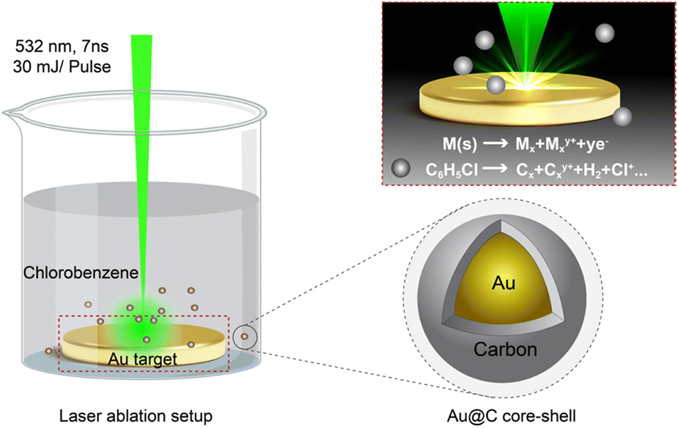 | ||
| Fig. 1 The laser ablation synthesis of Au@C core–shell nanostructures. | ||
2.2. Fabrication of PEDOT:PSS/PhC optical diode
1D-PhC was fabricated via spin coating on glass substrates. A 3.0 wt% solution of PVK dispersed with synthesized Au@C was prepared and sonicated to ensure homogeneity. For CA, a 2.50 wt% solution in diacetone alcohol was used. Alternating layers of PVK (72 nm) and CA (83 nm) were spin coated, followed by thermal annealing at 110 °C for 20 minutes to optimize film quality (see Fig. 2). The spin coating process was carried out using a Laurell WS-650MZ-23NPPB spin coater. Spin speeds were varied from 2300 to 2550 rpm to achieve the desired film thickness. A saturable absorber layer, crucial for the optical diode, was prepared by drop-casting a 1.3 wt% PEDOT:PSS solution onto a glass substrate. To enhance wettability, the glass surface was subjected to oxygen plasma treatment for 30 seconds before coating. Following drop-casting, the PEDOT:PSS layer was annealed at 70 °C for 60 minutes. Employing a stylus profilometer, the final layer thickness was determined to be 3.1 μm. The RSA medium of the optical diode was a PhC, fabricated as detailed in Fig. 2.44 | ||
| Fig. 2 (a) Fabrication of PhC using the spin coating technique. (b) Schematic of the PEDOT:PSS/PhC optical diode fabricated in this study. | ||
2.3. Characterization
The nonlinear optical properties of PhC and PEDOT:PSS were characterized using the open-aperture Z-scan. A Q-switched Nd:YAG laser served as the light source, emitting 7 ns pulses at 532 nm with a 10 Hz repetition rate. The output polarization of this laser system is vertically polarized. The laser beam was focused onto the sample using a convex lens (focal length: 15 cm). The sample was moved across the focal plane of the lens using a computer-controlled translation stage with a 1 mm step size. Transmitted energy through the sample was measured by a pyroelectric detector-based energy ratio meter (RJP-735 & Rj-7620, Laser Probe Inc.). The normalized transmittance data was subsequently fitted numerically to the relevant propagation equation to extract the nonlinear absorption coefficients. The Z-scan experimental setup was calibrated using CS2 to ensure accurate NLO measurements. The detailed experimental setup and procedure of the Z-scan are described in our previous reports.453. Results and discussion
3.1. Optical properties of the polymer PhC
The optical response of the nonlinear PhCs is mainly influenced by their photonic band structure. Engineered defect states in PhCs can confine light, resulting in enhanced linear and nonlinear optical properties of active materials incorporated within them. Depending on their structural characteristics, various techniques can be employed to achieve spatial confinement of optical fields in PhCs. A widely adopted method involves the creation of cavities consisting of a nonlinear active medium with a half-wavelength optical thickness.30 The losses resulting from the absorbent media within the cavity make these devices very challenging to fabricate.46 Instead of being used as a cavity layer, the nonlinear media can be used as one of the constituent layers of the PhC. The excitation of photonic band-edge modes leads to the localization of electromagnetic energy in these layers and thereby improves the nonlinear effects considerably.47 To demonstrate this approach, a 1D PhC is fabricated, integrating Au@C core–shell nanostructures within alternating layers. The PhC is specifically engineered to ensure that the laser wavelength coincides precisely at the edge of the stop band. The details of fabrication are provided under the Experimental section. The normal incidence reflectance spectrum shows a peak with reflectance close to 75% at 2.54 eV, which corresponds to 488 nm (see Fig. 3(a)). The incorporated Au@C (see Fig. S1 in ESI†) exhibited negligible linear absorption at these photon energies. This ensures that the reflectance profile of the PhC is unaffected by the presence of Au@C. The band edge modes are observed at 2.33 eV and 2.77 eV on either side of the reflectance peak, consistent with expectations. Electromagnetic energy is stored in the alternating dielectric layers of the PhC when it is excited with a frequency near the band edge modes.47,48 To illustrate this effect, we have carried out the transfer matrix analysis to compute the electric field profiles inside the structure at three distinct photon energies as shown in Fig. 3(b). The photon energies 2.33 eV and 2.77 eV correspond to the low and high-frequency band edge modes and 2.54 eV is an energy value lying inside the stop band. The red solid lines in Fig. 3(b) present the refractive index (R.I.) profile of the PhC. The R.I. values of the alternative layers (PVK, n = 1.68, and CA, n = 1.47), are explicitly labeled on the right y-axis. The R.I. profiles are superimposed to demonstrate the field confinement in the structure. While illuminating the structure with photons of energy values lying within the stop band region, the field distribution shows an oscillatory decaying profile, whereas the excitation of both band edge modes shows enhanced field amplitudes. When the structure is excited with light of energy equal to the high energy band edge mode, the electric fields are maximum at the lower refractive index region of the PhC layers. In contrast, if the excitation photon energy matches with the lower energy band edge mode, the field is concentrated at the high refractive index regions of the structure. So, by careful design of the band edge modes, we can achieve enhanced field amplitudes at the NLO material incorporated layers. Since the laser excitation spectrally coincides with the low-energy band-edge mode, the field is maximized in the high dielectric region (PVK). The Au@C nanostructures are doped in the PVK layers, to boost their nonlinear optical properties by enhancing light–matter interaction. | ||
| Fig. 3 (a) The reflectance spectra of the PhC recorded at normal incidence. (b) The field profiles (blue solid lines) inside the PhC on exciting with different photon energies: 2.33 eV (low energy band edge), 2.54 eV (photon energy lying in the stop band region), and 2.77 eV (high energy band edge). The refractive index (R. I.) is represented by red solid lines. (c) The angle-resolved transmission contour plot for p-polarized light. The color bar represents the transmittance values. | ||
TM-polarised angle-resolved transmission spectroscopy is used to map the stop band different incident angles.44Fig. 3(c) depicts the experimental angle-resolved transmission spectrum of the PhC for photon energies 1.37 eV to 3.54 eV. The incidence angle is varied from normal to 80° with a 2° increment with the help of a goniometer. From the experimental transmission color map, it is evident that the photonic stop band blue shifts as the angle of incidence increases, as governed by Bragg's law.49 The normal incidence transmission spectrum and angular dispersion of stopband under TM-polarization are also simulated using the transfer matrix method (see Fig. S2 in ESI†) and compared with the experimental data. The normal-incidence transmittance spectrum of a ten-bilayer PVK/CA multilayer thin film was calculated using the transfer matrix method and given in Fig. S3 (ESI†). The consistency of experimental and theoretical data confirms the high homogeneity of spin-casted polymer layers and the quality of the fabricated PhC.
The open aperture Z-scan experiments with 7 ns laser pulse at 532 nm were carried out to study the nonlinear optical properties of the PhC structure. Fig. 4(a) displays the experimental Z-scan data at an on-axis peak intensity of 1.4 × 10¹² W m−2. Nonlinear transmittance decreases as the sample approaches the focal point, with data points exhibiting symmetry around the z = 0, suggesting reverse saturable absorption. Fig. 4(b) shows the Z-scan data at an on-axis peak intensity of 7 × 10¹¹ W m−2. At this intensity, nonlinear transmission exhibits two humps at pre-focal and post-focal positions, suggesting a combination of feeble SA and RSA in the system. The PhC structure exhibited a linear transmittance of 90%. The transmitted intensity for a given input intensity is obtained by numerically solving the appropriate nonlinear pulse propagation equation a for a third-order nonlinear absorber, given by eqn (1).50,51 This approach is well-established for modeling various nonlinear optical processes, including two-photon absorption, saturable absorption, and excited-state absorption.16,50,52–54
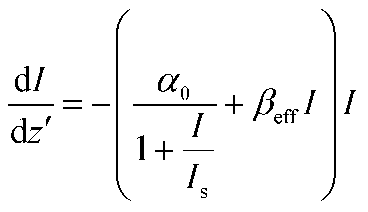 | (1) |
 | ||
| Fig. 4 (a) The open aperture Z-scan data of PhC at the on-axis peak intensity of 1.4 × 10¹² W m−2 and (b) Z-scan data at an on-axis peak intensity of 7 × 10¹¹ W m−2. | ||
The angle-dependent nonlinear transmission is shown in Fig. 5(a). The sample was mounted on a rotation stage and placed on a computer-controlled linear translation stage. The Z-scan experiments were conducted for various angles of incidence and the transmission minimum points (i.e., transmittance at z = 0) were plotted against the angle. The on-axis peak intensity is kept at 1.4 × 10¹² W m−2 during the angle-dependent Z-scan measurement. The nonlinear transmittance at focus (TNL) was measured across various angles of incidence, spanning from 0° to 50°. In the graph depicting the nonlinear transmittance of a sample as a function of the angle of incidence, the following observations were made: the lowest nonlinear transmission (high NLA) is observed at normal incidence and a sharp surge in the nonlinear transmittance is observed from 10 to 20 degrees. Beyond 20 degrees, the transmittance changes more gradually, indicating a less pronounced variation with increasing angle. This suggests that the sample exhibits a sharp nonlinear response at lower angles. The observed change in the NLA can be explained by the effective field distribution in the sample when exciting with resonant and off-resonant frequencies. At normal incidence, when the band-edge precisely aligns with the excitation wavelength (i.e., 532 nm), the highest overall field localization occurs within the high refractive index layers of the PhC.55 As the Au@C is embedded in the PVK matrix, the nonlinear media experiences the maximum field strength. Conversely, altering the incident angle results in a blue shift of the reflection band and the band edge modes, causing the excitation at 532 nm to become off-resonant. Consequently, this reduces the interaction with the Au@C, leading to lower nonlinear absorption. The decline in nonlinear transmittance from 20° to 50° can be attributed to the increased path length traversed by the excitation pulse. The simulated electric field amplitude in the PhC with respect to the angle of incidence for 532 nm excitation is given in Fig. 5(b). The change in the nonlinear transmittance shown in Fig. 5(a) is well correlated with the spatial electric field intensity mapping given in Fig. 5(b).
 | ||
| Fig. 5 (a) TNL (nonlinear transmittance at the focus for the on-axis peak intensity of 1.4 × 10¹² W m−2) of PhC at different angles of incidence. (b) Simulated electric field profile in the DBR as a function of external angle of incidences. | ||
3.2. PEDOT:PSS as saturable absorber
The PEDOT:PSS thin film was fabricated by drop-casting 1.3 wt% solution in water to a clean glass slide. The primary structure of the PEDOT:PSS is shown in Fig. 6(a). The UV-visible absorption spectrum of the PEDOT:PSS film is presented in Fig. 6(b). The sample shows faint absorption in the visible and broad absorption in the near IR spectral regions, which is attributed to the excitonic absorption related to the π–π* transition of PEDOT moiety. The distinctive peak observed at approximately 380 nm is a result of the transition from the n to π* states within the PEDOT. The extended absorption beyond 700 nm corresponds to the transitions of polarons and uncoupled bipolarons. Cross-sectional SEM was taken to find the thickness of the drop-casted film (Fig. 6(c)). It is found that the thickness of the film is approximately 3.1 μm.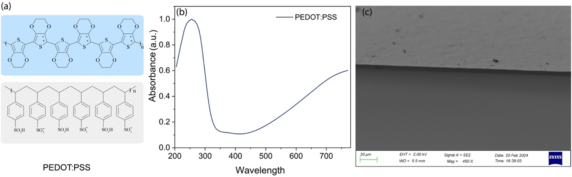 | ||
| Fig. 6 (a) Primary structure of PEDOT:PSS, (b) UV-visible absorption spectrum, (c) cross-sectional SEM. | ||
To investigate the nanosecond nonlinear absorption properties of the drop-casted PEDOT:PSS film, open-aperture (OA) Z-scan experiments were performed at various excitation intensities. The OA Z-scan trace obtained at on-axis peak intensity 2.8 × 10¹² W m−2, which corresponds to input laser energy of 20 μJ is shown in Fig. 7(a). The OA Z-scan data indicate the presence of a saturation effect. This is evident from the increased transmission, which reaches its maximum at z = 0, in contrast to the normalized linear transmittance. The Is value is obtained by fitting the experimental data to eqn (2).52,54
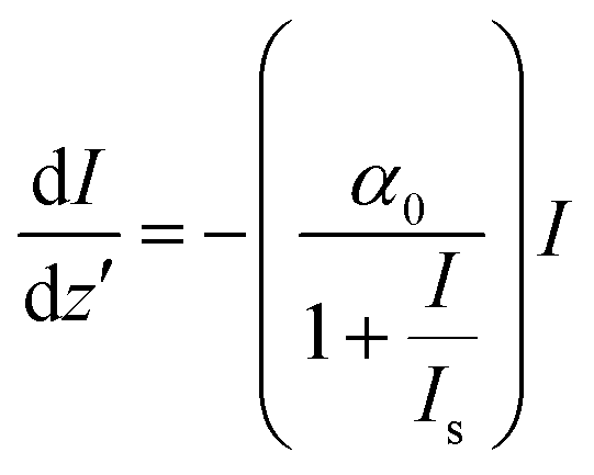 | (2) |
 | ||
| Fig. 7 (a) Normalized transmittance of a pure PEDOT:PSS film as a function of sample position. Experimental data are depicted as circles, while theoretical fits based on eqn (2) are shown as solid lines. (b) Mechanism of saturable absorption. | ||
Estimated values of the nonlinear absorption coefficient (β) and saturation intensity (Is) of PEDOT:PSS and PhC can be found in Table 1. The results are consistent with the previous reports by S Paul et al.42 For a more detailed analysis of saturation effects, Z-scan experiments have been conducted at different peak intensities. The increased transmittance on high light fluences can be explained based on a two-level system, consisting of ground-state and excited state (see Fig. 7(b)). When the absorption cross-section of the excited state is lower than that of its ground state, bleaching of ground-state electrons occurs, leading to saturation of absorption. This occurs because of Pauli's blocking, a phenomenon where the excitation of electrons from the valence band (VB) to the conduction band (CB) is hindered, preventing any further absorption of laser pulses.56
| Sample | Linear transmittance (%) | β ×10−6 (m W−1) | I s × 1012 (W m−2) |
|---|---|---|---|
| PEDOT:PSS | 30 | — | 2.02 |
| PhC | 90 | 1.42 | — |
3.3. Asymmetric light propagation in PhC/PEDOT:PSS multilayer system
We demonstrate that the tunable RSA behavior in PhC and SA behavior in PEDOT:PSS can be used to realize a passive all-optical non-reciprocal device. Such a device is an optical analogous to an electronic pn junction. In an electronic diode, the application of external bias voltage controls the flow of current, whereas in an all-optical diode, the transmission is controlled by axially asymmetric nonlinearity in the system. Since the electromagnetic wave equations obey the time-reversal symmetry, light propagation through a medium follows optical reciprocity. In other words, the transmission through the medium remains unaffected by swapping the detector and source positions.20 However, the asymmetry in the nonlinear absorption behavior can break this symmetry, if the laser intensity is sufficiently high, above a threshold value. In this case, either the SA or RSA nonlinear processes will dominate over the other, contingent upon the laser fluence experienced by each material.Optical non-reciprocity in light transmission, quantified by the non-reciprocity factor (NRF), defines the core metric of optical diode performance. This factor captures the asymmetry in light transmission, reflecting the ratio of forward nonlinear transmittance enhancement (relative to linear transmittance) to reverse nonlinear transmittance reduction (relative to linear transmittance).
Mathematically, NRF is expressed as:20,22
 | (3) |
The schematic illustration of the photonic diode is given in Fig. 8. In forward condition, the laser pulses the first incident on the PEDOT:PSS (see Fig. 8(a)). Due to the saturable absorption process, the output transmittance increases from its linear transmittance and keeps increasing with the intensity of the incoming pulse. This increased intensity then falls on the PhC, causing a decrease in the effective transmission due to the RSA effect. Depending on the coefficients of nonlinear absorption in both materials, the overall impact on transmission will be primarily dominated by either SA or RSA. The SA effect starts to dominate over the RSA effect when intensities are sufficiently greater than the Is value of PEDOT:PSS film. Since the SA term dominates, the net output is the increase in transmission, above the linear transmission of the whole system. This intensity-dependent increased light transmission is referred to as a forward operation.
 | ||
| Fig. 8 The schematic illustration represents the working of an all-optical diode. (a) In the forward-biased configuration, transmitted light shows SA-like behavior, and in (b) the reverse-biased arrangement, it shows RSA-like behavior. The green light in the output of each configuration represents a linear transmitted pulse, and the dark green corresponds to a nonlinearly transmitted light. (c) Schematic illustration of the spectral response of the photonic diode. The low band edge mode (532 nm) and the peak of the stop band (488 nm) are indicated. Enhanced light–matter interaction near the low-energy band edge (532 nm) is attributed to the slow light effect. | ||
The reverse operation condition is characterized by a decrease in the net transmittance as the input intensity increases (see Fig. 8(b)). In this scenario, the laser beam initially interacts with the RSA medium before passing through the SA medium. The RSA effect in the PhC causes attenuation of the input intensity. The saturation effects will take into a considerable change in the output only if the excitation intensity of the SA medium is sufficiently high to induce nonlinearity. Thus, in the reverse direction, the sample exhibits a reduced transmission as increasing the input intensity.
For a detailed explanation of the photonic diode's operating principle, readers are referred to R. Philip et al.16 Briefly, the underlying mechanism is as follows: in the forward condition, the output intensity obtained from eqn (2) is used as the input for eqn (1). Conversely, in the reverse condition, the output intensity obtained from eqn (1) is utilized as the input for eqn (2). A nonreciprocity is created in the output intensity, leading to asymmetric direction-dependent light propagation. However, the parameters in eqn (1) and (2) need to be optimized to get a noticeable change or contrast in the output intensities. Since material parameters like Is and βrsa cannot be adjusted during the fabrication process, the remaining variables to work with are the sample length and linear transmittance of the PEDOT:PSS film.
Fig. 9 validates the practicality of the fabricated device. The normal incidence transmission characteristic of an optical diode working on 20 μJ input energy is shown in Fig. 9(a). The experimentally obtained values of the normalized transmittance of the optical diode in forward and reverse bias configurations are plotted in red and blue triangles, respectively. This device exhibits optical diode characteristics at an intensity above ∼1011 W m−2, and intensities below this display reciprocal transmission. The value is called the onset intensity, where the sample exhibits the transition from linear to nonlinear behavior. Here, the linear transmittance of the PEDOT:PSS film is ∼30%. The intensity of laser pulses varied from 1010 W m−2 to 1012 W m−2, translating the sample through the focus of a 10 cm focal length biconvex lens. The intensity at each point is calculated from the spatial geometry of the focussed beam and transmitted intensity is collected using a pyroelectric detector placed at the far-field. This detector is placed behind a convex lens to capture the laser beam effectively.
 | ||
| Fig. 9 Transmission characteristics of the PEDOT:PSS/PhC optical diode. Light transmission in forward bias (red circle) and reverse bias (black square). Diode transmission plot for (a) 0°, (b) 10°, (c) 20°, and (d) 30°. | ||
The nonreciprocity factor of this device is 12.5 dB, and it is comparable to that of other reported optical diodes based on the SA/RSA cascaded structure. Table 2 summarizes the comparison of different optical diode systems, the laser sources used to characterize them, and the non-reciprocity factor obtained in a specific intensity range. To get a better NRF value, the SA and RSA contrast must be larger. Hence, the large RSA coefficient of the PhC contributes to the better NRF value.
| Diode structure SA/RSA | Laser parameters | Nonreciprocity factor (dB) | Ref. |
|---|---|---|---|
| Ti3C2Tx MXene/C60 | 1064 nm, 7 ns | 4.13 | 20 |
| GeSe/C60 | 1064 nm, 7 ns, 10 ps, and 56 fs | ∼3 | 22 |
| Franckeite/C60 | 1064 nm, 220 ps | ∼2 | 24 |
| Ag NPs/phenothiazine–Ag composite | 532 nm, 7 ns | ∼3 | 17 |
| Boron quantum dots/ReS2 | 515 nm and 1030 nm, 0.394–5.34 ps and 4.45–115 ps | 2.5 | 25 |
| Au/PhC | 532 nm, 7 ns | ∼4.67 | 57 |
| Titanium nitride/hexagonal gold nanolayer | 540 nm, 35 fs | 4.8 | 58 |
| Aluminum-doped zinc oxide/PEA2PbI4 | 1550 nm, 35 fs | 10.1 | 26 |
| Colored glass filter/copper pthalocyanine | 532 nm, 3 ns | — | 16 |
| Graphene/C60 | 532 nm, 5 ns | 4.9 and 6.2 | 3 |
| 2D-tellurium/SnS2 | 457 nm, 532 nm, and 671 nm CW light | — | 21 |
| TiN/C60 | 500 nm, 530 nm, 600 nm, 10–15 ps | 8, 9.5, 5.5 | 59 |
| Graphdiyne/SnS2 | 532 and 671 nm, CW light | — | 23 |
| Sb/C60 | 780 nm and 1560 nm, 100 fs | 5 and 2 | 60 |
| PEDOT:PSS/PhC | 532 nm, 7 ns | ∼12.5 | This work |
The diode operation is sensitive to the angle of laser incidence since the RSA in PhC depends on how well the laser frequency aligns with the photonic band-edge mode of the PhC. As discussed in Section 3.1, the nonlinear absorption properties of the PhC are largely enhanced for normal and near-normal (less than 10°) incidence and significantly reduced at large angles. This tunable nonlinear absorption properties of the system are employed to finely adjust the operations of the diode. The SA response of the PEDOT:PSS film is expected to remain unchanged by small angle variations, as the film is isotropic and homogeneous. The angle-tunable diode actions are shown in Fig. 9(a)–(d). The data are collected for different angles of laser incidence, 0°, 10°, 20° and 30°. The NRF values are 12.5 dB, 8.45 dB, 4.93 dB, and 4.19 dB, respectively. The tunability in NRF values arises from the angle-dependent nonlinear transmission characteristics of the PhC. This feature makes this device a suitable candidate for photonic applications. Compared to other reported photonic diodes, our diode exhibits superior NRF values, while being scalable and easily processable.
4. Conclusion
This work presents an all-polymeric optical diode based on the principle of asymmetric nonlinear absorption in the nonlinear regime. In contrast to earlier diodes employing this principle, this diode architecture offers a simplified fabrication process, exhibits a compact footprint, and eliminates the need for a liquid phase. The realized optical diode consists of a simple structure employing PEDOT:PSS as a saturable absorber medium and a one-dimensional polymeric photonic crystal structure composed of gold–carbon core–shell nanostructures (Au@C NS) as a reverse saturable absorber medium. In this diode, integration of the active medium into a PhC architecture provides a unique avenue for engineering light–matter interactions. Nonlinear optical characterization was conducted employing the Z-scan, utilizing a Q-switched Nd:YAG laser emitting 7 nanosecond pulses at 532 nm. This diode exhibits angular dependence in its light transmission properties. This allows for the control of non-reciprocity by adjusting the incident light angle. For incident angles of 0°, 10°, 20°, and 30°, the NRF values are 12.5 dB, 8.45 dB, 4.93 dB, and 4.19 dB, respectively. This promising combination makes this system a potential candidate for developing compact photonic integrated devices.Data availability statement
The data that support the findings of this study are available within the article and its ESI.†Conflicts of interest
The authors declare no conflict of interest.Acknowledgements
The authors acknowledge Dr Shiju E and Prof. C S Suchand Sandeep for the fruitful discussion. JF and NPP acknowledge the Ministry of Education, Govt of India for financial assistance.References
- Z. Wang and S. Fan, Opt. Lett., 2005, 30, 1989–1991 CrossRef PubMed.
- D. Jalas, A. Petrov, M. Eich, W. Freude, S. Fan, Z. Yu, R. Baets, M. Popović, A. Melloni, J. D. Joannopoulos, M. Vanwolleghem, C. R. Doerr and H. Renner, Nat. Photonics, 2013, 7, 579–582 CrossRef CAS.
- B. Anand, R. Podila, K. Lingam, S. R. Krishnan, S. Siva Sankara Sai, R. Philip and A. M. Rao, Nano Lett., 2013, 13, 5771–5776 CrossRef CAS PubMed.
- P. Yang, X. Xia, H. He, S. Li, X. Han, P. Zhang, G. Li, P. Zhang, J. Xu, Y. Yang and T. Zhang, Phys. Rev. Lett., 2019, 123, 233604 CrossRef CAS PubMed.
- L. Bi, J. Hu, P. Jiang, D. H. Kim, G. F. Dionne, L. C. Kimerling and C. A. Ross, Nat. Photonics, 2011, 5, 758–762 CrossRef CAS.
- F. Ruesink, M. A. Miri, A. Alù and E. Verhagen, Nat. Commun., 2016, 7, 1–8 Search PubMed.
- D. L. Sounas, C. Caloz and A. Alù, Nat. Commun., 2013, 4, 1–7 Search PubMed.
- S. R. Entezar and R. Vatannejad, J. Nonlinear Opt. Phys. Mater., 2016, 25, 1–7 CrossRef.
- K. Jamshidi-Ghaleh and Z. Safari, Int. J. Mod. Phys.: Conf. Ser., 2012, 15, 48–53 CAS.
- M. D. Tocci, M. J. Bloemer, M. Scalora, J. P. Dowling and C. M. Bowden, Appl. Phys. Lett., 1995, 66, 2324–2326 CrossRef CAS.
- C. Y. Wang, C. W. Chen, H. C. Jau, C. C. Li, C. Y. Cheng, C. T. Wang, S. E. Leng, I. C. Khoo and T. H. Lin, Sci. Rep., 2016, 6, 30873 CrossRef CAS PubMed.
- J. Hwang, M. H. Song, B. Park, S. Nishimura, T. Toyooka, J. W. Wu, Y. Takanishi, K. Ishikawa and H. Takezoe, Nat. Mater., 2005, 4, 383–387 CrossRef CAS PubMed.
- M. S. Kang, A. Butsch and P. S. J. Russell, Nat. Photonics, 2011, 5, 549–553 CrossRef CAS.
- L. Fan, J. Wang, L. T. Varghese, H. Shen, B. Niu, Y. Xuan, A. M. Weiner and M. Qi, Science, 2012, 335, 447–450 CrossRef CAS PubMed.
- S. Guddala, Y. Kawaguchi, F. Komissarenko, S. Kiriushechkina, A. Vakulenko, K. Chen, A. Alù, V. M. Menon and A. B. Khanikaev, Nat. Commun., 2021, 12, 3746 CrossRef CAS PubMed.
- R. Philip, M. Anija, C. S. Yelleswarapu and D. V. G. L. N. Rao, Appl. Phys. Lett., 2007, 91, 141118 CrossRef.
- E. Shiju, M. Bharat, N. K. Siji Narendran, D. Narayana Rao and K. Chandrasekharan, Opt. Mater., 2020, 99, 109557 CrossRef CAS.
- L. Wu, X. Yuan, D. Ma, Y. Zhang, W. Huang, Y. Ge, Y. Song, Y. Xiang, J. Li and H. Zhang, Small, 2020, 16, 2002252 CrossRef CAS PubMed.
- B. Sun, Y. Zhang, R. Zhang, H. Yu, G. Zhou, H. Zhang and J. Wang, Adv. Opt. Mater., 2017, 5, 1600937 CrossRef.
- Y. Dong, S. Chertopalov, K. Maleski, B. Anasori, L. Hu, S. Bhattacharya, A. M. Rao, Y. Gogotsi, V. N. Mochalin and R. Podila, Adv. Mater., 2018, 30, 1705714 CrossRef PubMed.
- L. Wu, W. Huang, Y. Wang, J. Zhao, D. Ma, Y. Xiang, J. Li, J. S. Ponraj, S. C. Dhanabalan and H. Zhang, Adv. Funct. Mater., 2019, 29, 1806346 CrossRef.
- J. Tang, F. Zhang, F. Zhou, X. Tang, X. Dai and S. Lu, Nanophotonics, 2020, 9, 2007–2015 CrossRef CAS.
- L. Wu, Y. Dong, J. Zhao, D. Ma, W. Huang, Y. Zhang, Y. Wang, X. Jiang, Y. Xiang, J. Li, Y. Feng, J. Xu and H. Zhang, Adv. Mater., 2019, 31, 1807981 CrossRef PubMed.
- J. Li, L. Du, J. Huang, Y. He, J. Yi, L. Miao, C. Zhao and S. Wen, Nanophotonics, 2021, 10, 927–935 Search PubMed.
- S. Meng, Q. Chen, H. Lin, F. Zhou, Y. Gong, C. Pan and S. Lu, Nanomaterials, 2021, 11, 687 CrossRef CAS PubMed.
- Y. Xu, J. Li, J. Huang, Y. He, X. Liu, L. Zhao, G. Chen and L. Miao, Results Phys., 2023, 52, 106763 CrossRef.
- A. Krasnok, M. Tymchenko and A. Alù, Mater. Today, 2018, 21, 8–21 CrossRef CAS.
- M. Taghinejad and W. Cai, ACS Photonics, 2019, 6, 1082–1093 CrossRef CAS.
- J. Qin, Y.-H. Chen, Z. Zhang, Y. Zhang, R. J. Blaikie, B. Ding and M. Qiu, Phys. Rev. Lett., 2020, 124, 063902 CrossRef CAS PubMed.
- S. Valligatla, A. Chiasera, S. Varas, P. Das, B. N. Shivakiran Bhaktha, A. Łukowiak, F. Scotognella, D. Narayana Rao, R. Ramponi, G. C. Righini and M. Ferrari, Opt. Mater., 2015, 50, 229–233 CrossRef CAS.
- L. Lu, Y. Guo, B. Zhao, H. Wang and Y. Miao, Mater. Today, 2024, 74, 109–120 CrossRef.
- F. C. Krebs, J. Fyenbo and M. Jørgensen, J. Mater. Chem., 2010, 20, 8994–9001 RSC.
- J. H. Burroughes, C. A. Jones and R. H. Friend, Nature, 1988, 335, 137–141 CrossRef.
- F. Charra and J.-M. Nunzi, J. Opt. Soc. Am. B, 1991, 8, 570–577 CrossRef CAS.
- M. Boussoualem, R. C. Y. King, J.-F. Brun, B. Duponchel, M. Ismaili and F. Roussel, J. Appl. Phys., 2010, 108, 113526 CrossRef.
- Q. Hu, X. Yu, H. Liu, J. Qiu, W. Tang, S. Liang, L. Li, M. Du, J. Jia and H. Ye, ACS Photonics, 2023, 10, 3612–3620 CrossRef CAS.
- L. Groenendaal, F. Jonas, D. Freitag, H. Pielartzik and J. R. Reynolds, Adv. Mater., 2000, 12, 481–494 CrossRef CAS.
- C. S. S. Sangeeth, M. Jaiswal and R. Menon, J. Appl. Phys., 2009, 105, 063713 CrossRef.
- X. Fan, W. Nie, H. Tsai, N. Wang, H. Huang, Y. Cheng, R. Wen, L. Ma, F. Yan and Y. Xia, Adv. Sci., 2019, 6, 1900813 CrossRef CAS PubMed.
- Y. Yang, H. Deng and Q. Fu, Mater. Chem. Front., 2020, 4, 3130–3152 RSC.
- K. Sun, S. Zhang, P. Li, Y. Xia, X. Zhang, D. Du, F. H. Isikgor and J. Ouyang, J. Mater. Sci.: Mater. Electron., 2015, 26, 4438–4462 CrossRef CAS.
- S. Paul and K. Balasubramanian, Spectrochim. Acta, Part A, 2021, 245, 118901 CrossRef CAS PubMed.
- Y. Sun, H. Li, R. Hou, M. Diao, Y. Liang, Z. Huang, M. G. Humphrey and C. Zhang, ACS Appl. Mater. Interfaces, 2020, 12, 48982–48990 CrossRef CAS PubMed.
- N. Puthiya Purayil, A. K. Satheesan, S. Edappadikkunnummal and C. Keloth, Opt. Laser Technol., 2023, 159, 109009 CrossRef CAS.
- J. Francis, N. Puthiya Purayil, S. Edappadikkunnummal, C. Keloth and C. S. Suchand Sangeeth, J. Mol. Liq., 2023, 123048 CrossRef CAS.
- T. Hattori, N. Tsurumachi and H. Nakatsuka, J. Opt. Soc. Am. B, 1997, 14, 348–355 CrossRef CAS.
- S. Edappadikkunnummal, N. Puthiya Purayil, J. Francis, A. G. Al-Sehemi, M. Pannipara, R. Thundiparambil Muraleedharan, A. S. Mercy and N. R. Desai, ACS Appl. Polym. Mater., 2023, 5, 5896–5905 CrossRef CAS.
- J. D. Joannopoulos, P. R. Villeneuve and S. Fan, Nature, 1997, 386, 143–149 CrossRef CAS.
- P. Lova, G. Manfredi and D. Comoretto, Adv. Opt. Mater., 2018, 6, 1800730 CrossRef.
- M. Rumi and J. W. Perry, Adv. Opt. Photonics, 2010, 2, 451–518 CrossRef CAS.
- R. T. Tom, A. S. Nair, N. Singh, M. Aslam, C. L. Nagendra, R. Philip, K. Vijayamohanan and T. Pradeep, Langmuir, 2003, 19, 3439–3445 CrossRef CAS.
- R. L. Sutherland, Handbook of Nonlinear Optics, CRC Press, Boca Raton, 2nd edn, 2003 Search PubMed.
- J.-F. Lami, P. Gilliot and C. Hirlimann, Phys. Rev. Lett., 1996, 77, 1632–1635 CrossRef CAS PubMed.
- N. Dong, Y. Li, S. Zhang, N. McEvoy, R. Gatensby, G. S. Duesberg and J. Wang, ACS Photonics, 2018, 5, 1558–1565 CrossRef CAS.
- J. N. Joannopoulos, J. D. Meade and R. D. Winn, Photonic Crystals: Molding the Flow of Light, Princeton Univ. Press, Princeton, 1995 Search PubMed.
- H. Yang, X. Feng, Q. Wang, H. Huang, W. Chen, A. T. S. Wee and W. Ji, Nano Lett., 2011, 11, 2622–2627 CrossRef CAS PubMed.
- N. Puthiya Purayil, V. Kakekochi, U. K. Dalimba and C. Keloth, ACS Appl. Electron. Mater., 2022, 4, 138–148 CrossRef CAS.
- J. Li and J. Huang, Opt. Commun., 2024, 560, 130479 CrossRef CAS.
- J. Huang, Y. He, H. Zhu, Q. Chen, Y. Xu, L. Miao and C. Zhao, Appl. Phys. Lett., 2022, 121, 121102 CrossRef CAS.
- J. Zhang, J. Li, L. Miao and C. Zhao, IEEE Photonics J., 2020, 12, 1–7 Search PubMed.
Footnotes |
| † Electronic supplementary information (ESI) available. See DOI: https://doi.org/10.1039/d4tc02201g |
| ‡ J. F. and N. P. P. contributed equally to this work. |
| § Present address: School of Physics, IISER Thiruvananthapuram, Kerala 695551, India. |
| This journal is © The Royal Society of Chemistry 2024 |