
Introduction of defects in hexagonal boron nitride for vacancy-based 2D memristors†
Haohan
Chen
ab,
Yu
Kang
b,
Dong
Pu
b,
Ming
Tian
c,
Neng
Wan
 c,
Yang
Xu
b,
Bin
Yu
b,
Wenjing
Jie
*a and
Yuda
Zhao
*b
c,
Yang
Xu
b,
Bin
Yu
b,
Wenjing
Jie
*a and
Yuda
Zhao
*b
aCollege of Chemistry and Materials Science, Sichuan Normal University, Chengdu, 610066, China. E-mail: wenjing.jie@sicnu.edu.cn
bSchool of Micro–Nano Electronics, Hangzhou Global Scientific and Technological Innovation Centre, Zhejiang University, 38 Zheda Road, Hangzhou 310027, China. E-mail: yudazhao@zju.edu.cn
cKey Laboratory of MEMS of the Ministry of Education, School of Electronics Science and Engineering, Southeast University, Nanjing 210096, China
First published on 9th February 2023
Abstract
Two-dimensional (2D) materials have become potential resistive switching (RS) layers to prepare emerging non-volatile memristors. The atomically thin thickness and the highly controllable defect density contribute to the construction of ultimately scaled memory cells with stable switching behaviors. Although the conductive bridge random-access memory based on 2D hexagonal boron nitride has been widely studied, the realization of RS completely relying on vacancies in 2D materials has performance superiority. Here, we synthesize carbon-doped h-BN (C-h-BN) with a certain number of defects by controlling the weight percentage of carbon powder in the source. These defects can form a vacancy-based conductive filament under an applied electric field. The memristor displays bipolar non-volatile memory with a low SET voltage of 0.85 V and shows a long retention time of up to 104 s at 120 °C. The response times of the SET and RESET process are less than 80 ns and 240 ns, respectively. The current mapping by conductive atomic force microscopy demonstrates the electric-field-induced current tunneling from defective sites of the C-h-BN flake, revealing the defect-based RS in the C-h-BN memristor. Moreover, C-h-BN with excellent flexibility can be applied to wearable devices, maintaining stable RS performance in a variety of bending environments and after multiple bending cycles. The vacancy-based 2D memristor provides a new strategy for developing ultra-scaled memory units with high controllability.
 Yuda Zhao | Yuda Zhao is an assistant professor at Zhejiang University. He received his Ph.D. from Hong Kong Polytechnic University (supervisor: Prof. Yang Chai). He subsequently engaged in post-doctoral research at the Hong Kong Polytechnic University and the University of Strasbourg (supervisor: Prof. Paolo Samorì). He has been awarded the Marie Skłodowska-Curie Individual Fellowship and Young Elite Scientists Sponsorship Program by the China Association for Science and Technology. His research interests focus on the physical properties of 2D materials, nanoelectronic devices, and applications of 2D devices in the post-Moore era. |
Introduction
2D materials with atomically thin thickness can ultimately downscale the physical dimensions of electronic devices. The distinct physical properties of 2D materials have been adapted to enrich the device functionality. Resistive switching (RS) devices can change the electrical resistance by applying external voltages, exhibiting fast access time, low power storage, non-volatility and high integration density.1,2 RS devices comprising two-dimensional (2D) materials as the switching layer display unique advantages, including tunable switching behavior (threshold switching or resistive switching), controllable neuromorphic properties (potentiation and relaxation), and ultra-low power consumption.3 Compared with the traditional RS layer (metal oxide) in resistive random-access memory (RRAM), 2D hexagonal boron nitride (h-BN) displays a low leakage current in nanometre thickness and it could help reduce the current crosstalk between adjacent elements in crossbar arrays.4,5 The excellent properties of RRAM devices based on 2D materials contribute to their promising applications in information storage and neuromorphic computing.6,7In recent studies, 2D material-based non-volatile memristors have been extensively reported and the use of active metal electrodes leads to the formation of a conductive metal filament in the 2D RS layers.8,9 The shortcomings of this mechanism include the random injection of active metals and uncontrolled damage to the RS layer, resulting in degradation of the retention properties of the device.5,10 Therefore, 2D memristors based on intrinsic defects have attracted a new round of attention. Akinwande et al. prepared the thinnest memristor using a monolayer of chemical vapor deposition (CVD) grown h-BN and successfully demonstrated 2D RRAM using inert metals as both the top and bottom electrodes.11 Lanza et al. prepared CVD grown multilayer h-BN memristors with both top and bottom Au electrodes to study the effects of defects, wrinkles and polymer residues on the electrical properties.4 Han et al. prepared vacancy-based h-BN memristors using transferred Au electrodes to form van der Waals contacts.5 Although these studies have provided a fundamental theory of vacancy-based h-BN, the defect densities in h-BN have not been accurately regulated. We believe that the precise introduction of defects into 2D materials can achieve the reliable formation and fracture of vacancy-based conductive filaments in 2D RRAM.12
As a widely used 2D RS material, h-BN can be prepared via CVD, liquid exfoliation (LE) and mechanical exfoliation (ME) methods.13–15 A large number of vacancies can be created during the CVD and LE preparation process accompanied by grain boundaries, wrinkles and contaminations. In contrast, the mechanically exfoliated flakes from high-quality crystals have very few defects.4 A method to controllably create vacancies should be well designed and then the vacancy-based 2D RRAM can be systematically explored.
In our work, h-BN crystals have been grown at atmospheric pressure and high temperature (APHT) using a metal alloy solvent. The vacancy concentration in the h-BN crystals can be effectively tuned by adding carbon powder to the sources. Extensive material characterization methods, including high-resolution transmission electron microscopy (HRTEM), X-ray photoelectron spectroscopy (XPS), energy-dispersive X-ray spectroscopy (EDS), photoluminescence (PL), and conductive atomic force microscopy (C-AFM), have been used to demonstrate the presence of boron vacancies in carbon-doped h-BN (C-h-BN). The vacancy-based RRAM devices consist of C-h-BN as the RS layer and Au as both the top and bottom electrodes. The electrical characterization results show non-volatile resistive switching behavior, a high ON/OFF ratio, a fast response time, excellent retention at 120 °C, and reliable endurance. Several groups of the control experiment and the conductive atomic force microscopy characterization demonstrate that the switching is due to the migration of vacancies in the C-h-BN layer. The devices on flexible substrates also exhibit high optical transmittance, good bending and cycling stability. The vacancy-based RRAM devices can avoid the massive damage to the RS layer from the metal ions.5,16 Our work shows the potential to accurately control the vacancy concentration in h-BN and prepare vacancy-based RRAM devices with a long retention time and high device stability.
Experimental methods
Material synthesis
The schematic diagram of the growth process of C-h-BN at APHT is shown in Fig. 1a. Briefly speaking, h-BN powder was mixed with the Ni–Cr alloy in a cylindrical crucible. The carbon powder was added to tune the vacancy concentration. The weight ratio of the alloy, h-BN powder and carbon powder is 100![[thin space (1/6-em)]](https://www.rsc.org/images/entities/char_2009.gif) :10:0.6.
:10:0.6.
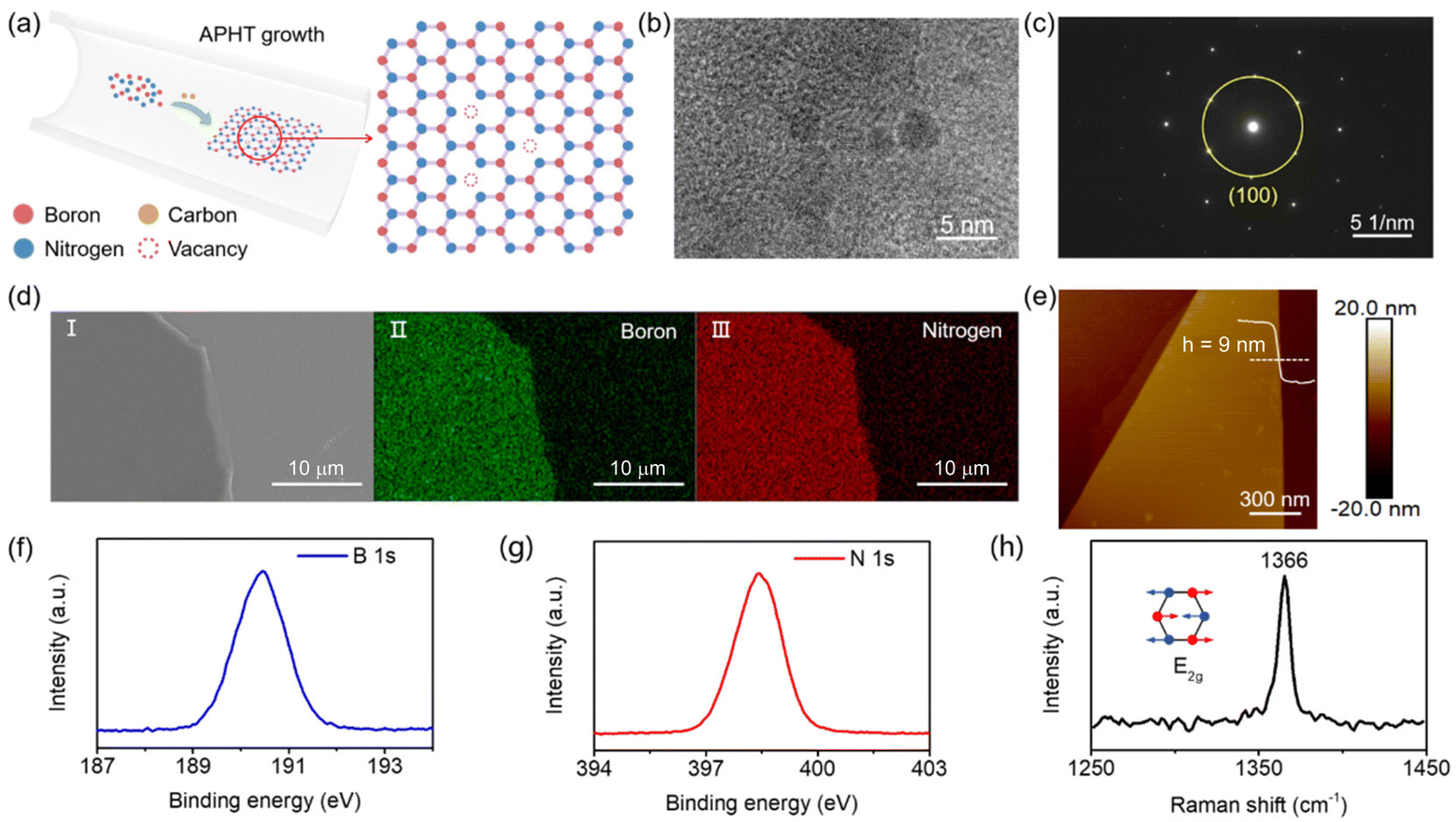 | ||
| Fig. 1 Characterization of the synthesized carbon-doped hexagonal boron nitride (C-h-BN) samples. (a) Schematic diagram of the growth processes. (b) High-resolution transmission electron microscopy (HRTEM) image of the C-h-BN flake. (c) The selected-area electron diffraction pattern of the C-h-BN flake. (d) Scanning electron microscopy image (I) of the C-h-BN flake. Elemental mapping image of B (II) and N (III) of the exfoliated h-BN flake in energy-dispersive X-ray spectroscopy. (e) Atomic force microscopy (AFM) image of the exfoliated h-BN flake. The line profile shows the thickness of the flake, which is 9 nm. X-ray photoelectron spectroscopy (XPS) of (f) B 1s and (g) N 1s. (h) Raman spectrum of the exfoliated C-h-BN flake. | ||
Device preparation
The memristor devices were prepared by the deposition of the bottom Au electrode, followed by the transfer of the exfoliated C-h-BN nanosheets, and finally the deposition of the top Au electrode. Au electrodes display a crossbar array with a width of 4 μm and a spacing of 4 μm. To preserve the high-quality interface between the metal and C-h-BN, a dry transfer method was used to place the few-layer C-h-BN flakes on the metal electrodes.Characterization and measurements
The HRTEM (Tecnai G2 F20 S-TWIN) was used to observe the crystal structure of the C-h-BN nanosheets. Scanning electron microscopy (SEM) (Zeiss Sigma 300) equipped with an EDS was used to characterize the surface morphology and chemical compositions of the C-h-BN nanosheets. Atomic force microscopy (AFM) (Bruker Dimension ICON) was employed to determine the thickness of the exfoliated nanosheets. C-AFM (Oxford MFP-3D Infinity) was used to perform the tunneling current mapping. XPS (Thermo Scientific ESCALAB 250Xi) was used to investigate the elemental composition of the h-BN nanosheets. Raman spectroscopy and PL characterization were performed at room temperature using a Renishaw inVia spectrometer with a confocal microscope (532 nm laser source). The crystal structure was characterized by X-ray diffraction analysis (XRD) (Haoyuan, DX-2700A). Keithley 2450 and Keithley 4200A-SCS parameter analyzers were used to characterize the electrical RS behaviors.Results and discussion
The existence of vacancy in C-h-BN flakes is a prerequisite to realize a vacancy-based RRAM device. The HRTEM image of C-h-BN is shown in Fig. 1b. Several small domains with apparent grain boundaries can be observed.17–19 In contrast, the HRTEM image of the commercial high-quality h-BN flakes displays a perfect lattice structure as shown in Fig. S1.† After careful statistical analysis, the single-crystalline domain in C-h-BN is dominant, leading to a clear dot pattern in the selected-area electron diffraction (SAED) image (Fig. 1c).20,21 These results prove that the as-grown C-h-BN flake preserves the hexagonal crystal structure and contains more vacancies compared to high-quality commercial h-BN. The carbon doping introduces atomic defects in the crystal structures and induces the defect level in the band structure of h-BN. The carrier recombination from defect levels generates the photon emission. A single photon emission peak in the PL spectra of C-h-BN is located at 582 nm, as shown in Fig. S2,† indicating the existence of defect levels.22 With an increase in carbon doping density, the color of the h-BN crystals becomes deeper yellow (Fig. S2†), further confirming the introduction of carbon during the growth process. Fig. 1d shows the SEM image of the exfoliated C-h-BN nanosheets with smooth morphology. The elemental mapping by EDS indicates the uniform elemental distribution of B and N (Fig. 1d).23 The atomic ratio of B and N in C-h-BN (Fig. S3†) is 0.91:1, while the ratio is 0.94:1 in high-quality h-BN. The semi-quantitative analysis of the EDS element ratio shows that the density of the B vacancy increases in C-h-BN. In the vacancy-based RRAM devices, the thickness of the C-h-BN flake is a crucial parameter. In our work, the thickness is about 9 nm from the AFM height image (Fig. 1e), which is an estimated layer number of 27.24,25 As shown in Fig. 1f–h, XPS and Raman spectroscopy were also used to characterize the chemical composition and the phonon vibration properties of C-h-BN flake crystals. The two distinctive peaks located at 190.45 eV and 398.4 eV correspond to B 1s and N 1s, respectively.5,26,27 We assume that the B/N ratio in high-quality h-BN is 1:1, and the B/N ratio in C-h-BN is calculated to be 0.96:1. This indicates that the C-h-BN sample has a higher density of B vacancies than high-quality h-BN. We cannot observe C–N or C–B bonding in the XPS spectra, which is consistent with a previous report.28 The Raman peak at 1366 cm−1 belongs to the E2g phonon vibration mode.5,26,29 Fig. S4† shows the XRD pattern of the C-h-BN crystals. The main peak reflection is positioned at 2θ of ∼26.6°, which is the (002) plane of the h-BN structure.30 The high-crystalline lattice with a certain number of boron vacancies in C-h-BN is very useful to build vacancy-based RRAM devices.
The schematic diagram in Fig. 2a illustrates the device structure of the vacancy-based RRAM. The C-h-BN nanosheet is sandwiched between the Au top electrode and the Au bottom electrode. The crossbar array of RRAM consists of 5 × 3 devices and the corresponding optical image of our prepared devices is shown in Fig. 2b. The area of the h-BN flake is about 220 μm2. In order to prevent Joule heating damage to the memristor, the compliance current (Icc) in the electroforming process was set to 10−4 A.31,32 A forming voltage of 4.2 V was required to activate the device (Fig. S5†). In the following switching cycles, non-volatile bipolar RS behaviors can be observed. Fig. 2c shows a typical current–voltage (I–V) curve with the current on a logarithmic scale. The Au/C-h-BN/Au memristor is initially in the high resistance state (HRS). When a voltage of ∼1.1 V is applied, the current increases rapidly and the device is switched from a HRS to a low resistance state (LRS), which is defined as the SET process. The LRS can be maintained during the subsequent positive voltage scanning. When the voltage is decreased to −0.5 V, the device is switched back to the HRS, suggesting the RESET process. The non-volatile RS behavior displays an ON/OFF current ratio of ∼105.
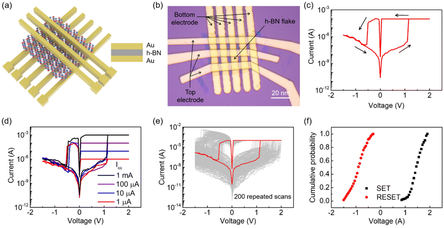 | ||
| Fig. 2 Resistive switching performance of the Au/C-h-BN/Au memristor. (a) Schematic diagram of the device structure (Au/C-h-BN/Au) based on the multilayer C-h-BN flakes. The crossbar array consists of 5 × 3 memory cells. (b) Optical image of Au/C-h-BN/Au memristors in the 5 × 3 crossbar array. (c) Typical non-volatile bipolar I–V curves of the devices. (d) I–V curves with different compliance current (Icc). (e) 200 cycles of I–V scans on the same device. The red line denotes the representative I–V curve. (f) Cumulative probability of the SET and RESET voltages in the 200 repeated scans. | ||
To further understand the RS behaviors of the memristor, the current under positive voltage is re-plotted using double-logarithmic coordinates, as shown in Fig. S6.† During the SET process, the curve can be divided into three regions according to I ≈ Va: an ohmic region (a ≈ 1), a Child's law region (a ≈ 2) and a region where a > 2. This RS behavior follows the space charge limited current (SCLC) injection.33,34 It means that conductive filaments (CFs) are formed between the top and bottom Au electrodes. When the Icc is adjusted between 1 mA and 1 μA, the device can retain the non-volatile RS behavior (Fig. 2d) and the SET voltage remains constant independent of the Icc. This demonstrates that the CFs in the RRAM device are robust and stable. The conductive path can be destroyed and rebuilt in the same region in different switching cycles.
To characterize the cycle-to-cycle variation of our RRAM devices, up to 200 RS scans were performed and the I–V curves were plotted as shown in Fig. 2e. The device can maintain the bipolar non-volatile RS behavior for all the switching cycles. The cumulative probabilities of the SET and RESET voltages are shown in Fig. 2f. Despite the SET and RESET voltages showing slight fluctuations, the memristor still demonstrates typical bipolar RS behaviors with the SET voltages ranging from 0.85 V to 1.95 V and the RESET voltages ranging from −0.3 V to −1.5 V. It is worth noting that the SET voltage can be as low as 0.85 V. In comparison with multilayer h-BN memristors in the reported works, this relatively low SET voltage is helpful to reduce the power consumption of RRAM devices.4,5,9,35–39 As shown in Fig. S7,† 50 crossbar arrays were prepared in our work and the I–V curves of approximately 300 devices were characterized. Almost all the devices show similar non-volatile resistive switching behaviors. The statistical distribution of the SET/RESET voltage of 300 devices displays slight fluctuations and the variation of the SET/RESET voltage is within 1 V. These results demonstrate that our devices have good reproducibility and uniformity. The temperature-dependent retention properties have been characterized at 25 °C, 70 °C and 120 °C. Fig. 3a shows that the memristor can correctly store the information for over 104 s at all temperatures. With an increase in temperature, the high resistance state displays obvious fluctuations, but the device still preserves a resistive ratio of more than 105. We further characterize the resistance of the memristor in the LRS and HRS with the temperature ranging from 250 K to 350 K in the cryogenic probe station. Fig. 3b shows that the resistance in the HRS decreases with an increase in temperature, while the temperature dependency of the LRS is very weak. The LRS resistance slightly decreases with the increasing temperature, which is different from the Ohmic conduction mechanism. Therefore, we believe that the mechanism of our h-BN RRAM is vacancy conduction.40
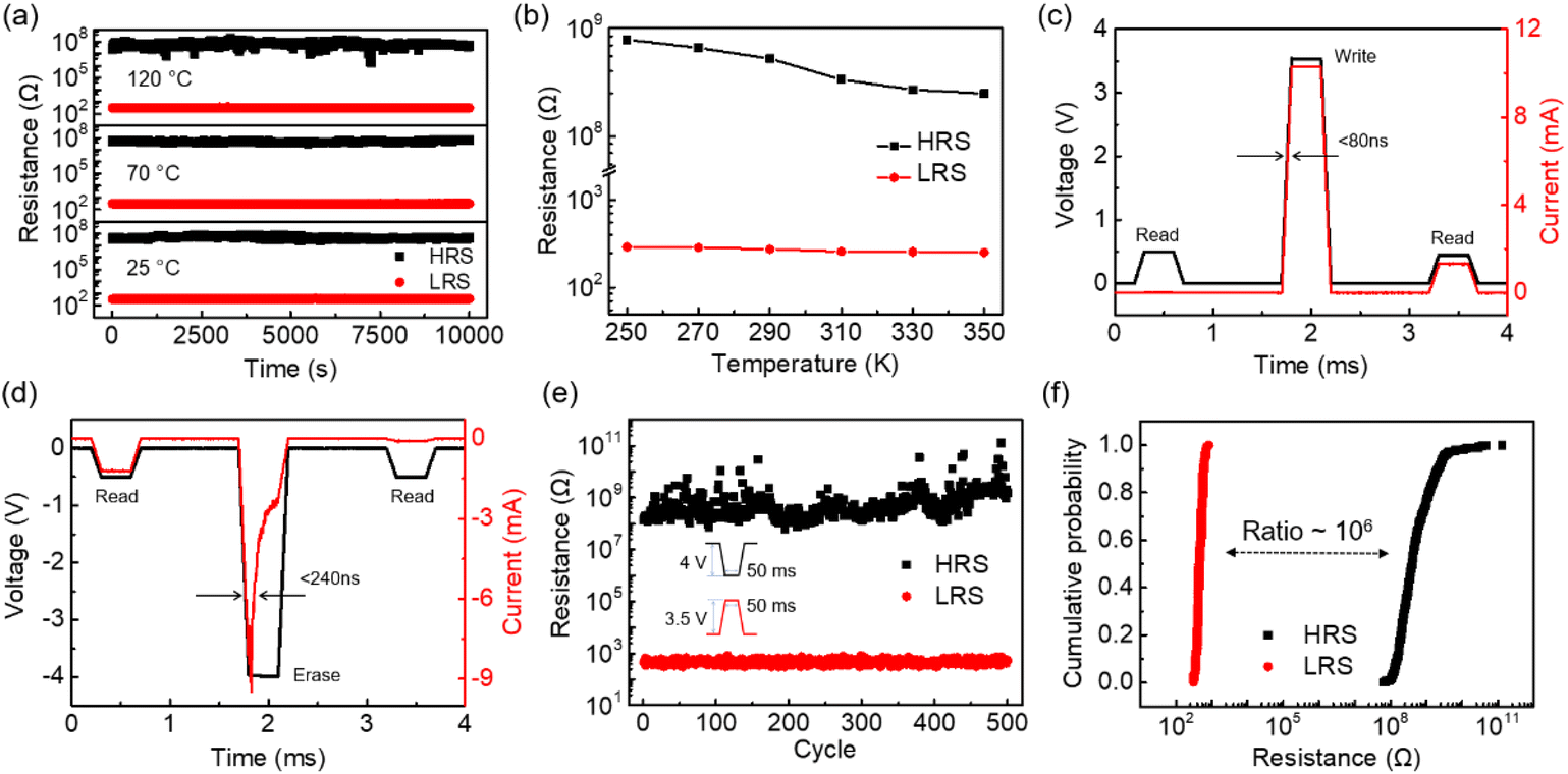 | ||
| Fig. 3 (a) Retention performance of the memristor at 25 °C, 70 °C, and 120 °C. (b) The plot of resistances at HRS and LRS with the temperature. (c) The time-dependent current response of the C-h-BN memristor under pulsed write and read voltages. (d) The time-dependent current response of the C-h-BN memristor under pulsed erase and read voltages. (e) Endurance performance of the memristor. (f) Cumulative probability of the resistance at HRS and LRS. | ||
Beyond DC characterization, the SET/RESET process can be achieved by pulse voltages in C-h-BN memristors. In our C-h-BN RRAM device (Fig. 3c and d), a pulse voltage of 3.5 V with a width of 300 μs is applied to the device. A fast SET process has been observed and the response time is smaller than 80 ns. After the SET process, the current dramatically increases under a read voltage of 0.5 V, displaying a transition from a high resistance state to a low resistance state. A pulse voltage of −4 V with a width of 300 μs is used to conduct the erase operation. The response time of the RESET process is longer than that of the SET process, which is <240 ns. After the erase operation, a high resistance state is observed under a reading voltage of −0.5 V.41,42 The endurance properties of the C-h-BN RRAM devices were characterized under 500 cycles of pulse voltages (Fig. 3e). No obvious degradation can be observed in the 500 cycles of switching. Based on statistical analysis of the endurance curves, the cumulative probabilities of the LRS and HRS were plotted as shown in Fig. 3f. The resistance distribution in the LRS is relatively narrow compared with that in the HRS and the ON/OFF ratio between the LRS and HRS is as high as 106. The relatively large variation of the HRS is perhaps due to the random rupture of the CFs by the large voltage pulse.
To explore the RS mechanism of the C-h-BN RRAM device, several groups of the control experiment were performed. A commercial high-quality h-BN with a nearly perfect crystal lattice was used as the RS layer. The forming process cannot be observed even when the voltage is increased to 30 V (Fig. S8†). This demonstrates that the RS in C-h-BN RRAM is related to the boron vacancies. Then the inert Au top electrode is replaced with an active Ag electrode in C-h-BN RRAM and the SET voltage can be reduced to 0.5 V. However, the cycle-to-cycle I–V curve is extremely unstable and the device exhibits poor durability as shown in Fig. S9.† This is because the formation and rupture of the Ag conductive bridge in the RS layer are random and uncontrollable. Ag CFs will be accumulated in the resistance layer, leading to the short circuit of the device. We also observe that the RESET process of the C-h-BN RRAM device with both the top and bottom Au electrodes can occur under the positive voltage scan (Fig. S10†) due to the rupture of CFs owing to Joule heating. These results demonstrate that the CFs in C-h-BN RRAM with inert electrodes are attributed to the vacancies and defects in the C-h-BN layer. Based on our material characterization results, we infer that the boron vacancies have a high possibility of forming the CFs.43
C-AFM can be used to measure the current mapping of C-h-BN and commercial high-quality h-BN.9,44,45 Two kinds of h-BN flakes are placed on the Au substrate and the Pt probe tip is directly brought into contact with the h-BN surface to build a Pt/h-BN/Au device. The tapping mode AFM images of two kinds of h-BN flakes are shown in Fig. S11,† displaying the same flake thickness. As shown in Fig. 4a, a voltage was applied to the Pt probe and the bottom Au substrate was grounded. The scanning range is 2 μm × 2 μm (∼4 μm2) in the C-AFM measurement. As the electroforming process has not been performed on two kinds of h-BN flakes, the device is in the HRS. In the commercial h-BN device, a tunneling current in the C-AFM image cannot be detected when the applied voltage is increased to as large as 6 V to the probe, indicating a low defect density in the crystal structure of the commercial h-BN device. In the C-h-BN device, a tunneling current on the order of nA can be detected by applying a 0.01 V voltage to the Pt tip. This suggests that C-h-BN has intrinsic defects or vacancies. At these defective sites, the vacancies can be accumulated under an electric field and finally contribute to the CFs.46 A schematic diagram in Fig. 4d is summarized to illustrate the RS process. The C-h-BN RS layer contains a certain number of boron vacancies. When a large positive voltage is applied to the top electrode, a large number of boron vacancies near the top electrode can drift under the vertical electric field.45 When these boron vacancies reach the top electrode, they will accumulate at the top electrode, which represents the starting point of the formation of the CFs. When the boron vacancies gathered at the top electrode are fully connected to the bottom electrodes, the RRAM completes the electroforming process. During the RESET process, when a negative voltage is applied at the bottom electrode, the electric field turns over. The narrowest region near the bottom electrode is the weakest point in the CFs. The reverse migration of boron vacancies and the excessive Joule heating will induce the local rupture of the CFs. During the SET process, the positive voltage induces the reconnection of boron vacancies around the narrowest region of the CFs. Therefore, in the RS process, the rupture and formation of the filament are always located at the narrowest part, corresponding to the RESET and SET processes, respectively.47
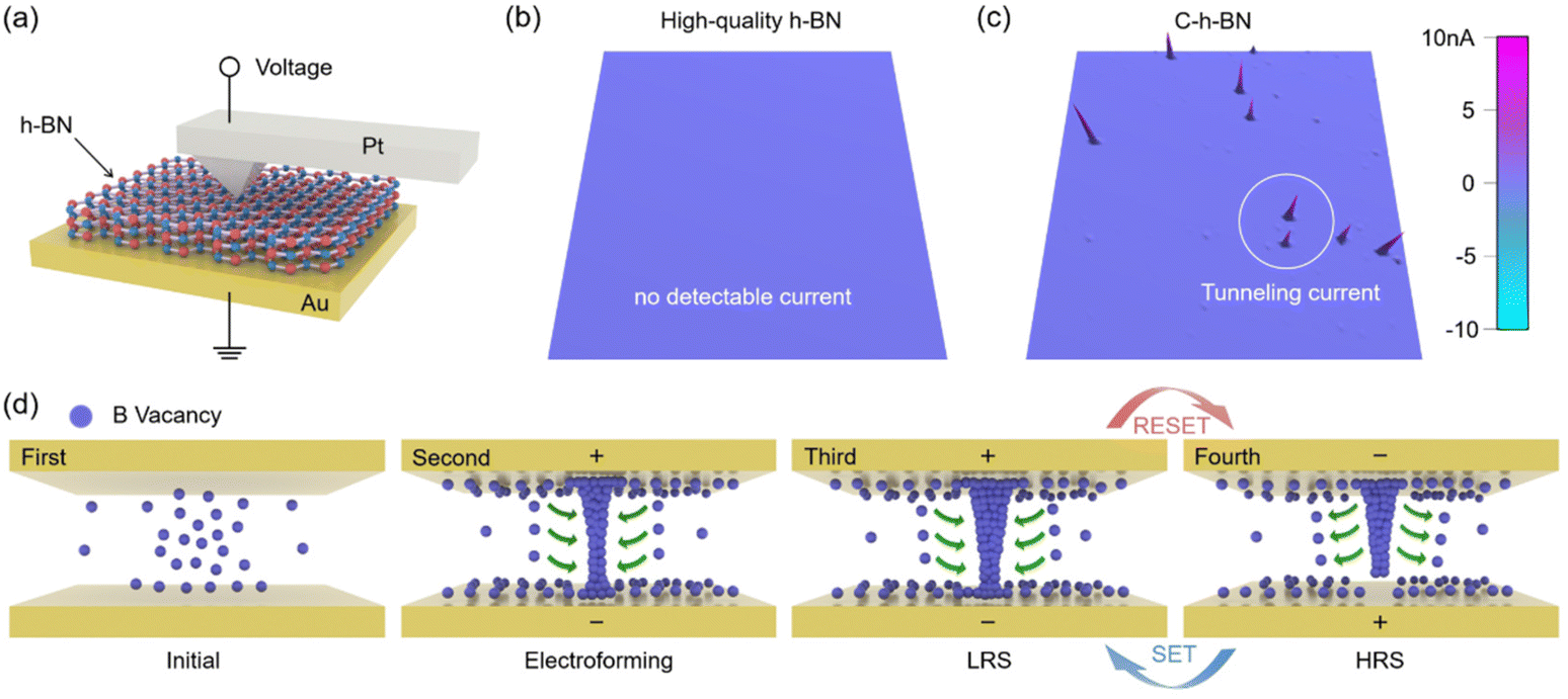 | ||
| Fig. 4 Physical mechanism of the C-h-BN-based memristors. (a) Schematic diagram of the conductive atomic force microscope (C-AFM) experiments. (b) Current mapping image of the Pt/h-BN/Au cell with high-quality h-BN flakes. (c) Current mapping image of the Pt/C-h-BN/Au cell with the as-prepared C-h-BN flake. (d) Schematic diagram of the resistive switching process. It includes the initial state, electroforming process, LRS after the SET process and HRS after the RESET process, respectively. | ||
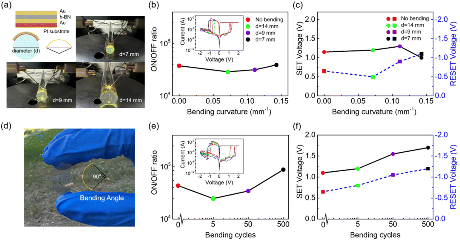
As a 2D material, h-BN has good ductility and a high bending resistance.48,49 The schematic diagram in Fig. 5a is designed to measure the performance of the flexible C-h-BN RRAM devices. The memristor with a Au/C-h-BN/Au structure was prepared on the polyimide (PI) substrate using the same preparation procedure as that on the SiO2/Si substrate. The prepared devices were attached on the glass rods with diameters of 7, 9, and 14 mm, representing different bending curvatures. The inset of Fig. 5b shows the I–V RS curves. The ON/OFF ratio of the device under three bending conditions displays small variations. The LRS and HRS of C-h-BN RRAM can be well recognized under different bending curvatures. The corresponding SET voltage and RESET voltage are close to the pristine one, as shown in Fig. 5c. These results suggest that the bending curvatures from 0 mm−1 to 0.14 mm−1 cannot affect the basic performance of the C-h-BN RRAM. The device has the potential to work stably in the bending environment for flexible applications. Polyethylene terephthalate (PET) substrate can be also used as the substrate and the prepared sample in Fig. 5d shows high transparency and high flexibility. A total number of 500 bending cycles have been performed with a bending angle of 90° (Fig. 5d). The inset of Fig. 5e shows the I–V RS curves. The ON/OFF ratio of the C-h-BN RRAM after 5, 50 and 500 cycles of bending is relatively stable at about 105. The SET and RESET voltages increase slightly after 500 cycles of bending. We infer that the bending process unavoidably affects the CFs in the RS layer and results in the movement of boron vacancies.
 | ||
| Fig. 5 Resistive switching performance of the Au/C-h-BN/Au memristor on flexible substrates. (a) Schematic diagram and optical images of flexible memristor devices with different bending curvatures. (b) ON/OFF current ratio under different bending curvatures. The inset shows the I–V curves at under different bending curvatures. (c) The SET and RESET voltages under different bending conditions. (d) Photograph of the transparent and flexible memristor device with a bending angle of 90°. (e) An ON/OFF current ratio after different bending cycles. (f) The SET and RESET voltages after different bending cycles. | ||
Conclusions
We successfully synthesized C-h-BN flakes with a controllable density of boron vacancies. Several small domains of C-h-BN with a certain number of defects were observed using HRTEM. The EDS elemental analysis confirmed the existence of boron vacancies. The memristor based on C-h-BN displays the robust bipolar non-volatile RS, a lower SET voltage of 0.85 V and a RESET voltage of −0.3 V, a high ON/OFF current ratio of over 105, stable operation cycles and repeatability, a long retention time of 104 s at 120 °C, a fast pulse response of less than 240 ns, and an endurance of 500 pulse switching cycles. Comparing the I–V RS performance of C-h-BN with commercial high-quality h-BN based memristor devices, the formation of a conductive metal bridge can be excluded and the current mapping by C-AFM mode further experimentally demonstrates the crucial role of defects in RS of C-h-BN memristors. Furthermore, the C-h-BN memristor on PI and PET flexible substrates displayed stable RS behavior under the maximum bending curvature of 0.14 mm−1 and after 500 cycles of bending experiments. In this work, the carbon doping during the APHT growth process is used to accurately introduce the vacancy in h-BN crystals to achieve stable RS behavior and excellent RRAM uniformity in device arrays. In addition, our devices exhibit excellent thermal stability and mechanical flexibility, which are also of great advantage in practical applications. It is desirable to explore the use of the CVD method to grow wafer-scale h-BN thin films with controlled vacancy density for building large-scale vacancy-based h-BN memristor arrays. Our results demonstrate that the introduction of vacancies in h-BN can produce stable RS behavior completely based on the vacancy filament and promote the practical applications of 2D memristors in large-scale electronic devices for wearable applications.Author contributions
Haohan Chen and Yu Kang contributed equally to this work. Yuda Zhao, Wenjing Jie, Haohan Chen and Yu Kang conceived and designed the experiments. Haohan Chen and Yu Kang prepared and tested the devices. Haohan Chen characterized the materials. Ming Tian synthesized the C-h-BN crystals and helped with XRD characterization under the supervision of Neng Wan. Dong Pu helped with C-AFM characterization. Yang Xu, Bin Yu, Wenjing Jie and Yuda Zhao edited the manuscript.Conflicts of interest
There are no conflicts to declare.Acknowledgements
We thank the ZJU Micro–Nano Fabrication Center and ZJU–Hangzhou International Innovation Center for the support. The project was primarily supported by the National Natural Science Foundation of China (62090030, 62090034, 62104214, 61974097, 52233014, and 62261160574); the Young Elite Scientists Sponsorship Program by the CAST (2021QNRC001); the Opening Project of Key Laboratory of Optoelectronic Chemical Materials and Devices of Ministry of Education, Jianghan University (No. JDGD–202202); and the National Natural Science Foundation of Sichuan (No. 22NSFSC1257) and Kun–Peng Program of Zhejiang Province.References
- G. R. Bhimanapati, Z. Lin, V. Meunier, Y. Jung, J. Cha, S. Das, D. Xiao, Y. Son, M. S. Strano and V. R. Cooper, ACS Nano, 2015, 9, 11509–11539 CrossRef CAS PubMed.
- X. Duan, C. Wang, A. Pan, R. Yu and X. Duan, Chem. Soc. Rev., 2015, 44, 8859–8876 RSC.
- M. Lanza, F. Hui, C. Wen and A. C. Ferrari, Adv. Mater., 2022, 2205402 Search PubMed.
- Y. Shen, W. Zheng, K. Zhu, Y. Xiao, C. Wen, Y. Liu, X. Jing and M. Lanza, Adv. Mater., 2021, 33, 2103656 CrossRef CAS PubMed.
- J. Y. Mao, S. Wu, G. Ding, Z. P. Wang, F. S. Qian, J. Q. Yang, Y. Zhou and S. T. Han, Small, 2022, 18, 2106253 CrossRef CAS PubMed.
- G. Cao, P. Meng, J. Chen, H. Liu, R. Bian, C. Zhu, F. Liu and Z. Liu, Adv. Funct. Mater., 2021, 31, 2005443 CrossRef CAS.
- J. Tang, C. He, J. Tang, K. Yue, Q. Zhang, Y. Liu, Q. Wang, S. Wang, N. Li and C. Shen, Adv. Funct. Mater., 2021, 31, 2011083 CrossRef CAS.
- H. Zhao, Z. Dong, H. Tian, D. DiMarzi, M. G. Han, L. Zhang, X. Yan, F. Liu, L. Shen and S. J. Han, Adv. Mater., 2017, 29, 1703232 CrossRef PubMed.
- Y. Shi, X. Liang, B. Yuan, V. Chen, H. Li, F. Hui, Z. Yu, F. Yuan, E. Pop and H.-S. P. Wong, Nat. Electron., 2018, 1, 458–465 CrossRef.
- Y.-R. Jeon, Y. Abbas, A. S. Sokolov, S. Kim, B. Ku and C. Choi, ACS Appl. Mater. Interfaces, 2019, 11, 23329–23336 CrossRef CAS PubMed.
- X. Wu, R. Ge, P. A. Chen, H. Chou, Z. Zhang, Y. Zhang, S. Banerjee, M. H. Chiang, J. C. Lee and D. Akinwande, Adv. Mater., 2019, 31, 1806790 CrossRef PubMed.
- F. Ducry, D. Waldhoer, T. Knobloch, M. Csontos, N. Jimenez Olalla, J. Leuthold, T. Grasser and M. Luisier, npj 2D Mater. Appl., 2022, 6, 1–10 CrossRef.
- N. Guo, J. Wei, L. Fan, Y. Jia, D. Liang, H. Zhu, K. Wang and D. Wu, Nanotechnology, 2012, 23, 415605 CrossRef PubMed.
- C. Huo, Z. Yan, X. Song and H. Zeng, Sci. Bull., 2015, 60, 1994–2008 CrossRef CAS.
- A. Pierret, J. Loayza, B. Berini, A. Betz, B. Plaçais, F. Ducastelle, J. Barjon and A. Loiseau, Phys. Rev. B: Condens. Matter Mater. Phys., 2014, 89, 035414 CrossRef.
- C. Pan, Y. Ji, N. Xiao, F. Hui, K. Tang, Y. Guo, X. Xie, F. M. Puglisi, L. Larcher and E. Miranda, Adv. Funct. Mater., 2017, 27, 1604811 CrossRef.
- A. Zavabeti, A. Jannat, L. Zhong, A. A. Haidry, Z. Yao and J. Z. Ou, Nano-Micro Lett., 2020, 12, 1–34 CrossRef PubMed.
- P. Liu, T. Luo, J. Xing, H. Xu, H. Hao, H. Liu and J. Dong, Nanoscale Res. Lett., 2017, 12, 1–10 CrossRef CAS PubMed.
- Q. Wu, J.-H. Park, S. Park, S. J. Jung, H. Suh, N. Park, W. Wongwiriyapan, S. Lee, Y. H. Lee and Y. J. Song, Sci. Rep., 2015, 5, 1–8 Search PubMed.
- Y. Wang, H. Liu, P. Liu, W. Lu, J. Cui, X. Chen and M. Lu, J. Alloys Compd., 2022, 909, 164775 CrossRef CAS.
- X. Chen, H. Yang, B. Wu, L. Wang, Q. Fu and Y. Liu, Adv. Mater., 2019, 31, 1805582 CrossRef PubMed.
- J. Zhou, H. Li, M. Tian, A. Chen, L. Chen, D. Pu, J. Hu, J. Cao, L. Li and X. Xu, ACS Appl. Mater. Interfaces, 2022, 14, 35917–35926 CrossRef CAS PubMed.
- L. Lin, T. Liu, Y. Zhang, R. Sun, W. Zeng and Z. Wang, Ceram. Int., 2016, 42, 971–975 CrossRef CAS.
- K. Kinoshita, R. Moriya, M. Onodera, Y. Wakafuji, S. Masubuchi, K. Watanabe, T. Taniguchi and T. Machida, npj 2D Mater. Appl., 2019, 3, 1–8 CrossRef.
- C. Elias, P. Valvin, T. Pelini, A. Summerfield, C. Mellor, T. Cheng, L. Eaves, C. Foxon, P. Beton and S. Novikov, Nat. Commun., 2019, 10, 1–7 CrossRef CAS PubMed.
- H. Jeong, J. Kim, D. Y. Kim, J. Kim, S. Moon, O. F. Ngome Okello, S. Lee, H. Hwang, S.-Y. Choi and J. K. Kim, ACS Appl. Mater. Interfaces, 2020, 12, 46288–46295 CrossRef CAS PubMed.
- A. Alzahrani, M. Kalutara Koralalage, J. Jasinski and G. Sumanasekera, Electron. Mater. Lett., 2022, 18, 313–320 CrossRef CAS.
- S. Ngamprapawat, T. Nishimura, K. Watanabe, T. Taniguchi and K. Nagashio, ACS Appl. Mater. Interfaces, 2022, 14, 25731–25740 CrossRef CAS PubMed.
- T. Sun, J. Tu, Z. Zhou, R. Sun, X. Zhang, H. Li, Z. Xu, Y. Peng, X. Liu and P. Wangyang, Cell Rep. Phys. Sci., 2022, 3, 100939 CrossRef CAS.
- A. Kumar, G. Malik, S. Sharma, R. Chandra and R. S. Mulik, Ceram. Int., 2021, 47, 30985–30992 CrossRef CAS.
- K. Liao, P. Lei, M. Tu, S. Luo, T. Jiang, W. Jie and J. Hao, ACS Appl. Mater. Interfaces, 2021, 13, 32606–32623 CrossRef CAS PubMed.
- N. K. Upadhyay, W. Sun, P. Lin, S. Joshi, R. Midya, X. Zhang, Z. Wang, H. Jiang, J. H. Yoon and M. Rao, Adv. Electron. Mater., 2020, 6, 1901411 CrossRef CAS.
- Y. Chen, Y. Wang, Y. Luo, X. Liu, Y. Wang, F. Gao, J. Xu, E. Hu, S. Samanta and X. Wan, IEEE Electron Device Lett., 2019, 40, 1686–1689 CAS.
- H.-T. Lin, Z. Pei and Y.-J. Chan, IEEE Electron Device Lett., 2007, 28, 569–571 CAS.
- C. Pan, E. Miranda, M. A. Villena, N. Xiao, X. Jing, X. Xie, T. Wu, F. Hui, Y. Shi and M. Lanza, 2D Mater., 2017, 4, 025099 CrossRef.
- H. Park, M. A. Mastro, M. J. Tadjer and J. Kim, Adv. Electron. Mater., 2019, 5, 1900333 CrossRef CAS.
- W. Lin, P. Zhuang, D. Akinwande, X.-A. Zhang and W. Cai, Appl. Phys. Lett., 2019, 115, 073101 CrossRef.
- K. Zhu, X. Liang, B. Yuan, M. A. Villena, C. Wen, T. Wang, S. Chen, F. Hui, Y. Shi and M. Lanza, ACS Appl. Mater. Interfaces, 2019, 11, 37999–38005 CrossRef CAS PubMed.
- S. Chen, M. R. Mahmoodi, Y. Shi, C. Mahata, B. Yuan, X. Liang, C. Wen, F. Hui, D. Akinwande and D. B. Strukov, Nat. Electron., 2020, 3, 638–645 CrossRef CAS.
- Z. Liu, P. Cheng, Y. Li, R. Kang, Z. Zhang, Z. Zuo and J. Zhao, ACS Appl. Mater. Interfaces, 2021, 13, 58885–58897 CrossRef CAS PubMed.
- Z. Ma, J. Ge, W. Chen, X. Cao, S. Diao, Z. Liu and S. Pan, ACS Appl. Mater. Interfaces, 2022, 14, 21207–21216 CrossRef CAS PubMed.
- J. Lee, J.-H. Ryu, B. Kim, F. Hussain, C. Mahata, E. Sim, M. Ismail, Y. Abbas, H. Abbas and D. K. Lee, ACS Appl. Mater. Interfaces, 2020, 12, 33908–33916 CrossRef CAS PubMed.
- Z. Zhou, J. Zhao, A. P. Chen, Y. Pei, Z. Xiao, G. Wang, J. Chen, G. Fu and X. Yan, Mater. Horiz., 2020, 7, 1106–1114 RSC.
- R. D. Nikam and H. Hwang, Adv. Funct. Mater., 2022, 2201749 CrossRef CAS.
- A. Ranjan, N. Raghavan, S. O′shea, S. Mei, M. Bosman, K. Shubhakar and K. Pey, Sci. Rep., 2018, 8, 1–9 CAS.
- C. Li, B. Gao, Y. Yao, X. Guan, X. Shen, Y. Wang, P. Huang, L. Liu, X. Liu and J. Li, Adv. Mater., 2017, 29, 1602976 CrossRef PubMed.
- P. Lei, H. Duan, L. Qin, X. Wei, R. Tao, Z. Wang, F. Guo, M. Song, W. Jie and J. Hao, Adv. Funct. Mater., 2022, 2201276 CrossRef CAS.
- K. Qian, R. Y. Tay, V. C. Nguyen, J. Wang, G. Cai, T. Chen, E. H. T. Teo and P. S. Lee, Adv. Funct. Mater., 2016, 26, 2176–2184 CrossRef CAS.
- R. Ge, X. Wu, M. Kim, J. Shi, S. Sonde, L. Tao, Y. Zhang, J. C. Lee and D. Akinwande, Nano Lett., 2018, 18, 434–441 CrossRef CAS PubMed.
Footnote |
| † Electronic supplementary information (ESI) available. See DOI: https://doi.org/10.1039/d2nr07234c |
| This journal is © The Royal Society of Chemistry 2023 |