Polyimide memory: a pithy guideline for future applications
Tadanori
Kurosawa
,
Tomoya
Higashihara
and
Mitsuru
Ueda
*
Department of Organic and Polymeric Materials, Tokyo Institute of Technology, 2-12-1 Ookayama, Meguro-ku, Tokyo 152-8552, Japan. E-mail: ueda.t.ad@m.titech.ac.jp; Fax: +81-35734-2126; Tel: +81-35734-2126
First published on 8th October 2012
Abstract
Polymeric materials for use in memory devices have attracted significant scientific interest due to their several advantages, such as low cost, solution processability, high mechanical strength, and possible development of three-dimensional stacking devices. Taking into account the heat resistance for the device fabrication process, polyimides (PIs) are one of the most attractive polymers for memory applications due to their high thermal stability and mechanical strength. In recent years, a large number of studies have revealed that almost all kinds of memory properties from volatile to non-volatile memory can be produced by optimizing the chemical structure of the PIs. Several mechanisms have been discussed in order to explain the switching properties. Among them, two major theories, field induced charge transfer (CT) and filament formation, are thought to explain the phenomena in the PI system. In this article, recent studies of functional polyimides (PIs) for memory applications are reviewed, mostly focusing on the mechanism underlying the switching phenomena. In addition, some progress in the fabrication process for developing high density storage will also be reviewed.
 Tadanori Kurosawa | Tadanori Kurosawa is a Ph.D. candidate in the Graduate School of Engineering, Tokyo Institute of Technology (Tokyo Tech), Japan. He received his M.S. degree at Tokyo Tech in 2010. His current research interests are focused on the synthesis and characterization of functional polyimides for the application to polymer memory. |
 Tomoya Higashihara | Tomoya Higashihara received his Doctorate Degree from the Tokyo Institute of Technology, Japan in 2005. During 2005–2008, he performed postdoctoral research at the University of Massachusetts Lowell, USA. He was then promoted to an Assistant Professor at the Tokyo Institute of Technology in 2008. He has published 130 papers. His research interests include living ionic polymerization, star-branched polymers, condensative chain-growth polymerization, rod–coil block copolymers, fuel cell membranes, and polymer solar cells. |
 Mitsuru Ueda | Mitsuru Ueda received a Ph.D. degree from the Tokyo Institute of Technology. He joined Yamagata University and was promoted to a professor in 1989. He moved to Tokyo Institute of Technology in 1999. He has published more than 570 papers. His current research interests are the development of new synthetic methods for condensation polymers, polymer solar cells, fuel cell membranes, photosensitive materials for microelectronics, and new advanced resist materials. |
1. Introduction
During the past few decades, the capacity of current semiconducting memory devices has drastically increased and their size has dramatically decreased.1 The combination of increasing the capacity and scaling down the size has been achieved by conventional lithography technologies. However, these techniques are facing issues to be addressed, such as the physical limitation of the resolution of the lithography patterns, high process cost, etc., which are threatening the continuous scaling of current semiconductors to maintain Moore's law.1 Therefore, studies of alternative materials for such current devices are of great significance.In recent years, increasing attention has been paid to applications in memory devices based on organic and polymeric materials.1–3 They have been developed and studied for several advantages, like flexible device structure, low cost, long range processability (due to possible solution processing), three-dimensional stacking capability for high density data storage, and the possibility of modulating their properties through molecular design and chemical synthesis. In particular, resistive type memory devices have attracted significant interests every year due to their simple structure.2,3 In terms of storing data, a memory device needs two distinct (bistable) electronic states which can be assigned as “0” and “1” or “OFF” and “ON”. Unlike current memory devices storing data by means of discharge (0) and charge (1) in electric circuits, resistive type memory devices based on organic and polymeric materials operate in a completely different way, utilizing the conductivity response of the active layer to the applied voltage, in which the low and high conductivity states are assigned to “0” and “1”, respectively. This means that the organic or polymeric film can be a memory element, which in the current memory device generally consists of a minute and complicated electric circuit. Thus, the device structure can be simplified and fabricated in three steps, as shown in Fig. 1. First, the bottom electrode is placed on the substrate. Secondly, the active layer is cast. Finally, the top electrode is placed on the active layer. Also, a three-dimensional stacking device, which is difficult to construct using conventional techniques, can be fabricated by replicating these processes.
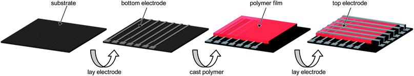 | ||
| Fig. 1 A schematic diagram of the fabrication process for a polymer memory device. | ||
Over the years, a large number of polymeric materials, including conjugated polymers, vinyl polymers with specific pendant groups, polyimides (PIs), polymer/organic molecule blends, polymer/metal hybrids, polymer/metal complexes, etc., have been reported to show bistable electrical switching properties.2,3 Considering the fabrication process requirements, among all the polymer systems, PI is thought to be one of the most suitable candidates for memory materials due to its outstanding thermal stability, chemical resistance, and mechanical strength.4 However, because of its high chemical resistance, PI exhibits a low solubility in the common organic solvents. Therefore, in general, thermal imidization is carried out by heating the precursor poly(amic acid) (PAA) film to obtain a PI film. By this method, intermolecular imidization is promoted and also the packing behavior highly depends on the film-forming method. Both phenomena might significantly change the electrical performance of the polymer.5 Hence, the design of a soluble PI, while maintaining a high thermal stability, mechanical strength and exhibiting good memory properties, is highly required.
In 2006, Kang et al. reported the first soluble PI (TP6F-PI) consisting of triphenylamine (TPA) and phthalimide units as the electron donor (D) and acceptor (A) moieties, respectively, showing bistable electrical switching properties (Fig. 2).8 The memory property was evaluated by constructing a simple indium–tin–oxide (ITO)/polymer/Al sandwich device, which is a typical structure of polymer memory devices (right side in Fig. 2). The observed memory property of TP6F-PI was the Dynamic Random Access Memory (DRAM) type and field-induced charge transfer (CT), probably similar to photo-induced CT, from the D moiety to the A moiety was considered to dominate the switching behavior. Moreover, TP6F-PI showed a high solubility in various common organic solvents, which makes it possible to obtain a PI film without the thermal conversion mentioned above. The hexafluoroisopropylidene (6F) group plays an important role in increasing the solubility of the PIs due to its bulkiness and low surface energy. Thus, the 4,4′-(hexafluoroisopropylidene)-diphthalimide (6FDI) unit has been widely used for the preparation of the PI memory.
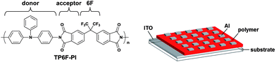 | ||
| Fig. 2 The chemical structure of TP6F-PI and a schematic diagram of a polymer memory device. | ||
During recent years, large numbers of PIs showing various kinds of memory properties, from volatile memory properties (DRAM, Static Random Access Memory (SRAM)) to non-volatile memory properties (FLASH, Write Once Read Many (WORM) type), have been reported. A volatile memory is a type of memory which cannot sustain the two distinct electronic states without an external electronic power supply, that is, the written data will disappear. On the other hand, a non-volatile memory can sustain the two distinct states without the power supply, that is, the written data will not disappear unless or even after an additional procedure is carried out. The control through these memory properties has been achieved by tuning the chemical structure of the D or A moieties. Therefore, understanding the relationship between the chemical structure and memory properties is a subject of utmost importance in the development of polymer memory materials. In this article, recent progress in the development of a resistive type PI memory is reviewed in three sections, mainly focusing on the effects of chemical structures on the memory properties. The first two sections will be classified depending on the mechanisms underlying the switching phenomena, which are field induced CT and filament formation. In the final section, fabrication processes toward the practical use of a resistive type PI memory device will be introduced. Materials other than PIs, device performance, and mechanisms have been widely reviewed elsewhere.3
2. Field induced CT effects in PI memory materials
In this section, the relationship between the structures of functional PIs and their memory properties from the viewpoint of a field induced CT will be discussed.2.1. Volatile DRAM and SRAM properties
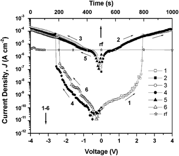
In 2009, Kang and co-workers reported a functional PI (PYTPA-PI) for application as a polymer memory material (Scheme 1).10 PYTPA-PI consists of TPA-substituted diphenylpyridine and 6FDI as the D and A moieties, respectively. The memory properties of PYTPA-PI were characterized by the current density–voltage (J–V) curve of an ITO/PYTPA-PI/Al sandwich device measured by a semiconductor analyzer (Fig. 3). In the 1st voltage sweep from 0 to 5 V, the current density is low in the range 10−8–10−6 A cm−2 until 2.7 V due to the insulating nature of the PYTPA-PI. However, a sharp increase is observed at around 2.7 V and then the current density is in the range of 10−2–10−1 A cm−2, indicating a switching behavior from the low conductivity (OFF) state to the high conductivity (ON) state. The electric transition from the OFF state to the ON state corresponds to the “writing” process of the current memory device. During the subsequent sweep from 0 to 5 V (2nd sweep), the ON state can be maintained at any voltage value, which means that two distinct conductivity states (OFF and ON) can be read at a low voltage value (e.g., below 2 V). In the 3rd voltage sweep from 0 to −2 V, the device remains in the ON state until −0.9 V. When the voltage becomes more negative, a sudden drop in the current density is observed and the device returns to the OFF state. This transition from the ON state to the OFF state serves as an “erasing” process for the current memory device. In the subsequent 4th sweep, the device remains in the OFF state at any voltage value from 0 to −2 V. As can be seen in the 5th and 6th sweeps, the ON state can be recovered by running the positive voltage sweep, indicating that the device is rewritable. However, by turning off the power for 1 min, the switched ON state returns to the initial OFF state without any erasing process (see the 7th sweep), which means that the device cannot sustain the ON state without the power supply and behaves as a volatile memory. The volatile ON state can be reprogrammed by reapplying a positive voltage over 2 V and be sustained by a refreshing voltage pulse of 2 V of 1 ms duration every 5 s (rf plots). Combining the writing, reading, erasing, rewriting, and refreshing ability shown above, the memory property of the PYTPA-PI is determined to be a volatile DRAM. Interestingly, when the applied voltage became more negative to −2.3 V after the 3rd sweep, the OFF state again switched to the ON state (see the 3rd sweep at Fig. 3b). This indicates that the device can be written bi-directionally and control of the negative sweep range, that is, 0 to −2 V, can avoid the rewriting behavior.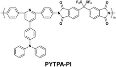 | ||
| Scheme 1 The chemical structure of PYTPA-PI. | ||
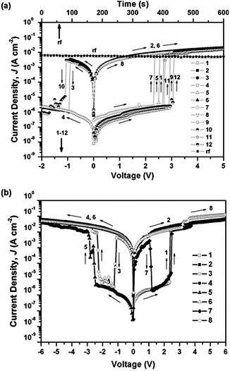 | ||
| Fig. 3 (a) The J–V curve of an ITO/PYTPA-PI/Al sandwich device and (b) J–V curve of the same device showing bi-directional electrical switching behavior. Reproduced with permission.10 Copyright 2009, American Institute of Physics. | ||
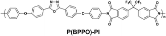
The same group also reported memory properties using a functional PI (P(BPPO)-PI) consisting of 2,5-bis(4-phenoxyphenyl)-1,3,4-oxadiazole (BPPO) and phthalimide as the D and A moieties, respectively (Scheme 2).14 In spite of the fact that an oxadiazole unit is usually adopted as the A moiety, the BPPO unit can act as a D moiety due to its lower electron affinity than the phthalimide. The memory properties characterized from the J–V curve (Fig. 4) of an ITO/P(BPPO)-PI/Al sandwich device are described below. During the 1st positive sweep from 0 to 4 V, a switching behavior from the OFF state to the ON state, corresponding to a “writing” process, is observed at around 2.3 V, and the induced ON state can be maintained during the subsequent 2nd sweep. Different to the PYTPA-PI, the ON state cannot be reset to the initial OFF state by sweeping the voltage in the reverse direction (3rd sweep), which means that P(BPPO)-PI is not erasable. Another difference between PYTPA-PI and P(BPPO)-PI is that the ON state of P(BPPO)-PI can be maintained for about 4 min after turning off the power supply. However, the ON state eventually returns to the initial OFF state, which means that the ON state is “remanent”, yet volatile. After the ON state has relaxed to the initial OFF state, it can be reswitched to the ON state by applying a negative voltage (the 4th sweep), which can remain when the subsequent negative voltage was repeated (5th sweep). Also, the ON state can be sustained by a refreshing voltage pulse of −1 V of 1 ms duration in every 5 s (the rf plots). Combining these results (the rewritable, refreshable, and also the “remanent”, yet volatile nature), P(BPPO)-PI can be considered as a Static Random Access Memory (SRAM), which can enable a low power consumption in real applications.
 | ||
| Scheme 2 The chemical structure of P(BPPO)-PI. | ||
 | ||
| Fig. 4 The J–V curve of an ITO/P(BPPO)-PI/Al sandwich device. Reprinted with permission from ref. 14. Copyright 2009, American Chemical Society. | ||
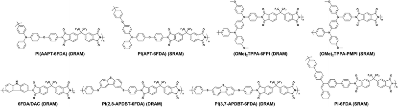
In 2010, our group reported two new TPA-based PIs, PI(AAPT-6FDA) and PI(APT-6FDA), which exhibited interesting memory properties (Scheme 3).16 The basic structures of these PIs are similar to the previously reported TP6F-PI, but possess mono- or dual-mediated phenoxy linkages (PL) in the repeating unit. The number of PLs obviously affected the resulting memory characteristics, as the PI(AAPT-6FDA) with a mono-PL shows DRAM properties, while PI(APT-6FDA) with a dual-PL shows SRAM properties. Recently, Liou and co-workers found that functional PIs containing the TPA derivative showed different kinds of memory properties by varying the connected A moiety.30,43 In this report, (OMe)2TPPA-6FDA exhibits DRAM property, while (OMe)2TPPA-PMPI shows SRAM property (Scheme 3). Besides, like P(BPPO)-PI, various kinds of functional PIs containing the D structure apart from the TPA derivatives were also found to exhibit DRAM or SRAM characteristics (Scheme 3). These D structures include carbazole (6FDA/DAC),21 dibenzothiophene (PI(2,8-APDBT-6FDA) and PI(3,7-APDBT-6FDA)),25 and triphenylethylene (PI-6FDA).39
 | ||
| Scheme 3 Chemical structures of the PIs showing volatile DRAM and SRAM properties. | ||
2.2. Non-volatile FLASH and WORM type memory properties
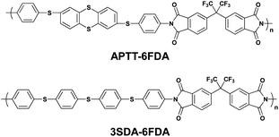
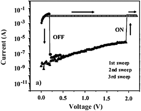
Compared to the volatile DRAM and SRAM behaviors, PIs showing non-volatile FLASH or WORM properties have mostly been developed quite recently from the view point of field induced CT effects. Also, unlike the volatile DRAM and SRAM, there are quite few reports about PIs showing non-volatile FLASH and WORM type memory characteristics.In 2009, our group reported memory-exhibiting functional PIs (APTT-6FDA and 3SDA-6FDA) comprised of thianthrene or phenylenethioether derivatives as the D moiety and 6FDI as the A moiety for application as a non-volatile memory (Scheme 4).12 Both PIs showed similar memory characteristics (Fig. 5). Taking APTT-6FDA for example (Fig. 5a), an abrupt increase in the current around 1.5 V was observed during the 1st voltage sweep corresponding to the “writing” process. The device remains in a high conductivity (ON) state during the subsequent 2nd sweep and also after turning off the power for more than 10 min, indicating non-volatile behavior. As the voltage is swept in the negative direction, a sudden decrease in the current around −3.2 V, corresponding to the “erasing” process, can be observed (3rd sweep) and the device remains in this low conductivity (OFF) state during the subsequent 4th sweep. The ON and OFF states can be reproduced by reapplying the switching threshold voltages (5th to 8th sweeps). Integrating the switching phenomena of the device and its volatility, the device based on APTT-6FDA can be used as a FLASH type memory.
 | ||
| Scheme 4 Chemical structures of APTT-6FDA and 3SDA-6FDA. | ||
 | ||
| Fig. 5 Current–voltage (I–V) curves of (a) APTT-6FDA, and (b) 3SDA-6FDA. Reprinted with permission from ref. 12. Copyright 2009, American Chemical Society. | ||
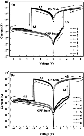
In 2010, Kang and co-workers also reported functional PIs (AZTA-PIa and OXTA-PIa) for non-volatile memory applications (Scheme 5).18,20 The D structures of AZTA-PIa and OXTA-PIa consist of TPA-substituted diphenyltriazole and TPA-substituted phenyloxadiazole, respectively, while the A structure is set to 6FDI. Like PYTPA-PI, the 1,2,4-triazole of AZTA-PIa and 1,3,4-oxadiazole of OXTA-PIa were introduced to enhance the CT process between the D and A moieties and affect the memory properties. The memory effect of the ITO/AZTA-PIa and OXTA-PIa/Al device demonstrated by the J–V curve (Fig. 6) is described below. During the initial voltage sweep, a “writing” process was observed around −2.5 and −1.5 V for AZTA-PIa and OXTA-PIa, respectively. The ON state can be maintained during the subsequent 2nd sweep and also after turning off the electrical power supply, which indicates non-volatile behavior. Moreover, different to APTT-6FDA and 3SDA-6FDA, the device cannot return to the initial OFF state even by applying the reverse voltage (3rd sweep). The non-erasable non-volatile switching behavior leads to the fact that the memory properties of AZTA-PIa and OXTA-PIa can be determined as the WORM type.
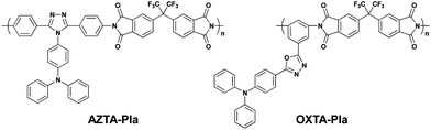 | ||
| Scheme 5 Chemical structures of AZTA-PIa and OXTA-PIa. | ||
 | ||
| Fig. 6 J–V curves of (a) AZTA-PIa and (b) OXTA-PIa. Reprinted with permission from ref. 18 and 20. Copyright 2010, American Chemical Society,18 Wiley.20 | ||
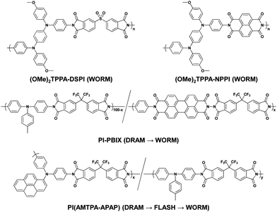
Recently, Liou's group reported that PIs containing the same D moiety to (OMe)2TPPA-6FDA connected with diphenylsulfonetetracarboxy diimide ((OMe)2TPPA-DSPI) or naphthalene diimide ((OMe)2TPPA-NPPI) showed a non-volatile WORM type memory (Scheme 6).43 Our group recently adopted random copolymers (coPI) containing perylene (PI-PBIX) or pyrene (PI(AMTPA-APAP)) to control the volatility of the resulting memory characteristics (Scheme 6).42,44 Both coPIs showed a memory characteristic transition from a volatile to non-volatile memory by increasing the content of the perylene or pyrene unit. For the PI-PBIX, the memory characteristics of the coPIs containing none or a small amount of the perylene unit (x = 0, 1, 2.5) showed volatile memory properties, while coPIs containing a larger amount of the perylene unit (x = 5, 10) showed non-volatile WORM type memory characteristics.42 As for PI(AMTPA-APAP), the memory properties changed from the volatile DRAM to the non-volatile FLASH type and to the non-erasable WORM type with the corresponding pyrene contents of 0, 5, and 100 mol%, respectively.44
 | ||
| Scheme 6 Chemical structures of PIs showing non-volatile characteristics. | ||
2.3. Mechanism and control of volatility
The mechanism underlying the switching phenomena of the functional PIs discussed above is consider to be dominated by the field induced CT theory, in which charges are transferred from the D moiety to A moiety under electrical bias and form a highly conductive CT state. To further understand this mechanism, the electronic states of the basic unit (BU) are often simulated by density functional theory (DFT) calculations. Fig. 7 shows the typical simulation results of the molecular orbital corresponding to each energy level of the BU of TP6F-PI using DFT calculations and the plausible electronic transitions under an electric field.8 As can be seen, the electron locating on the highest occupied molecular orbital (HOMO) (TPA unit) is locally excited to the 3rd lowest unoccupied molecular orbital (LUMO3) by applying an electric field higher than the threshold voltage. After the excitation, the electron is gradually transferred to LUMO2 and to LUMO, generating a CT state. This excitation can occur due to the overlapping of molecular orbitals around the TPA moiety at the HOMO and LUMO3. Also, a transition can directly occur from the HOMO to LUMO2 or to the LUMO. During this process, holes are generated at the HOMO, which produces an open channel for the charge carriers to migrate through. Therefore, a sharp increase occurs in the current density around the threshold voltage, indicating the electrical switching from the OFF state to the ON state.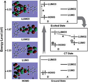 | ||
| Fig. 7 Calculated molecular orbitals, the corresponding energy levels of the BU, and plausible electronic transitions. Reprinted with permission from ref. 8. Copyright 2006, American Chemical Society. | ||
Taking the above mechanism into account, it is obvious that the stability of the CT state upon removal of the external electric power is the determining factor of the volatility. If the CT state is unstable under such a circumstance, the resulting memory characteristic would be a volatile one and vice versa. For the case of PIs showing DRAM properties, such as PYTPA-PI, due to the unstable CT state, the CT state immediately dissociates via the back CT or a recombination process of the separated charges after removing the power supply. Such dissociation can be delayed or prevented by several factors presented below.
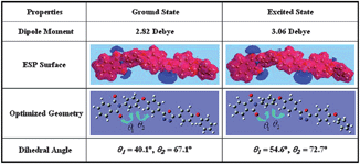 | ||
| Fig. 8 Optimized geometries of P(BPPO)-PI and dihedral angles between the component aromatic moieties at the ground state and excited state. Reprinted with permission from ref. 14. Copyright 2009, American Chemical Society. | ||
Extending this concept to a higher extent, the development of a non-volatile memory has been achieved. For example, for AZTA-PIa, the calculated dihedral angle between the phthalimide plane and neighboring benzene ring increased from 42.9° to 60.3° during the excitation (Fig. 9).20 This increase in the dihedral angle is much greater than that for TP6F-PI (42.1° to 43.9°)8 or P(BPPO)-PI (40.1° to 54.6°),14 which confirms that the energy barrier for the back CT of AZTA-PIa is much higher than that of TP6F-PI or P(BPPO)-PI and explains the non-volatile WORM type behavior.
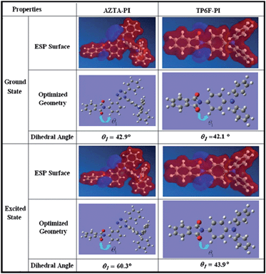 | ||
| Fig. 9 Optimized geometries of the BUs of AZTA-PI and TP6F-PI and the dihedral angles between the component aromatic moieties at the ground state and excited state. Reproduced with permission from ref. 20. Copyright 2010, Wiley. | ||
2.4. Other features
The evaluation of memory properties requires not only the J–V or I–V curve measurement but also endurance, retention stress, and write–read–erase–read (WRER) cycle tests. For instance, the retention times and stress tests of both the ON and OFF states of PI(APT-6FDA) are shown in Fig. 10a.16 Under a constant stress of −1 V, no obvious degradation in both ON and OFF states was observed for at least 104 s during the readout test. Also, both ON and OFF states were stable during the stimulus effect test for at least 108 continuous read pulses of −1 V (Fig. 10b).16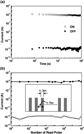 | ||
| Fig. 10 (a) Retention times under a continuous readout voltage and (b) the stimulus effect of read pulses on the ON and OFF states of the ITO/PI(APT-6FDA)/Al device. The inset of (b) shows the pulse shapes in the measurement. Reprinted with permission from ref. 16. Copyright 2010, American Chemical Society. | ||
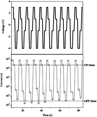
The WRER cycle test is required mostly in the case of FLASH type memory. Fig. 11 shows the typical WRER cycle test of 3SDA-6FDA.12 The write, read, erase, and reread voltages were set as 3.0, 1.0, −4.0, and −1.0 V, respectively. As can be seen, almost no degradation in both ON and OFF state was observed, indicating a high switching reproducibility.
 | ||
| Fig. 11 The applied voltage sequence and the typical current response to WRER cycles of 3SDA-6FDA. Reprinted with permission from ref. 12. Copyright 2009, American Chemical Society. | ||
To the best of our knowledge, similar to PI(APT-6FDA) and 3SDA-6FDA, all reported PIs showed high endurance to the constant voltage stress, continuous voltage pulse, and WRER cycles. Usually in organic and polymeric electronics, the oxidation and reduction processes during long term operation cause changes or, even worse, kill the original memory properties of the active materials.1 However, the above results clearly demonstrate that PIs possess high stability to the oxidation or reduction process and are suitable for long term operation. Moreover, it is possible to enhance such stability by encapsulating these active materials for practical use.
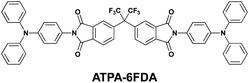
Since the beginning of the development of PI memory, almost all types of memory characteristics from volatile DRAM and SRAM to non-volatile FLASH and WORM types have been reported. These enthusiastic studies demonstrated that modulation of such memory properties can be achieved through design and chemical synthesis based on certain concepts, such as conformational changes, low lying LUMO energy, high dipole moment, and large conjugation. For the next stage of the PI memory development, we need to modulate every memory characteristic based on a universal design concept. To construct such a concept, systematic studies about the effect of the primary structure on the memory properties are still needed. For instance, one of the remaining factors to be investigated is the effect of molecular weight on the memory properties. Recently, we have reported that the small imide molecule (ATPA-6FDA) comprised of TPA and 6FDI exhibited non-volatile memory properties (Scheme 7).35 In spite of the fact that the chemical structure of ATPA-6FDA is the same as the repeating unit of TP6F-PI,8 the resulting memory properties were totally different. In this report, we have discussed the fact that the small molecule tends to have denser stacking and increases the molecular interaction with the adjacent molecules, which easily induces the formation of excimers and stabilizes the CT state. The problem of this argument is that there has never been a systematic study on the effect of molecular weight and the critical information of where the excimers are formed to stabilize the CT state is still unclear.
 | ||
| Scheme 7 The chemical structure of ATPA-6FDA. | ||
3. Filament formation in PI memory materials
In this second section, another theory, which is filament formation, will be discussed to explain the memory properties.3.1. Various memory properties
Since 2008, Ree et al. and other groups have reported a large variety of functional PIs showing excellent memory properties (Scheme 8). | ||
| Scheme 8 PIs developed from the view point of filament formation. | ||
For instance, the memory properties of 6F-2TPA PI, with a D structure of a tetraphenyl-substituted phenylenediamine, varied from the non-volatile WORM type to volatile DRAM depending on the film thickness and sweeping direction (Fig. 12).9 For a device based on a 15 nm 6F-2TPA PI film, a short circuit current flow is observed in both the positive and negative bias sweeps. The short circuit current flow in any negative voltage sweep was also observed when the film thickness increased to 34 nm. However, non-volatile WORM type memory characteristics were observed by applying a positive sweep. For a device using a 74 nm thick film, the WORM type memory behavior was observed in both the positive and negative voltage sweeps. This means that, for the 74 nm film thickness, the device shows a bipolar switching non-volatile WORM type memory behavior. By increasing the film thickness to 100 nm, the DRAM property, which is a completely different memory property compared to the 15, 34, 74 nm thick films, was observed during the negative sweep. Also, the switching behavior cannot be observed under the positive sweep indicating that the device with a 100 nm film thickness shows a unipolar switching volatile DRAM type memory. By further increasing the film thickness to 150 nm, no switching behavior can be observed during the positive or negative voltage sweep.
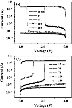 | ||
| Fig. 12 I–V curves of a Au/6F-2TPA PI/Al sandwich device using various thickness (15–150 nm) films; the voltage was swept to both (a) negative and (b) positive directions. Reproduced with permission.9 Copyright 2009, IOP Publishing Ltd. | ||
A similar film thickness effect was also reported by the same group using 6F-HTPA PI, in which the D structure is a hydroxyl-substituted triphenylamine.15 The threshold voltage of the device based on 6F-HTPA PI gradually increased from around 0.8 V to 1.6 V and to 2.7 V with the corresponding film thicknesses of 16, 30, and 54 nm, respectively (Fig. 13). In the same report, the effects of metal electrodes to the memory property were investigated as shown in Fig. 14. Despite the difference in bottom and top electrode pairs, the resulting memory characteristics were all WORM type. On the other hand, the threshold voltage varied with the electrode pairs and the sweep direction. Particularly, the threshold voltage significantly changed during the negative sweep (Fig. 14b). As the bottom electrode was changed from Al to Au and to ITO, the threshold voltage became more negative, from −2 V to −2.5 V and to −2.6 V, respectively. Such electrode effects were also observed in other reports.9,17 In addition, as shown in Fig. 15, the thermal stability of the 6F-HTPA PI-based device was tested under a nitrogen atmosphere. Under all temperatures from 20–150 °C, the device nicely showed WORM type memory properties. This means that the device has a large operating temperature range and does not break down even under a high operating temperature. As has been represented in Section 2–4, this result also demonstrates that PI is a suitable material for a robust memory device.
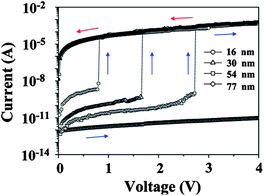 | ||
| Fig. 13 I–V curves of various thickness 6F-2HTPA PI films. Reprinted with permission from ref. 15. Copyright 2009, American Chemical Society. | ||
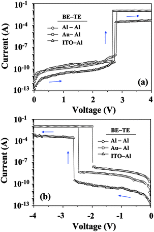 | ||
| Fig. 14 I–V curves of the device based on a 54 nm 6F-HTAP PI film fabricated with various bottom electrodes. The voltage was swept to both (a) positive and (b) negative directions. Abbreviation: BE, bottom electrode; TE, top electrode. Reprinted with permission from ref. 15. Copyright 2009, American Chemical Society. | ||
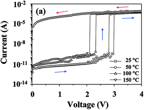 | ||
| Fig. 15 I–V curves measured for the ITO/6F-HTPA PI/Al device at various temperatures under a nitrogen atmosphere. Reprinted with permission from ref. 15. Copyright 2009, American Chemical Society. | ||
Ree et al. and Song et al. found that the switching behaviors of PIs having a pendant D type are dependent on the current compliance. Current compliance is a restriction of the current flow. As an illustration, when the current compliance is set to 0.01 A during the I–V measurements, the maximum current value flowing through the device will be limited to 0.01 A, no matter to how high the voltage is swept. From 2008 to 2011, five types of PIs, such as 6F-HAB-CBZ PI,7 6F-HAB-DPC PI,11 6F-HAB-TPAIE PI,13 MTPA-PI,17 and 6F-HAB-AM PI,24 which showed unique switching behaviors by controlling the current compliance, were reported (Scheme 8). Fig. 16 shows a typical I–V curve of a device based on 6F-HAB-CBZ PI. During the 1st positive voltage scan with the current compliance of 0.01 A, the device is at the low conductive OFF state from 0 to 1.5 V and changes to the high conductive ON state by further increasing the voltage to 2.1 V. The induced ON state can be maintained even after turning off the electrical power or during the subsequent positive sweep. Initially, the device seems to exhibit non-volatile WORM type memory characteristics. However, a sudden decrease from the ON state to the OFF state can be observed during the 3rd sweep with a current compliance of 0.1 A, which is 10 times higher than the current compliance for the “writing” process. This means that the “writing” and “erasing” processes in the memory device can be carried out by controlling the current compliance. The same switching behavior can also be observed during the negative sweep. Interestingly, this current compliance effect cannot be observed when the A structures are changed from 6FDA, i.e., PMDA, BPDA, ODPA, and DSDA.27
 | ||
| Fig. 16 I–V curves of 6F-HAB-CBZ PI. The current compliance of the first and second sweeps were set to 0.01 A, while the third sweep was set to 0.1 A. Reproduced with permission.7 Copyright 2008, Wiley. | ||
Recently, Ree's group reported the structural effects on the memory properties (chemical structures are shown in Scheme 8).38,40,41 By changing the substituents of the TPA moiety, the resulting memory properties dramatically changed. For example, the PI having a D structure of bis(trifluoromethyl)phenyl-substituted TPA (6F-TPA-F6 PI) showed volatile DRAM properties while the PI with the D structure of bithiophenyl-substituted TPA (6F-TPA-T2 PI) showed non-volatile WORM type memory properties.38 Besides, various kinds of pendent D structures (apart from the aryl amine) were also reported, like spiropyran,23 anthracene,24 and ferrocene.28
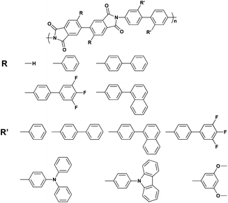
Since 2010, Shen and co-workers have reported a large variety of specific structured PIs for application as memory materials.22,29,33,34,37 The basic concept of their group is to induce a high ring torsion in the polymer backbone using the 2,2′-position aryl-substituted tetracarboxylic dianhydride and diamine (Scheme 9). Based on this concept, the solubility of the resulting polymers was satisfactory compared to the PI using the 6F unit and the variety of design had been expanded. More than 10 PIs were reported using this concept.
 | ||
| Scheme 9 Chemical structures of the PIs having a high ring torsion. | ||
3.2. Mechanism and the effects of film thickness, electrode, current compliance, and substituents
The mechanism underlying the switching behaviors and memory properties discussed above is thought to be filament formation. The D and A moieties act as nucleophilic and electrophilic sites, respectively, which can both serve as charge-trapping sites. Thus, when an electric field is applied to the functional PI, the D and A moieties are enriched with holes and electrons, respectively. After the applied bias reaches the threshold voltage, the trapped charges are able to move through the trapped sites by means of a hopping process. This phenomenon forms a conductive filament, which results in a current flow between the bottom and top electrodes.Based on this mechanism, the film thickness, electrode, current compliance, and substituent effects on the memory properties can be clearly explained, as given below. For 6F-2TPA PI,9 the HOMO and LUMO energy levels are −5.10 and −1.88 eV, respectively, while the work function of the Au and Al electrodes are −5.1 and −4.2 eV, respectively. When the film thickness is 15 nm, the thickness is too thin and the positive or negative bias can easily override the energy barrier between the work function of the electrodes and HOMO–LUMO energy levels, resulting in a short circuit current flow. For the 34 nm one, the film is thick enough to generate an energy barrier between the work function of the Al electrode and the LUMO energy level, which prevents a short circuit in the positive flow. However, the short circuit current flow is still observed during the negative voltage sweep due to the zero energy barrier between the work function of the Au electrode and the HOMO energy level. As a result, the device using the 34 nm 6F-2TPA-PI film shows a unipolar switching non-volatile WORM type memory. By increasing the thickness to 74 nm, the films become thick enough to prevent a short circuit in either sweeping direction. Thus, the device shows a bipolar switching non-volatile WORM type memory. The threshold voltage of the negative sweep is lower than that of the positive sweep (−1.8 and 2.1 V, respectively). This is because the energy barrier between the work function of the Au electrode and HOMO energy level is smaller than the barrier between the work function of Al electrode and the LUMO energy level. When it comes to a 100 nm film thickness, the film becomes too thick to form a stable conductive filament and the device shows volatile DRAM type memory behavior during the negative sweep. However, due to the high energy barrier between the work function of the Al electrode and the LUMO energy level, a conductive filament cannot be formed in this film thickness and results in no switching behavior during the positive voltage sweep. Finally, by increasing the film thickness to 150 nm, the thickness becomes high enough to prevent the formation of a conductive filament. Therefore, no switching behavior can be observed during both the positive and negative voltage sweeps. As for 6F-HTPA PI,15 the 16–54 nm films are thick enough to prevent any short circuit and can exhibit stable WORM type memory characteristics. However, as the film thickness increases, the formation of a conductive filament becomes more difficult and needs more energy. Thus, the threshold voltage increases with an increase in the film thickness.
The relationship between the bottom and top electrode pairs and the threshold voltage can also be discussed by comparing the HOMO–LUMO energy levels of the polymers and the work functions of the electrodes. Taking 6F-HTPA PI as an example,15 the HOMO and LUMO energy levels of the polymer are −5.26 and −2.26 eV, respectively, while the work functions of Al, ITO, and Au are −4.30, −4.80, and −5.20 eV, respectively (shown in Fig. 17). During the positive sweep, the top electrode acts as a cathode and hole injection occurs from the top Al electrode to the HOMO energy level of 6F-HTPA PI. Thus, during this sweep direction, the energy barrier between the electrode and the HOMO energy level is constant regardless of the bottom electrode, resulting in a small fluctuation in the threshold voltage (Fig. 14a). On the other hand, during the negative voltage sweep, the bottom electrode acts as a cathode and the energy barrier between the work function of the electrode and the HOMO energy level varies with the bottom electrodes, resulting in a large fluctuation in the threshold voltage. Since the energy barriers between the work function of the electrode decrease as the bottom electrode changes from Al to ITO and to Au, the device using an Al–Al electrode pair shows the highest threshold voltage, while the threshold voltage of the device using a Au–Al electrode pair has the smallest value during the negative voltage sweep (Fig. 14b). However, since the switching mechanism is based on the formation of a conductive filament, which is independent of the electrode, the electrode pair does not change the fundamental memory property of the PIs.
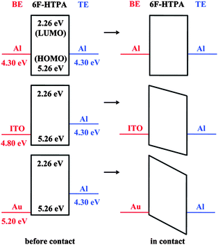 | ||
| Fig. 17 Energy level diagrams of 6F-HTPA PI and various electrodes. Reprinted with permission from ref. 15. Copyright 2009, American Chemical Society. | ||
Similar to the film thickness effects, the relationship between the current compliance and switching behavior can also be explained by the filament formation mechanism.7,11,13,17,24 When a bias is applied with a high current level (i.e., current compliance set to 0.1 A), a high number of charges will be injected into the formed filament, which overloads the capacity of the filament. The excess injected charges produce additional heat, which ruptures the conductive filament, resulting in an abrupt decrease in the conductivity. However, for PMDA-HAB-CBZ, BPDA-HAB-CBZ, ODPA-HAB-CBZ, and DSDA-HAB-CBZ,27 the electron accepting ability of the four PIs are quite low compared to 6F-HAB-CBZ PI.7 Therefore, the D and A moieties could not properly act as charge trapping sites and the resulting filament was insensitive to the current compliance.
The substituent effect on the memory properties can be illustrated similar to the field induced CT mechanism. For the case of 6F-TPA-F6 PI, the bis(trifluoromethyl)phenyl substituent is a strong electron accepting moiety, which intensely reduces the nucleophilicity of the TPA. Therefore, the charge trapping ability of the D moiety is not sufficient to form a definite filament, resulting in volatile DRAM behavior. On the other hand, the bithiophene substituent in 6F-TPA-T2 PI is a strong electron donating moiety and also possesses large conjugation. These typical features of bithiophene enhance the charge trapping ability of the D moiety. Thus the formed filament is strong enough to exhibit non-volatile WORM type memory.38
So far, by controlling the film thickness and measurement conditions, such as the current compliance, or carefully designing the primary structure, almost all types of memory properties can be developed and these memory properties showed very high reproducibility (Fig. 15) and stability to the long term operation (measurements are represented in section 2.4). These achievements are similar to the field induced CT mechanism. However, the exact observation of the conductive filament has not yet been carried out. Such a problem can be referred to in the case of the field induced CT mechanism, although the formation of the CT state can be indirectly observed by using spectroscopic measurements.14 Also, similar to the CT mechanism, it is predictable that molecular weight might affect the formation of the conductive filament. For the future development of PI memory materials from the view point of filament formation, further investigations of the structural effects on the formation of filaments are still needed.
4. Approaches for practical use of PI memory devices
In the final section, taking advantage of the polymeric materials, such as solution processability and flexibility, the device fabrication process for practical use of the PI memory will be briefly introduced.4.1. Three-dimensional device
In 2010, Lee and co-workers reported a three-dimensionally integrated PI memory device possessing 192 memory cells (8 × 8 × 3) in a single device (Fig. 18a).19 A blend system of 6-phenyl-C61 butyric acid methyl ester (PCBM) and PI prepared from biphenyl dianhydride and phenylenediamine was used as an active layer in this device. The memory cell of each layer showed bipolar non-volatile memory properties (Fig. 18b(1)). Surprisingly, over 83% of the memory cells operated without any malfunction (56 cells out of 64 in the first and second layers and 48 out of 64 in the third layer; overall, 160 out of 192 cells). The inoperative memory cells were found to lie along a common electrode. Therefore, a more careful forming process can produce fewer malfunctioning memory cells and enables high-density integration of organic memory devices.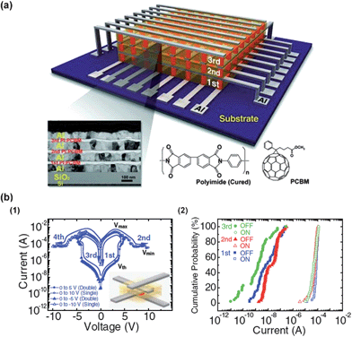 | ||
| Fig. 18 (a) A schematic illustration of the three-dimensional PI memory device. The lower part shows the cross-section TEM and the chemical structures of the active materials. (b) (1) Typical I–V cures of the active layer and (2) cumulative probability data for all operative cells (160 operative cells out of 192 fabricated cells). Reproduced with permission.19 Copyright 2010, Wiley. | ||
Another important feature in this research area is the readout margin. A readout margin is kind of a surplus for the device to demonstrate a prescribed performance under the worst conditions. Fig. 18b(2) shows the cumulative probability of the switching currents of all the operative memory cells in each layer. The distribution of the currents at the ON state lies within about an order of magnitude, while the distribution of OFF state currents is rather broad. The most important point in this result is that the ON and OFF currents are separated by more than one order of magnitude. This separation provides a readout margin.
4.2. Small scale and high density devices
In 2011, a very small and dense memory device with a junction size of 2 μm was reported by Lee et al., as shown in Fig. 19.26 In this study, the same material as described above was used as the active layer and a direct metal-transfer method was adopted to obtain such a device. Like the three-dimensional device, this small and dense device also showed a high yield of operating memory cells (50 cells out of 64). Also, the distribution of the currents at the ON and OFF states was well separated by the range of 103, which is much higher than that of the three-dimensional device shown in Fig. 18b(2), showing a sufficient memory margin (Fig. 19b). Moreover, by further decreasing the size of the device, the authors reached a junction size of 100 nm.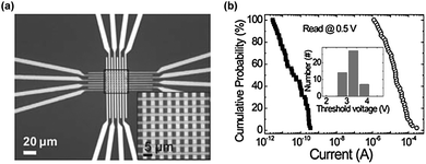 | ||
| Fig. 19 (a) An optical image of a 2 μm-scale memory device in an 8 × 8 array structure. (b) A I–V curve of the 100 nm-scale device. Reproduced with permission.26 Copyright 2011, Wiley. | ||
Another approach to achieving a small scale and high density memory device is by applying the scanning probe microscope (SPM) technique, which was reported by Yoshida's group32 and Zhuge's group.36 By using this method, an extremely dense memory cell can be prepared. For example, by applying a 500 ms pulsed voltage of 5 V to the PI film using the SPM technique, a dot pattern with an average diameter and pitch of 30 and 50 nm, respectively, was obtained.32 The estimated data storage density was approximately 250 Gbit inch−2 (Fig. 20).
 | ||
| Fig. 20 (a) A conductive image of the PI film after dot pattern modification. (b) The current profile along C–C′ in (a). Reproduced with permission.32 Copyright 2010, IOP Publishing Ltd. | ||
4.3. Flexible devices
Similar to other organic electronics, the flexible polymer memory device has also been demonstrated using PI as an active layer. In 2011, Lee and co-workers fabricated a memory device similar to the previous ones19,26 on a flexible poly(ethyleneterephthalate) (PET) substrate.31 The device showed a very stable non-volatile behavior even after bending at a radius curvature of 4.2 mm and also up to 10![[thin space (1/6-em)]](https://www.rsc.org/images/entities/char_2009.gif) 000 bending cycles (Fig. 21). Also, similar to the device presented in section 4.1 and 4.2, the statistical distribution of the ON and OFF states of this device was well separated.
000 bending cycles (Fig. 21). Also, similar to the device presented in section 4.1 and 4.2, the statistical distribution of the ON and OFF states of this device was well separated.
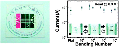 | ||
| Fig. 21 An optical image of the memory device (left side) and the bending test results (right side). Reprinted with permission from ref. 31. Copyright 2011, American Chemical Society. Caption. | ||
Recently, our group also reported a flexible memory device fabricated on a flexible poly(ethylenenaphthalate) (PEN) substrate using PI(AMTPA-APAP) as an active layer.44 The device performance was similar to that fabricated on a non-flexible glass substrate and its performance could be maintained even by bending at a radius of 5 mm.
The development of device fabrication for practical use has been carried out to a large extent. Like other organic electronics, such as organic transistors, organic photovoltaics, etc., the performance of a polymer memory should significantly rely on the fabrication process of the device. Therefore, similar to the development of the memory material itself, there is still significant potential in this area.
5. Summary
The development of polymer materials for application to low processing cost, flexible, and high density data storage devices is an emerging area. One of the best candidates for such a material is PI. In this review, we have seen that energetic research around the world has shown a great possibility for the future application of PI as a memory device material. Although the structure and operating mechanism of the memory device is quite simple, that is, the sandwich device structure and using the conductivity response, the mechanism underlying the switching behavior of the functional material is extremely complicated. So far, two major theories have been used to explain such phenomena and have been working well to a great extent. By carefully designing the polymer structure based on these theories, almost all kinds of current memory characteristics can be reproduced in the PI memory device, as summarized in Table 1. Also, without exception, these memory properties show extremely high endurance during long term operation, which again makes PI a very suitable material for memory applications. Moreover, the successful research on fabricating various kinds of devices like three-dimensional,19 small and dense,26,32 and flexible devices31,44 will accelerate the practical use of PI as memory materials. However, there still remain a number of issues to be solved. One of the big problems is that the considerations of the resulting memory properties and their mechanism include many speculations. No conclusive evidence for the key factors of the switching behavior of the CT state or the conductive filament has been observed. Another serious issue is that there seems to be no boundary between the two represented theories. To be more specific, looking from the structural point of view between the two major theories, the resulting memory properties are completely different, although the chemical structures are quite similar. For example, the structures of (OMe)2TPPA-6FPI (reported by Liou's group)30,43 and 6F-2TPA PI (reported by Lee's group)9 are almost the same, while the memory characteristics are DRAM and WORM type, respectively. One way to distinguish these two theories is to measure the dependence of the ON state current on the cell size (in other words, contact area of the electrode). In most cases, the evaluation of the memory properties is carried out using a variety of sizes of Al electrode. For instance, in the report of PYTPA-PI, the size of the Al electrodes were 0.2 × 0.2 and 0.4 × 0.4 mm2.10 When the switching behavior is based on the CT theory, the ON state current value is proportional to the contact area.10,14,18 On the other hand, the ON state in the filament formation theory is independent of the contact area.9,15,22,33,38,40,41 Although this diagnosis is a simple and effective way to distinguish the two theories, the reason why the CT state and conductive filament are dependent and independent, respectively, on the contact area has not been fully investigated. Therefore, the relationship between the polymer structure and the resulting memory characteristic still remains unclear. In future developments, the switching phenomena should be systematically investigated from both points of view and perhaps a dominating mechanism covering both theories might be established.| Mechanism | PI | Type of memory | Remarks | Ref. |
|---|---|---|---|---|
| CT | TP6F-PI | DRAM | — | 8 |
| PYTPA-PI | DRAM | — | 10 | |
| PI(AAPT-6FDA) | DRAM | — | 16 | |
| (OMe)2TPPA-6FPI | DRAM | — | 30,43 | |
| P(BPPO)-PI | SRAM | Torsional angle | 14 | |
| PI(APT-6FDA) | SRAM | Torsional angle | 16 | |
| (OMe)2TPPA-PMPI | SRAM | LUMO energy | 43 | |
| APTT-6FDA | FLASH | Dipole moment | 12 | |
| 3SDA-6FDA | FLASH | Dipole moment | 12 | |
| AZTA-PIa | WORM | Torsional angle | 20 | |
| OXTA-PIa | WORM | Torsional angle | 18 | |
| (OMe)2TPPA-DSPI | WORM | Dipole moment | 43 | |
| (OMe)2TPPA-NPPI | WORM | LUMO energy | 43 | |
| PI-PBIX | DRAM → WORM | Resonance effect | 42 | |
| PI(AMTPA-APAP) | DRAM → FLASH → WORM | Resonance effect | 44 | |
| FF | 6F-2TPA PI | WORM → DRAM | Film-thickness dependence | 9 |
| 6F-HTPA PI | WORM | Film-thickness dependence | 15 | |
| 6F-HAB-CBZ PI | Non-volatile | Compliance current | 7 | |
| 6F-HAB-DPC PI | Non-volatile | Compliance current | 11 | |
| 6F-HAB-TPAIE PI | Non-volatile | Compliance current | 13 | |
| MTPA-PI | Non-volatile | Compliance current | 17 | |
| 6F-HAB-AM PI | Non-volatile | Compliance current | 24 | |
| 6F-TPA-F6 PI | DRAM | Substitution effect | 38 | |
| 6F-TPA-T2 PI | WORM | Substitution effect | 38 |
Notes and references
- International Technology Roadmap for Semiconductors, http://www.itrs.net/Links/2011ITRS/Home2011.htm, 2011 Search PubMed.
- Q. D. Ling, D. J. Liaw, E. Y. H. Teo, C. Zhu, D. S. H. Chan, E. T. Kang and K. G. Neoh, Polymer, 2007, 48, 5182 CrossRef CAS.
- Q. D. Ling, D. J. Liaw, C. Zhu, D. S. H. Chan, E. T. Kang and K. G. Neoh, Prog. Polym. Sci., 2008, 33, 917 CrossRef CAS.
- F. Claudius and F. Hilmar, Polyimides in High-performance Electronics Packaging and Optoelectronic Applications, in Polyimides: Fundamentals and Applications, ed. M. K. Ghosh and K. L. Mittal, New York, Marcel Dekker, 1996, p. 759 Search PubMed.
- P. Leisieur, A. Barraud and M. Vandevyver, Thin Solid Films, 1987, 152, 155 CrossRef.
- I. Cacelli, A. Ferretti, M. Girlanda and M. Macucci, Chem. Phys., 2006, 320, 84 CrossRef CAS.
- S. G. Hahm, S. Choi, S. H. Hong, T. J. Lee, S. Park, D. M. Kim, W. S. Kwon, K. Kim, O. Kim and M. Ree, Adv. Funct. Mater., 2008, 18, 3276 CrossRef CAS.
- Q. D. Ling, F. C. Chang, Y. Song, C. X. Zhu, D. J. Liaw, D. S. H. Chan, E. T. Kang and K. G. Neoh, J. Am. Chem. Soc., 2006, 128, 8732 CrossRef CAS.
- T. J. Lee, C. W. Chang, S. G. Hahm, K. Kim, S. Park, D. M. Kim, J. Kim, W. S. Kwon, G. S. Liou and M. Ree, Nanotechnology, 2009, 20, 135204 CrossRef.
- Y. L. Liu, Q. D. Ling, E. T. Kang, K. G. Neoh, D. J. Liaw, W. T. Liou, C. X. Zhu and D. S. H. Chan, J. Appl. Phys., 2009, 105, 044501 CrossRef.
- S. G. Hahm, S. Choi, S. H. Hong, T. J. Lee, S. Park, D. M. Kim, J. C. Kim, W. Kwon, K. Kim, M. J. Kim, O. Kim and M. Ree, J. Mater. Chem., 2009, 19, 2207 RSC.
- N. H. You, C. C. Chueh, C. L. Liu, M. Ueda and W. C. Chen, Macromolecules, 2009, 42, 4456 CrossRef CAS.
- K. Kim, S. Park, S. G. Hahm, T. J. Lee, D. M. Kim, J. C. Kim, W. Kwon, Y. G. Ko and M. Ree, J. Phys. Chem. B, 2009, 113, 9143 CrossRef CAS.
- Y. L. Liu, K. L. Wang, G. S. Huang, C. X. Zhu, E. S. Tok, K. G. Neoh and E. T. Kang, Chem. Mater., 2009, 21, 3391 CrossRef CAS.
- D. M. Kim, S. Park, T. J. Lee, S. G. Hahm, K. Kim, J. C. Kim, W. Kwon and M. Ree, Langmuir, 2009, 25, 11713 CrossRef CAS.
- T. Kuorosawa, C. C. Chueh, C. L. Liu, T. Higashihara, M. Ueda and W. C. Chen, Macromolecules, 2010, 43, 1236 CrossRef CAS.
- Q. Liu, K. Jiang, L. Wang, Y. Wen, J. Wang, Y. Ma and Y. Song, Appl. Phys. Lett., 2010, 96, 213305 CrossRef.
- K. L. Wang, Y. L. Liu, J. W. Lee, K. G. Neoh and E. T. Kang, Macromolecules, 2010, 43, 7159 CrossRef CAS.
- S. Song, B. Cho, T. W. Kim, Y. Li, M. Jo, G. Wang, M. Choe, Y. H. Kahng, H. Hwang and T. Lee, Adv. Mater., 2010, 22, 5048 CrossRef CAS.
- K. L. Wang, Y. L. Liu, I. H. Shin, K. G. Neoh and E. T. Kang, J. Polym. Sci., Part A: Polym. Chem., 2010, 48, 5790 CrossRef CAS.
- G. Tian, D. Wu, S. Qi, Z. Wu and X. Wang, Macromol. Rapid Commun., 2011, 32, 384 CrossRef CAS.
- Y. Li, H. Xu, X. Tao, K. Qian, S. Fu, Y. Shen and S. Ding, J. Mater. Chem., 2011, 21, 1810 RSC.
- Q. Liu, K. Jiang, Y. Wen, J. Wang, J. Luo and Y. Song, Appl. Phys. Lett., 2010, 97, 253304 CrossRef.
- S. Park, K. Kim, D. M. Kim, W. Kwon, J. Choi and M. Ree, ACS Appl. Mater. Interfaces, 2011, 3, 765 CAS.
- C. L. Liu, T. Kurosawa, A. D. Yu, T. Higashihara, M. Ueda and W. C. Chen, J. Phys. Chem. C, 2011, 115, 5930 CAS.
- J. J. Kim, B. Cho, K. S. Kim, T. Lee and G. Y. Jung, Adv. Mater., 2011, 23, 2104 CrossRef CAS.
- S. Park, K. Kim, J. C. Kim, W. Kwon, D. M. Kim and M. Ree, Polymer, 2011, 52, 2170 CrossRef CAS.
- G. Tian, S. Qi, F. Chen, L. Shi, W. Hu and D. Wu, Appl. Phys. Lett., 2011, 98, 203302 CrossRef.
- Y. Li, H. Xu, X. Tao, K. Qian, S. Fu, S. Ding and Y. Shen, Polym. Int., 2011, 60, 1679 CrossRef CAS.
- C. J. Chen, H. J. Yen, W. C. Chen and G. S. Liou, J. Polym. Sci., Part A: Polym. Chem., 2011, 49, 3709 CrossRef CAS.
- Y. Ji, S. Lee, B. Cho, S. Song and T. Lee, ACS Nano, 2011, 5, 5995 CrossRef CAS.
- S. Yoshida, T. Ono and M. Esashi, Nanotechnology, 2011, 22, 335302 CrossRef.
- Y. Q. Li, R. C. Fang, A. M. Zheng, Y. Y. Chu, X. Tao, H. H. Xu, S. J. Ding and Y. Z. Shen, J. Mater. Chem., 2011, 21, 15643 RSC.
- Y. Li, R. Fang, S. Ding and Y. Shen, Macromol. Chem. Phys., 2011, 212, 2360 CrossRef CAS.
- W. Y. Lee, T. Kurosawa, S. T. Lin, T. Higashihara, M. Ueda and W. C. Chen, Chem. Mater., 2011, 23, 4487 CrossRef CAS.
- B. Hu, F. Zhuge, X. Zhu, S. Peng, X. Chen, L. Pan, Q. Yan and R. W. Li, J. Mater. Chem., 2012, 22, 520 RSC.
- Y. Li, Y. Chu, R. Fang, S. Ding, Y. Wang, Y. Shen and A. Zheng, Polymer, 2012, 53, 229 CrossRef CAS.
- D. M. Kim, Y. G. Ko, J. K. Choi, K. Kim, W. Kwon, J. Jung, T. H. Yoon and M. Ree, Polymer, 2012, 53, 1703 CrossRef CAS.
- Y. Liu, Y. Zheng, Q. Lan, S. Liu, Z. Qin, L. Chen, C. Zhao, Z. Chi, J. Xu and J. Economy, Chem. Mater., 2012, 24, 1212 CrossRef CAS.
- T. J. Lee, Y. G. Ko, H. J. Yen, K. Kim, D. M. Kim, W. Kwon, S. G. Hahm, G. S. Liou and M. Ree, Polym. Chem., 2012, 3, 1276 RSC.
- Y. G. Ko, W. Kwon, H. J. Yen, C. W. Chang, D. M. Kim, K. Kim, S. G. Hahm, T. J. Lee, G. S. Liou and M. Ree, Macromolecules, 2012, 45, 3749 CrossRef CAS.
- T. Kurosawa, Y. C. Lai, T. Higashihara, M. Ueda, C. L. Liu and W. C. Chen, Macromolecules, 2012, 45, 4556 CrossRef CAS.
- C. J. Chen, H. J. Yen, W. C. Chen and G. S. Liou, J. Mater. Chem., 2012, 22, 14085 RSC.
- A. D. Yu, T. Kurosawa, Y. C. Lai, T. Higashihara, M. Ueda, C. L. Liu and W. C. Chen, J. Mater. Chem., 2012, 22, 20754 RSC.
| This journal is © The Royal Society of Chemistry 2013 |