 Open Access Article
Creative Commons Attribution 3.0 Unported Licence
Hysteresis in memristors produces conduction inductance and conduction capacitance effects
Juan
Bisquert
 *a,
Juan B.
Roldán
 b and
Enrique
Miranda
c
aInstitute of Advanced Materials (INAM), Universitat Jaume I, 12006 Castelló, Spain. E-mail: bisquert@uji.es
bDepartamento de Electrónica y Tecnología de Computadores, Universidad de Granada, Facultad de Ciencias, Avd. Fuentenueva s/n, 18071 Granada, Spain
cDept. Enginyeria Electrònica, Universitat Autònoma de Barcelona, 08193 Cerdanyola del Vallès, Spain
First published on 15th April 2024
Abstract
Memristors are devices in which the conductance state can be alternately switched between a high and a low value by means of a voltage scan. In general, systems involving a chemical inductor mechanism as solar cells, asymmetric nanopores in electrochemical cells, transistors, and solid state memristive devices, exhibit a current increase and decrease over time that generates hysteresis. By performing small signal ac impedance spectroscopy, we show that memristors, or any other system with hysteresis relying on the conductance modulation effect, display intrinsic dynamic inductor-like and capacitance-like behaviours in specific input voltage ranges. Both the conduction inductance and the conduction capacitance originate in the same delayed conduction process linked to the memristor dynamics and not in electromagnetic or polarization effects. A simple memristor model reproduces the main features of the transition from capacitive to inductive impedance spectroscopy spectra, which causes a nonzero crossing of current–voltage curves.
Memristive devices are being widely investigated for different applications related to non-volatile memory storage, neuromorphic computational systems, hardware cryptography and radio-frequency switches.1–8 Memristors are often defined by equations of the type9–13
| Itot = f(V, λ) | (1) |
 | (2) |
Eqn (1) is a current–voltage Itot–V characteristic that depends on a state variable λ. This variable imparts memory characteristics to the system via relaxation dynamical equation eqn (2). The adaptation of λ is delayed with respect to the changes of the stimulus of the external voltage. By the delay effect (incremental form) of eqn (2), memristors always show hysteresis.
Memristors, as described by eqn ((1) and (2)), are usually associated with the properties of resistive switching,13 often connected with the formation and partial disruption of a nonvolatile conduction filament (in the most general case of filamentary switching) in the insulator layer that separates metal electrodes. However, a larger class of systems are also described by these equations. For example, solar cells, protein channels, and transistors show hysteresis,14–21 while the resistance memory is not the main functionality, and are normally not associated with resistive switching. To provide a more general account of these properties, we have termed a chemical inductor as any conduction system described by eqn ((1) and (2)).22 The central paradigm of the chemical inductor, and historically the original formulation, is given by the Hodgkin–Huxley equations that describe the temporal dynamics of action potentials in neurons.23–26
Memristors are usually characterized by a self-crossing current–voltage curve under a dynamic scan of voltage. This is because the current raises in one polarity, e.g. at a positive voltage, which is called a SET process, and in the return RESET process at negative polarity, the current returns to a low value. An example of the experimental measurement of rectifying nanopores in electrochemical cells18,27,28 is shown in Fig. 1.29
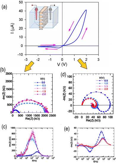 | ||
| Fig. 1 (a) Current–voltage curve measured at a frequency of Ωs = 10 Hz for a multipore membrane in 100 mM KCl solution at a neutral pH. The inset shows the electrochemical cell with the membrane. (b) The impedance spectra at different reverse voltages, with the corresponding bode plot of the imaginary part of the impedance in (c). (d) and (e) The impedance spectra and bode plots at a forward voltage. Adapted from P. Ramirez, J. Cervera, S. Nasir, M. Ali, W. Ensinger and S. Mafe, Electrochemical impedance spectroscopy of membranes with nanofluidic conical pores, J. Colloid and Interface Sci., 2024, 655, 876–885, with permission from Elsevier.29 | ||
In this paper, we discuss the frequency domain response of memristors and self-crossing chemical inductors, in general, and we analyze the relationship of such properties with the hysteresis features. We show here that for a system described by eqn ((1) and (2)), there are certain regions of operation where one might interpret a measurement of a memristor to be a capacitor and in other regions to be an inductor. We emphasize that there is no real capacitor or inductor (i.e., no sub-components with a Q–V or Flux–I relationships). Rather, a memristor behaves in “capacitor-like” and “inductor-like” manners. This result is obtained by representing the small signal ac impedance response of the memristor in the typical form of an equivalent circuit.30–34
It has been possible to classify the types of hysteresis displayed by memristors.35 In a set cycle, where the conductance changes to a high value, the I–V curve makes a counter clockwise loop. The hysteresis is inductive (or inverted), see Fig. 1a, for positive voltages.36–42 In contrast, in the reset cycle, the current decreases and the hysteresis is capacitive, making a clockwise loop, see Fig. 1a at negative voltages. Furthermore, it has been shown that the small signal ac impedance characteristics reveal the type of hysteresis inherent to the dynamical properties of the model.35 The inductive characteristic, represented by the arc in the fourth quadrant of the complex impedance plane related to the counter clockwise cycle of the current–voltage in the positive voltages, is reported in Fig. 1d. Contrarily, in the negative side, the impedance is fully capacitive and associated with the clockwise reset loop.
The inductive feature of impedance spectroscopy has been observed in different types of all-solid memristors.42–46Fig. 2 shows the huge inductive arcs of a halide perovskite memristor. This is the famous “negative capacitance” of solar cells,47–50 which has been connected to inverted hysteresis36,37,51 that here we also term inductive hysteresis.35 In Fig. 3, the conductance and susceptance of a TiN/Ti/HfO2/W resistive RAM memory device are shown.46 It is observed that when the conductance switches between low (OFF state) and high (ON state), the susceptance changes respectively between positive (capacitive) and negative (inductive).
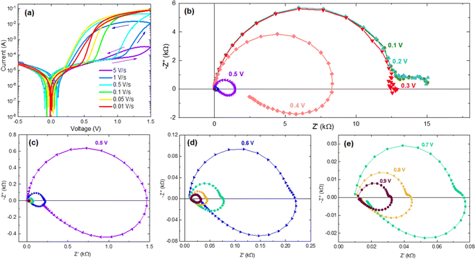 | ||
| Fig. 2 (a) Current–voltage characteristics of the halide perovskite memristor device FTO/poly(3,4-ethylenedioxythiophene) polystyrene sulfonate (PEDOT:PSS)/CH3NH3PbI3/Au at 6 different scan rates starting from 5 V s−1. Arrows indicate the sweep direction. (b)–(e) Complex plane plot representation of the impedance spectra at different applied dc voltages. (c)–(e) Plots corresponding to a magnification of the scales. M. Berruet, J. C.Pérez-Martínez, B. Romero, C. Gonzales, A. M. Al-Mayouf, A. Guerrero and J. Bisquert, Physical model for the current–voltage hysteresis and impedance of halide perovskite memristors. ACS Energy Lett., 2022, 7, 1214–1222; licensed under a Creative Commons Attribution (CC BY) license.43 | ||
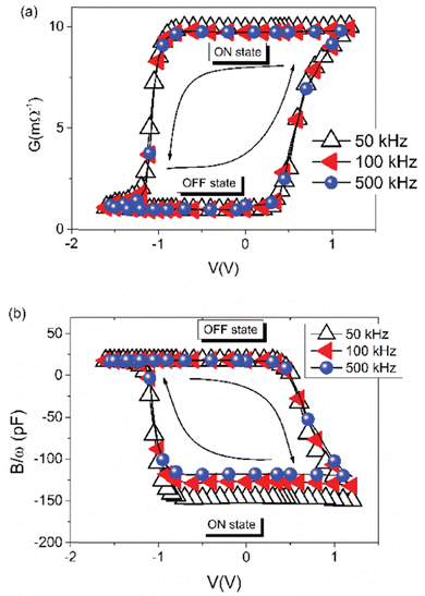 | ||
| Fig. 3 Conductance (a) and susceptance (b) of the TiN/Ti/HfO2/W resistive RAM memory device measured at 0 volts vs. programming voltage at three frequencies. An increasing and decreasing voltage steps applied in the range in which the device switches. Between the steps, the impedance is measured at zero voltage, applying only the small ac signal to avoid introducing disturbance. Reproduced by permission from S. Dueñas, H. Castán, H. García, Ó. G. Ossorio, L. A. Domínguez, and E. Miranda, Experimental Observation of Negative Susceptance in HfO2-Based RRAM Devices, IEEE Electron Device Lett., 2017, 38, 1216–1219.46 | ||
The appearance of a large inductor in systems that do not contain any internal electromagnetic inductor has been remarked in many research fields, e.g. in solar cells,47–50 corrosion systems,52,53 and proton exchange membrane (PEM) fuel cells.54–56 Since the early part of the 20th century, people have modeled many systems (e.g., biological squid axons) and noticed that they exhibit anomalously large inductance. The inductive behaviour of the non-magnetic origin in the squid giant axon was well recognized before 1940 by Cole, based on impedance spectroscopy measurements,57 but he remarked that “The suggestion of an inductive reactance anywhere in the system was shocking to the point of being unbelievable.”58 Hodgkin and Huxley23 proposed that the potassium conductance is proportional to a power of a variable that obeys a first-order equation, in order to match the very different transient curves: the delayed increase in depolarization, but a simple exponential decay in repolarization. Thus, as explained later by Hodgkin,59 “the inductance is mainly due to the delayed increase in potassium conductance which can make the membrane current lag behind the voltage provided that the internal potential is positive to the potassium equilibrium potential.” The inductive response of the neuron model has been explained by Chua, based on eqn ((1) and (2)).60,61 A variety of models with negative chemical inductors have also been described.62
Recently, we have described in a general fashion the impedance properties exhibited by chemical inductors22,62 including neurons63,64 and memristors.43,65 As shown in these works, from eqn ((1) and (2)), it follows that the inductive-like behaviour is an inherent property to the system (with no electromagnetic induction present), what justifies the name of the “chemical inductor”, in reference to the dynamical response of the system and not to its specific physical or chemical mechanism. In practice, a wide variety of effects are described in this way and generate an inductor, e.g., the inertia of electrons in the Drude model.66 There are many processes that can potentially cause the inductive delay, like ionic motion in perovskite single crystals,42 and sometimes they are not known in advance. However, the general feature of these systems is that the inductor relates to a delayed conduction process.
In contrast to these general remarks, the capacitive response observed in the reset cycle has not been highlighted enough. The capacitance is an ubiquitous property in any real conducting system. In previous studies, we included in eqn (1) a capacitive current
 | (3) |
Therefore, one may wonder which is the origin of the measured capacitance obtained in the reversal of memristors to the low conductance state?
In this paper, we investigate this question in detail. We take the basic behavioral memristor model developed by Miranda et al.68–70 which makes no reference to any geometric capacitance and we show how the conduction capacitance associated with the reset cycle naturally emerges.
The model68 is formulated through the equations:
| V = RsItot + u | (4) |
| Itot = [gL + (gH − gL)λ]u | (5) |
 | (6) |
 | (7) |
 | (8) |
The equilibrium condition is obtained from eqn (6)
 | (9) |
 | (10) |
This function is activated at the voltage Vt, defined by the equations
 | (11) |
 | (12) |
As shown in Fig. 4a, the current makes a transition from the low conductance gL to gH as the voltage changes. The activation process corresponding to the memory variable (change from 0 to 1) is shown in Fig. 4b. Other memristor models,65,71 make use of a sigmoidal activation function (10). This form corresponds to a Boltzmann open channel probability72,73 that indicates the fraction of active conducting channels according to the applied voltage.
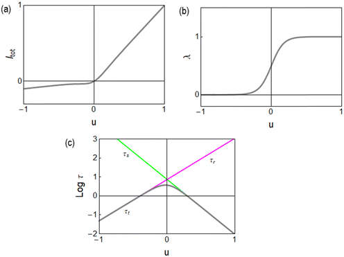 | ||
| Fig. 4 (a) Current–voltage curve. (b) Equilibrium value of the state variable. (c) Relaxation times. Parameters Vs = 0.3, Vr = −0.4, Vm = 0.1, ns = 1.5, nr = 2, gL = 0.1, gH = 1, and τk = 1. | ||
Under a constant voltage sweep at rate vscan
| u = vscant | (13) |
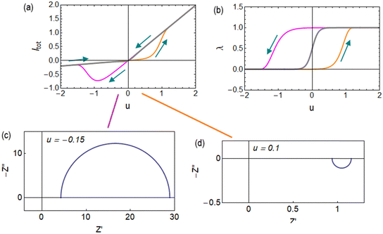 | ||
| Fig. 5 Hysteresis at a rate vscan = 10 in (a) current–voltage curves and (b) state variable. The grey lines are the equilibrium curves. (c) and (d) Impedance spectra at the indicated voltage points. Parameters as in Fig. 4. | ||
To obtain further insight into the dynamical properties of the model, we calculate the small signal ac impedance response at the angular frequency ω. As usual,34,43 the equations are expanded to the first order, where the perturbation of variable y is indicated as ŷ, and the factor functions of each term are computed under equilibrium conditions. Furthermore, we transform the small signal equations to the frequency domain by the Laplace transform, d/dt → s, where s = iω. We obtain the equations
Îtot = [gL + (gH − gL)λ]û + (gH − gL)u![[small klambda, Greek, circumflex]](https://www.rsc.org/images/entities/i_char_e11a.gif) | (14) |
 | (15) |
 | (16) |
 | (17) |
These functions are plotted in Fig. 4c and 6b. The solution of the impedance obtained from 14 and 15 is
 | (18) |
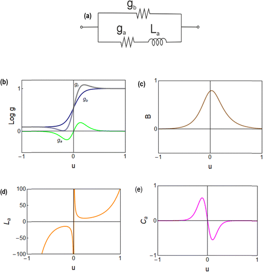 | ||
| Fig. 6 (a) Equivalent circuit. Functions determining the impedance response. (b) Differential conductances, gt = gb + ga. (c) B. (d) Inductor. (e) Effective low frequency capacitance. Parameters as in Fig. 4. | ||
The equivalent circuit corresponding to eqn (18) is shown in Fig. 6a. In this case, the circuit elements are defined by the relationships
| gb = gL + (gH − gL)λ | (19) |
| ga = B(gH − gL)τtu | (20) |
 | (21) |
The behavior of differential conductance is shown in Fig. 6b. The resulting impedance spectra both at positive and negative potentials are shown in Fig. 5c and d. In the set side, the impedance shows an inductor feature, and as it has been explained in many publications, it is associated with the inverted (inductive) hysteresis.22,35 In the negative side, the impedance spectra are purely capacitive, as also observed in the experimental data of Fig. 1. However, the impedance model of eqn (18) and Fig. 6a contains solely an inductor but not a capacitor element. How is the capacitor generated at negative voltages?
To address this question, we calculate the effective capacitance corresponding to the branch (Ra, La) with impedance Za = ga−1 + sLa. This capacitance is given by the expression
 | (22) |
 | (23) |
From (23), if ga > 0, then the system generates the negative capacitance effect that characterizes the chemical inductor.44,47,74–81 However, for ga < 0, the model produces a positive low frequency capacitance. We can see in Fig. 6b that the change of the sign of ga occurs at V = 0, causing the positive capacitance at negative voltages as shown in Fig. 6e. We conclude that the capacitance observed in the reset process originates in the same delayed conduction process as the inductor in the set process.
It is also remarked that the inductor element La in Fig. 6d becomes negative when ga is negative.62 This ensures that the small perturbation relaxation time τt = gaLa is positive at all voltages (as required for a stable system62), as shown in Fig. 4c.
While the model described applies to a variety of systems with specific conduction and memristive mechanisms, it is worthwhile to discuss the expected value of the conduction inductor and conduction capacitance, which have produced doubts of interpretation when measured in some systems, as remarked before.57 Consider a conductance of 1 nA V−1 for a single pore82 or a memristor filament, a kinetic time τk is 1 s. The value of the inductor can be estimated as
 | (24) |
Even if there are 100 conducting units per cm2, as shown in Fig. 1, the conduction inductance can reach a very large value of 107 H cm−2. Obviously, for systems with a short relaxation time, the inductor will be smaller, in the order of μH.46,83 For the conduction capacitance of a single unit in the same example
| Ca = gHτk = 1 nF | (25) |
The conduction capacitance is higher than typical geometric capacitances, but smaller than chemical capacitances.84
In summary, observing large values of inductance and capacitance is good evidence that a memristor has been measured and not an L or a C.
It should be noticed that the use of (7) and (8) predict finite switching times a zero voltage. If required, they can be replaced by expressions in which the switching times become infinite (dλ/dt → 0) at zero voltages. These modifications have been suggested in recent publications;69,70 however, the general mechanism based on eqn (6) for the generation of both capacitance and induction in the ac response should be the same, although with more complex analytical expressions.
The model is very useful to explain other phenomena that have been identified in the research of high-performance halide perovskite solar cells. This is the transition from capacitive to inductive hysteresis, which complicates the assessment of the power conversion efficiency.36,39,85 In this transformation, when the bias voltage increases, the low frequency capacitance becomes an inductor, with the associated transformation of capacitive to inductive hysteresis. This is illustrated in Fig. 7, and the same phenomenon is observed in Fig. 2. The transition has also been remarked in HfO2 resistive RAM memories, as shown in Fig. 3.46 The transition from capacitive to inductive or vice versa as the voltage increases produces a non-zero crossing of the IV curves, which has been recognized well in memristive systems.66,86–88
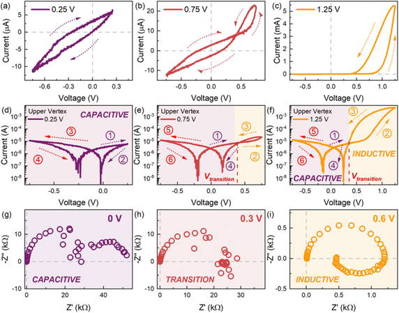 | ||
| Fig. 7 A. Characteristic current–voltage (I–V) response in the linear scale of the halide perovskite memristor device FTO/poly(3,4-ethylenedioxythiophene) polystyrene sulfonate (PEDOT:PSS)/CH3NH3PbBr3/Au with varying upper vertex voltages of (a) 0.25 V, (b) 0.75 V, and (c), 1.25 V, with the arrows indicating the scan direction. The corresponding I–V response in the semi-log scale for upper vertex voltages of (d) 0.25 V, (e) 0.75, and (f) 1.25 V with the arrows and numbers indicating the scan direction and sequence, respectively. Voltage-dependent impedance spectral evolution measured at (g) 0 V, (h) 0.3 V, and (i) 0.6 V exhibiting a transition from a low frequency capacitive response at low applied voltages to a low frequency inductive response at high applied voltages. Figure courtesy of Cedric Gonzales. Reproduced by permission from J. Bisquert, Inductive and capacitive hysteresis of current–voltage curves. A unified structural dynamics in solar energy devices, memristors, ionic transistors and bioelectronics., PRX Energy, 2023, 3, 011001,35 licensed under a Creative Commons Attribution (CC BY 4.0) license. | ||
To analyze the typical evolution of spectra, we add the constant capacitor (3) to the impedance model (18), so that the equivalent circuit of Fig. 8a is obtained. Now, the spectra display two capacitive arcs in the negative voltages, Fig. 8b. The high frequency arc close to the origin corresponds to the geometric capacitance, and the low frequency positive arc corresponds to the conduction capacitance. When approaching the transition voltage, the low frequency arc disappears and becomes an inductor, Fig. 8c, i.e. a negative arc. This is the experimental trend observed in Fig. 1, 2 and 7. This effect has been previously described using different models where the low frequency capacitance is coupled to the memory variable,39,67 as mentioned before. The model of Fig. 8a, based on eqn (6),68 explains well the general tendency of the transformation, with simpler physical components than those considered in previous approaches.
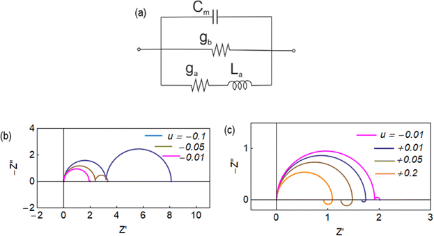 | ||
| Fig. 8 (a) Equivalent circuits and (b) and (c) impedance spectra at different stationary voltages. Same parameters as in Fig. 4 and Cm = 0.001. | ||
In summary, a memristor is described by a set process in which the memory variable λ makes a transition 0 → 1 that promotes the increase of conductance. The associated impedance response is a conduction inductor that becomes quite large in some memristors.43 In the reset cycle, the opposite transition 1 → 0 takes place. We have shown that the impedance feature is a conduction capacitance in this range, and evolves to an inductor in the set range, explaining the transition from capacitive to inductive hysteresis that has been observed in different types of devices. We conjecture that this is a general property of systems with self-crossing hysteresis loops.
Data availability
The data presented here can be accessed at https://doi.org/10.5281/zenodo.10952363 (Zenodo) under the license CC-BY-4.0 (Creative Commons Attribution-ShareAlike 4.0 International).Conflicts of interest
There are no conflicts to declare.Acknowledgements
This work was funded by the European Research Council (ERC) via Horizon Europe Advanced Grant, grant agreement no. 101097688 (“PeroSpiker”). The authors also acknowledge projects PID2022-139586NB-C41 and PID2022-139586NB-C44 funded by MCIN/AEI/10.13039/501100011033 and FEDER, EU.References
- D. V. Christensen, R. Dittmann, B. Linares-Barranco, A. Sebastian and M. Le Gallo, 2022 roadmap on neuromorphic computing and engineering, Neuromorphic Comput. Eng., 2022, 2, 022501 CrossRef.
- J. J. Yang, D. B. Strukov and D. R. Stewart, Memristive devices for computing, Nat. Nanotechnol., 2013, 8, 13–24 CrossRef CAS PubMed.
- Y. Zhang, Z. Wang, J. Zhu, Y. Yang, M. Rao, W. Song, Y. Zhuo, X. Zhang, M. Cui, L. Shen, R. Huang and J. J. Yang, Brain-inspired computing with memristors: Challenges in devices, circuits, and systems, Appl. Phys. Rev., 2020, 7, 011308 CAS.
- J. Zhu, T. Zhang, Y. Yang and R. Huang, A comprehensive review on emerging artificial neuromorphic devices, Appl. Phys. Rev., 2020, 7, 011312 CAS.
- K. Sun, J. Chen and X. Yan, The Future of Memristors: Materials Engineering and Neural Networks, Adv. Func. Mater., 2021, 31, 2006773 CrossRef CAS.
- M. D. Pickett, G. Medeiros-Ribeiro and R. S. Williams, A scalable neuristor built with Mott memristors, Nat. Mater., 2013, 12, 114–117 CrossRef CAS PubMed.
- S. Kumar, X. Wang, J. P. Strachan, Y. Yang and W. D. Lu, Dynamical memristors for higher-complexity neuromorphic computing, Nat. Rev. Mater., 2022, 7, 575–591 CrossRef.
- M. Lanza, A. Sebastian, W. D. Lu, M. Le Gallo, M.-F. Chang, D. Akinwande, F. M. Puglisi, H. N. Alshareef, M. Liu and J. B. Roldan, Memristive technologies for data storage, computation, encryption, and radio-frequency communication, Science, 2022, 376, eabj9979 CrossRef CAS PubMed.
- D. B. Strukov, G. S. Snider, D. R. Stewart and R. S. Williams, The missing memristor found, Nature, 2008, 453, 80–83 CrossRef CAS PubMed.
- L. O. Chua and K. Sung Mo, Memristive devices and systems, Proc. IEEE, 1976, 64, 209–223 Search PubMed.
- L. Chua, Resistance switching memories are memristors, Appl. Phys. A: Mater. Sci. Process., 2011, 102, 765–783 CrossRef CAS.
- Y. V. Pershin and M. Di Ventra, Memory effects in complex materials and nanoscale systems, Adv. Phys., 2011, 60, 145–227 CrossRef.
- J. B. Roldán, E. Miranda, D. Maldonado, A. N. Mikhaylov, N. V. Agudov, A. A. Dubkov, M. N. Koryazhkina, M. B. González, M. A. Villena, S. Poblador, M. Saludes-Tapia, R. Picos, F. Jiménez-Molinos, S. G. Stavrinides, E. Salvador, F. J. Alonso, F. Campabadal, B. Spagnolo, M. Lanza and L. O. Chua, Variability in Resistive Memories, Adv. Intell. Sys., 2023, 5, 2200338 CrossRef.
- H. J. Snaith, A. Abate, J. M. Ball, G. E. Eperon, T. Leijtens, N. K. Noel, S. D. Stranks, J. T.-W. Wang, K. Wojciechowski and W. Zhang, Anomalous Hysteresis in Perovskite Solar Cells, J. Phys. Chem. Lett., 2014, 5, 1511–1515 CrossRef CAS PubMed.
- H.-S. Kim and N.-G. Park, Parameters Affecting I-V Hysteresis of CH3NH3PbI3 Perovskite Solar Cells: Effects of Perovskite Crystal Size and Mesoporous TiO2 Layer, J. Phys. Chem. Lett., 2014, 5, 2927–2934 CrossRef CAS PubMed.
- S. van Reenen, M. Kemerink and H. J. Snaith, Modeling Anomalous Hysteresis in Perovskite Solar Cells, J. Phys. Chem. Lett., 2015, 6, 3808–3814 CrossRef CAS PubMed.
- R. B. Nuernberg, N. M. P. Machado, D. Jouglard, L. D. Campo, M. Malki and M. Neyret, The origin of hysteresis in the electrical behavior of RuO2-glass composite melts, J. Non-Cryst. Solids, 2021, 557, 120596 CrossRef CAS.
- W. Brown, M. Kvetny, R. Yang and G. Wang, Selective Ion Enrichment and Charge Storage through Transport Hysteresis in Conical Nanopipettes, J. Phys. Chem. C, 2022, 126, 10872–10879 CrossRef CAS.
- K. Intonti, E. Faella, L. Viscardi, A. Kumar, O. Durante, F. Giubileo, M. Passacantando, H. T. Lam, K. Anastasiou, M. F. Craciun, S. Russo and A. Di Bartolomeo, Hysteresis and Photoconductivity of Few-Layer ReSe2 Field Effect Transistors Enhanced by Air Pressure, Adv. Electron. Mater., 2023, 9, 2300066 CrossRef CAS.
- R. Shameem, L. M. Bongartz, A. Weissbach, H. Kleemann and K. Leo, Hysteresis in Organic Electrochemical Transistors: Relation to the Electrochemical Properties of the Semiconductor, Appl. Sci., 2023, 13, 5754 CrossRef CAS.
- A. Migliore and A. Nitzan, Irreversibility and Hysteresis in Redox Molecular Conduction Junctions, J. Am. Chem. Soc., 2013, 135, 9420–9432 CrossRef CAS PubMed.
- J. Bisquert and A. Guerrero, Chemical Inductor, J. Am. Chem. Soc., 2022, 144, 5996–6009 CrossRef CAS PubMed.
- A. L. Hodgkin and A. F. Huxley, A quantitative description of membrane current and its application to conduction and excitation in nerve, J. Physiol., 1952, 117, 500–544 CrossRef CAS PubMed.
- M. Häusser, The Hodgkin-Huxley theory of the action potential, Nat. Neurosci., 2000, 3, 1165 CrossRef PubMed.
- H. R. Wilson, Spikes, Decisions, and Actions: The Dynamical Foundations of Neuroscience, Oxford University Press, 1999 Search PubMed.
- A. J. Hopper, H. Beswick-Jones and A. M. Brown, A color-coded graphical guide to the Hodgkin and Huxley papers, Adv. Physio. Edu., 2022, 46, 580–592 CrossRef PubMed.
- Y. Bu, Z. Ahmed and L. Yobas, A nanofluidic memristor based on ion concentration polarization, Analyst, 2019, 144, 7168–7172 RSC.
- D. Wang, W. Brown, Y. Li, M. Kvetny, J. Liu and G. Wang, Hysteresis Charges in the Dynamic Enrichment and Depletion of Ions in Single Conical Nanopores, ChemElectroChem, 2018, 5, 3089–3095 CrossRef CAS.
- P. Ramirez, J. Cervera, S. Nasir, M. Ali, W. Ensinger and S. Mafe, Electrochemical impedance spectroscopy of membranes with nanofluidic conical pores, J. Colloid Interface Sci., 2024, 655, 876–885 CrossRef CAS PubMed.
- A. C. Lazanas and M. I. Prodromidis, Electrochemical Impedance Spectroscopy–A Tutorial, ACS Meas. Sci. Au, 2023, 3, 162–193 CrossRef CAS PubMed.
- M. E. Orazem and B. Tribollet, Electrochemical Impedance Spectroscopy, 2nd edn, Wiley, 2017 Search PubMed.
- V. Vivier and M. E. Orazem, Impedance Analysis of Electrochemical Systems, Chem. Rev., 2022, 122, 11131–11168 CrossRef CAS PubMed.
- A. Bou and J. Bisquert, Impedance spectroscopy dynamics of biological neural elements: from memristors to neurons and synapses, J. Phys. Chem. B, 2021, 125, 9934–9949 CrossRef CAS PubMed.
- J. Bisquert, Current-controlled memristors: resistive switching systems with negative capacitance and inverted hysteresis, Phys. Rev. Appl., 2023, 20, 044022 CrossRef CAS.
- J. Bisquert, Inductive and capacitive hysteresis of current-voltage curves. A unified structural dynamics in solar energy devices, memristors, ionic transistors and bioelectronics., PRX Energy, 2023, 3, 011001 CrossRef.
- J. Bisquert, A. Guerrero and C. Gonzales, Theory of Hysteresis in Halide Perovskites by Integration of the Equivalent Circuit, ACS Phys. Chem. Au, 2021, 1, 25–44 CrossRef CAS PubMed.
- W. Tress, J. P. Correa Baena, M. Saliba, A. Abate and M. Graetzel, Inverted Current–Voltage Hysteresis in Mixed Perovskite Solar Cells: Polarization, Energy Barriers, and Defect Recombination, Adv. Energy Mater., 2016, 6, 1600396 CrossRef.
- V. Lopez-Richard, R. S. Wengenroth Silva, O. Lipan and F. Hartmann, Tuning the conductance topology in solids, J. Appl. Phys., 2023, 133, 134901 CrossRef CAS.
- C. Gonzales, A. Guerrero and J. Bisquert, Transition from capacitive to inductive hysteresis: A neuron-style model to correlate I-V curves to impedances of metal halide perovskites, J. Phys. Chem. C, 2022, 126, 13560–13578 CrossRef CAS.
- N. Filipoiu, A. T. Preda, D.-V. Anghel, R. Patru, R. Elizabeth Brophy, M. Kateb, C. Besleaga, A. Gabriel Tomulescu, I. Pintilie, A. Manolescu and G. Alexandru Nemnes, Capacitive and inductive effects in perovskite solar cells: The different roles of ionic current and ionic charge accumulation, Phys. Rev. Appl, 2022, 18, 064087 CrossRef.
- A. O. Alvarez, R. Arcas, C. A. Aranda, L. Bethencourt, E. Mas-Marzá, M. Saliba and F. Fabregat-Santiago, Negative Capacitance and Inverted Hysteresis: Matching Features in Perovskite Solar Cells, J. Phys. Chem. Lett., 2020, 11, 8417–8423 CrossRef CAS PubMed.
- I. Fernandez-Guillen, C. A. Aranda, P. F. Betancur, M. Vallés-Pelarda, C. Momblona, T. S. Ripolles, R. Abargues and P. P. Boix, Perovskite Thin Single Crystal for a High Performance and Long Endurance Memristor, Adv. Electron. Mater., 2024, 2300475 CrossRef.
- M. Berruet, J. C. Pérez-Martínez, B. Romero, C. Gonzales, A. M. Al-Mayouf, A. Guerrero and J. Bisquert, Physical model for the current-voltage hysteresis and impedance of halide perovskite memristors, ACS Energy Lett., 2022, 7, 1214–1222 CrossRef CAS.
- C. Gonzales, A. Guerrero and J. Bisquert, Spectral properties of the dynamic state transition in metal halide perovskite-based memristor exhibiting negative capacitance, App. Phys. Lett., 2021, 118, 073501 CrossRef CAS.
- M. Maestro-Izquierdo, M. B. Gonzalez, F. Campabadal, J. Suñé and E. Miranda, A New Perspective Towards the Understanding of the Frequency-Dependent Behavior of Memristive Devices, IEEE Electron Device Lett., 2021, 42, 565–568 CAS.
- S. Dueñas, H. Castán, H. García, Ó. G. Ossorio, L. A. Domínguez and E. Miranda, Experimental Observation of Negative Susceptance in HfO2-Based RRAM Devices, IEEE Electron Device Lett., 2017, 38, 1216–1219 Search PubMed.
- I. Mora-Seró, J. Bisquert, F. Fabregat-Santiago, G. Garcia-Belmonte, G. Zoppi, K. Durose, Y. Y. Proskuryakov, I. Oja, A. Belaidi, T. Dittrich, R. Tena-Zaera, A. Katty, C. Lévy-Clement, V. Barrioz and S. J. C. Irvine, Implications of the negative capacitance observed at forward bias in nanocomposite and polycrystalline solar cells, Nano Lett., 2006, 6, 640–650 CrossRef PubMed.
- A. Zohar, N. Kedem, I. Levine, D. Zohar, A. Vilan, D. Ehre, G. Hodes and D. Cahen, Impedance Spectroscopic Indication for Solid State Electrochemical Reaction in (CH3NH3)PbI3 Films, J. Phys. Chem. Lett., 2016, 7, 191–197 CrossRef CAS PubMed.
- H. Dhifaoui, N. H. Hemasiri, W. Aloui, A. Bouazizi, S. Kazim and S. Ahmad, An Approach to Quantify the Negative Capacitance Features in a Triple-Cation based Perovskite Solar Cells, Adv. Mater. Interfaces, 2021, 8, 2101002 CrossRef CAS.
- F. Ebadi, N. Taghavinia, R. Mohammadpour, A. Hagfeldt and W. Tress, Origin of apparent light-enhanced and negative capacitance in perovskite solar cells, Nat. Commun., 2019, 10, 1574 CrossRef PubMed.
- G. Garcia-Belmonte and J. Bisquert, Distinction between Capacitive and Noncapacitive Hysteretic Currents in Operation and Degradation of Perovskite Solar Cells, ACS Energy Lett., 2016, 1, 683–688 CrossRef CAS.
- N. Pebere, C. Riera and F. Dabosi, Investigation of magnesium corrosion in aerated sodium sulfate solution by electrochemical impedance spectroscopy, Electrochim. Acta, 1990, 35, 555–561 CrossRef CAS.
- V. Shkirskiy, A. D. King, O. Gharbi, P. Volovitch, J. R. Scully, K. Ogle and N. Birbilis, Revisiting the Electrochemical Impedance Spectroscopy of Magnesium with Online Inductively Coupled Plasma Atomic Emission Spectroscopy, ChemPhysChem, 2015, 16, 536–539 CrossRef CAS PubMed.
- S. K. Roy, M. E. Orazem and B. Tribollet, Interpretation of Low-Frequency Inductive Loops in PEM Fuel Cells, J. Electrochem. Soc., 2007, 154, B1378 CrossRef CAS.
- I. Pivac, B. Šimić and F. Barbir, Experimental diagnostics and modeling of inductive phenomena at low frequencies in impedance spectra of proton exchange membrane fuel cells, J. Power Sources, 2017, 365, 240–248 CrossRef CAS.
- I. Pivac and F. Barbir, Inductive phenomena at low frequencies in impedance spectra of proton exchange membrane fuel cells – A review, J. Power Sources, 2016, 326, 112–119 CrossRef CAS.
- K. S. Cole, Rectification and inductance in the squid giant axon, J. Gen. Physiol., 1941, 25, 29–51 CrossRef CAS PubMed.
- K. S. Cole, Membranes, Ions and Impulses. A Chapter of Classical Biophysics, University of California Press, 1968 Search PubMed.
- A. Hodgkin, Chance and Design: Reminiscences of Science in Peace and War Illustrated Edition, Cambridge University Press, 1992 Search PubMed.
- L. Chua, V. Sbitnev and H. Kim, Hodgkin–Huxley axon is made of memristors, Int. J. Bifurcat. Chaos, 2012, 22, 1230011 CrossRef.
- L. O. Chua, The Fourth Element, Proc. IEEE, 2012, 100, 1920–1927 Search PubMed.
- J. Bisquert, Negative inductor effects in nonlinear two-dimensional systems. Oscillatory neurons and memristors, Chem. Phys. Rev., 2022, 3, 041305 CrossRef CAS.
- J. Bisquert, Device physics recipe to make spiking neurons, Chem. Phys. Rev., 2023, 4, 031313 CrossRef.
- J. Bisquert, Iontronic Nanopore Model for Artificial Neurons: The Requisites of Spiking, J. Phys. Chem. Lett., 2023, 9027–9033 CrossRef CAS PubMed.
- L. Munoz-Diaz, A. J. Rosa, A. Bou, R. S. Sanchez, B. Romero, R. A. John, M. V. Kovalenko, A. Guerrero and J. Bisquert, Inductive and Capacitive Hysteresis of Halide Perovskite Solar Cells and Memristors Under Illumination, Front. Energy Res., 2022, 10, 914115 CrossRef.
- S. Yarragolla, T. Hemke, F. Jalled, T. Gergs, J. Trieschmann, T. Arul and T. Mussenbrock, Nonlinear behavior of area dependent interface type resistive switching devices, arXiv, 2024, preprint, arXiv:2402.04848[cs.ET] DOI:10.48550/arXiv.2402.04848.
- J. Bisquert, Electrical Charge Coupling Dominates the Hysteresis Effect of Halide Perovskite Devices, J. Phys. Chem. Lett., 2023, 14, 1014–1021 CrossRef CAS PubMed.
- E. Miranda and J. Suñé, Memristive State Equation for Bipolar Resistive Switching Devices Based on a Dynamic Balance Model and Its Equivalent Circuit Representation, IEEE Trans. Nanotechnol., 2020, 19, 837–840 CAS.
- E. Miranda, E. Piros, F. L. Aguirre, T. Kim, P. Schreyer, J. Gehrunger, T. Oster, K. Hofmann, J. Suñé, C. Hochberger and L. Alff, Simulation of Bipolar-Type Resistive Switching Devices Using a Recursive Approach to the Dynamic Memdiode Model, IEEE Electron Device Lett., 2023, 44, 1551–1554 Search PubMed.
- F. L. Aguirre, J. Suñé and E. Miranda, SPICE Implementation of the Dynamic Memdiode Model for Bipolar Resistive Switching Devices, Micromachines, 2022, 13, 330 CrossRef PubMed.
- J. Bisquert, A. Bou, A. Guerrero and E. Hernández-Balaguera, Resistance transient dynamics in switchable perovskite memristors, APL, Mach. Learn., 2023, 1, 036101 Search PubMed.
- J. Cervera, J. A. Manzanares and S. Mafe, Electrical Coupling in Ensembles of Nonexcitable Cells: Modeling the Spatial Map of Single Cell Potentials, J. Phys. Chem. B, 2015, 119, 2968–2978 CrossRef CAS PubMed.
- C. M. Armstrong, Ionic pores, gates, and gating currents, Q. Rev. Biophys., 1974, 7, 179–209 CrossRef CAS PubMed.
- A. K. Jonscher, The physical origin of negative capacitance, J. Chem. Soc., Faraday Trans. 2, 1986, 82, 75–81 RSC.
- M. Ershov, H. C. Liu, L. Li, M. Buchanan, Z. R. Wasilevski and A. K. Jonsher, Negative Capacitance Effect in Semiconductor Devices, IEEE Trans. Electron Devices, 1998, 48, 2196 CrossRef.
- E. Ehrenfreund, C. Lungenschmied, G. Dennler, H. Neugebauer and N. S. Sariciftci, Negative capacitance in organic semiconductor devices: Bipolar injection and charge recombination mechanism, App. Phys. Lett., 2007, 91, 012112 CrossRef.
- J. Bisquert, G. Garcia-Belmonte, A. Pitarch and H. Bolink, Negative capacitance caused by electron injection through interfacial states in organic light-emitting diodes, Chem. Phys. Lett., 2006, 422, 184–191 CrossRef CAS.
- L. S. C. Pingree, B. J. Scott, M. T. Russell, T. J. Marks and M. C. Hersam, Negative capacitance in organic light-emitting diodes, App. Phys. Lett., 2005, 86, 073509 CrossRef.
- F. Fabregat-Santiago, M. Kulbak, A. Zohar, M. Vallés-Pelarda, G. Hodes, D. Cahen and I. Mora-Seró, Deleterious Effect of Negative Capacitance on the Performance of Halide Perovskite Solar Cells, ACS Energy Lett., 2017, 2, 2007–2013 CrossRef CAS.
- D. Klotz, Negative capacitance or inductive loop? – A general assessment of a common low frequency impedance feature, Electrochem. Comm., 2019, 98, 58–62 CrossRef CAS.
- M. T. Khan, P. Huang, A. Almohammedi, S. Kazim and S. Ahmad, Mechanistic origin and unlocking of negative capacitance in perovskites solar cells, iScience, 2021, 24, 102024 CrossRef CAS PubMed.
- D. Wang, M. Kvetny, J. Liu, W. Brown, Y. Li and G. Wang, Transmembrane Potential across Single Conical Nanopores and Resulting Memristive and Memcapacitive Ion Transport, J. Am. Chem. Soc., 2012, 134, 3651–3654 CrossRef CAS PubMed.
- S. Dueñas, H. Castán, K. Kukli, M. Mikkor, K. Kalam, T. Arroval and A. Tamm, Memory Maps: Reading RRAM Devices without Power Consumption, ECS Trans., 2018, 85, 201 CrossRef.
- J. Bisquert, Chemical capacitance of nanostructured semiconductors: its origin and significance for heterogeneous solar cells, Phys. Chem. Chem. Phys., 2003, 5, 5360–5364 RSC.
- E. H. Balaguera and J. Bisquert, Accelerating the Assessment of Hysteresis in Perovskite Solar Cells, ACS Energy Lett., 2024, 9, 478–486 CrossRef PubMed.
- S. Yarragolla; T. Hemke; J. Trieschmann and T. Mussenbrock, Non-zero crossing current-voltage characteristics of interface-type resistive switching devices, 2024, arXiv:2401.14507 [cond-mat.mes-hall].
- B. Sun, M. Xiao, G. Zhou, Z. Ren, Y. N. Zhou and Y. A. Wu, Non–zero-crossing current-voltage hysteresis behavior in memristive system, Mater. Today Adv., 2020, 6, 100056 CrossRef.
- S. Saraf, M. Markovich, T. Vincent, R. Rechter and A. Rothschild, Memory diodes with nonzero crossing, App. Phys. Lett., 2013, 102, 022902 CrossRef.
| This journal is © the Owner Societies 2024 |
