
Light outcoupling strategies in oriented perovskite light-emitting-diodes: recent trends, opportunities, and challenges toward innovation
Muhammad Imran
Saleem
 a,
Rino
Choi
*ab and
Jeong-Hwan
Lee
*ab
a,
Rino
Choi
*ab and
Jeong-Hwan
Lee
*ab
aDepartment of Materials Science and Engineering, Inha University, Incheon 22212, Republic of Korea. E-mail: Rino.Choi@inha.ac.kr; jeong-hwan.lee@inha.ac.kr
b3D Convergence Center, Inha University, Incheon 22212, Republic of Korea
First published on 3rd May 2023
Abstract
Metal halide perovskites (MHPs) exhibit outstanding photophysical properties, such as high photoluminescence quantum yield (PLQY), high exciton binding energy, narrow emission spectrum, tailorable bandgap, and facile solution-processibility. MHPs have opened a scientific revitalization in the light-emitting diode (LED) technology. Tremendous research efforts have been carried out, such as balancing electron–hole injection, modulation of stoichiometric compositions, ligand engineering, and minimal non-radiative recombination that boosted the internal quantum efficiency near unity. However, the lower external quantum efficiency and operational stability of perovskite LEDs (PeLEDs) than organic LEDs make them limited to display and lighting applications. One of the main reasons is the trapped photons inside the devices, which reduces light outcoupling. This review includes a detailed analysis of existing challenges in managing light outcoupling of PeLEDs and discusses various strategies adopted for these challenges. Control of dipole orientations, refractive index matching, oriented quasi-two-dimensional structures, and thickness optimization are existing methodologies to address the improved light outcoupling in PeLEDs. We discuss a detailed prospect for high-performance PeLEDs for practical applications.
1. Introduction
Over the past few decades, tremendous efforts have been devoted to developing new semiconductors with outstanding electronic and optical properties. With the development of materials science combined with innovative device fabrication methodologies, numerous high-performance optoelectronic devices have been developed, including photodetectors,1–6 photovoltaic cells,7–9 light-emitting diodes (LEDs),10–12 and transistors.13–16 The successful realizations of optimized morphologies, including nanostructures, single-crystal wafers, and thin films, have allowed countless optoelectronic devices to meet the end-users prospects.17–20 The low-dimensional semiconducting materials, such as 0D quantum dots, 1D nanowires/nanorods, 2D quantum wells, and 3D hierarchical structures, possess tunable optical and electrical properties. Furthermore, they allow for diverse light-matter interactions as well as high aspect ratios stemming from their unique surface morphology, contrary to bulk counterparts. Notably, the crystallographic orientation among the low-dimensional semiconducting materials is essential as a building block for various optoelectronic devices. The well-defined morphology of oriented nanostructures has the ability for directional charge separation or transfer, and homo-/hetero-junction formation with other semiconductors.21,22 Thus, these properties promote the performance of oriented nanostructures and serve as an effective avenue for the fundamental photophysical exploration of numerous materials.In recent years, the development of well-defined size, shape, and controlled surface morphologies of oriented nanostructures has been successfully realized, and their potential application in high-performance optoelectronic devices has been demonstrated. To this end, metal halide perovskites (MHPs) have emerged as exciting semiconducting materials for next-generation display and lighting applications due to their excellent photophysical properties, tailorable bandgap, and solution-processibility. The general chemical formula of a 3D perovskite structure is ABX3, where A is a monovalent cation (MA, (CH3NH3+), FA, (HCNH2)2+, Cs+), B is a divalent cation, and X is a halide anion (Cl−, Br−, I−). In ABX3 structures, the BX6 structure is formed so that one divalent metal cation is connected to six halide anions, as shown in the 3D structure of MHP (Fig. 1a). Unlike the bulk 3D perovskite, the reduced dimension is low-dimensional, such as quantum dots, 1D nanowires/nanorods, and 2D nanosheets/nanoplatelets (Fig. 1b). These perovskites possess distinctive advantages of quantum-confinement effects and shape diversity.
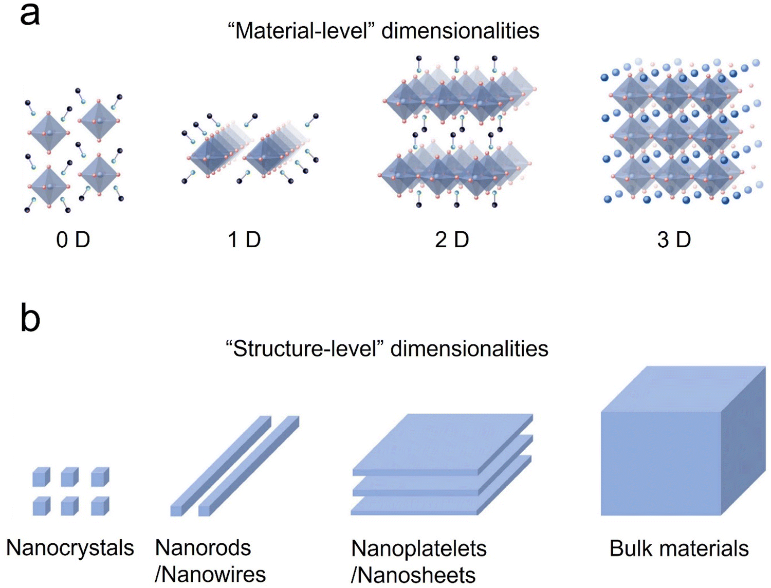 | ||
| Fig. 1 (a and b) Simulated structures and schematic illustration of material-level, structure-level 3D perovskites, and their low-dimensional counterparts, respectively. Reproduced with permission.64 Copyright 2020, Wiley-VCH. | ||
The general chemical formula of mixed quasi-two-dimensional Ruddlesden–Popper (RP) is L2An−1PbnX3n+1, where L (phenyl-ethyl ammonium (PEA), butylammonium (BA)) is a large aromatic or aliphatic alkyl ammonium cation, A is an organic cation, B is a divalent metal cation, X is a halide anion, and n is the number of inorganic layers.23,24 The replacement of bulky organic cations with small organic cations (PEA, BA) resulted in the formation of a quasi-two-dimensional perovskite structure. These quasi-2D layered structures are oriented organic and inorganic layers, and octahedral [BX6]4− inorganic layers are sandwiched by the two layers of PEA, BA counter cations. Thus, naturally occurring quantum wells and multi-bandgap structures that tightly confined excitons within organic layers enhance the photoluminescence quantum yield (PLQY) by suppressing the non-radiative recombination (Fig. 1a and b). The RP quasi-two-dimension perovskite energy level and bandgap can be determined from the dimensionality. Due to quantum confinement effects, the bandgap gradually increases as n number of inorganic layers decreases from ∞ (3D) to 1 (2D). The RP-phased MHPs of n = 1 or 2 are highly efficient for eliminating non-radiative recombination rates, owing to the enhanced electron–hole pair confinement in these phases.
The past five years have witnessed the rapid advancement of MHP by optimizing their optoelectrical properties, including high PLQY, emission color purity, tailorable bandgap, and high charge carrier mobilities to meet the internal quantum efficiency close to unity.5,25–30 The utilization of MHP in optoelectronic devices could eliminate the drawback associated with conventional semiconductors (e.g., organic or Cd/Zn-chalcogenides QDs). For instance, in 2009, the photovoltaic function of MHP with a power conversion efficiency of 3.8% was reported. Soon after this report, it was observed that high PLQY and suppressed defect formation in MHP should be an ideal candidate for luminance devices.7 These properties and low-temperature solution-processibility have propelled the MHP for modern lighting and display technologies.
In 2014, Richard H. Friend's group introduced room-temperature perovskite light-emitting diodes (PeLEDs) with a luminance efficiency of 364 cd m−2 and external quantum efficiency (EQE) below 0.1%.31 This work set a new standard for triggering the fast development of PeLEDs in display applications as they have a distinct advantage over the current main display source, organic LEDs, in terms of the high color purity covering the REC.2020 standard with narrow full-width at half-maximum (FWHM) emission spectra.
Since the pioneering work, immense efforts have been devoted to further improving the performance of PeLEDs, making the EQE close to the value of organic LEDs. Researchers have emulated past breakthroughs to explore numerous oriented perovskite nanostructures to enhance the intrinsic emission characteristics of perovskites. For example, Lee et al. studied the excess of metallic lead (Pb) in perovskite to eliminate the non-radiative recombination rates.32 An optimized amount of Pb in perovskite led to an optimized morphology, such as well-packed nanograins with uniform coverage from scattering micro-sized cuboids. This strategy induced enhanced light outcoupling, leading to a 20![[thin space (1/6-em)]](https://www.rsc.org/images/entities/char_2009.gif) 000-fold efficiency increment in PeLEDs compared with control devices. Xiong et al. reported the colloidal synthesis of MAPbBr3 nanoparticles with a diameter of less than 10 nm.33 These colloidal nanoparticles possessed a high PLQY of over 90%, including large exciton binding energy, which enabled PeLEDs efficiency of 3.8%. Wang et al. reported on multiple quantum wells perovskite with energy-funneling to reduce non-radiative recombination rates associated with defects and leakage current.34 The multiple quantum wells perovskites boosted electroluminescence due to the confinement in lower energy gap quantum wells by higher energy gaps quantum wells, resulting in an improved EQE of over 11%. The EQE of 14.36% was reported based on optimized quasi-two-dimensional perovskites through composition, phase engineering, and surface engineering.35 The EQE of over 20% was obtained with quasi-core shell techniques that effectively passivated non-radiative recombination losses, boosting the PLQY.36 Additionally, an EQE of 28.9% was reported using a simple in situ reaction of benzyl phosphonic acid additive with three-dimensional (3D) polycrystalline perovskite films.37Fig. 2 shows the yearly progress of green, infrared, sky-blue, and blue PeLEDs, with the highest value of green PeLEDs now at more than 28.9% (average = 25.2 ± 1.6%), approaching the theoretical limit of isotopically orientated perovskites emitters.37–63
000-fold efficiency increment in PeLEDs compared with control devices. Xiong et al. reported the colloidal synthesis of MAPbBr3 nanoparticles with a diameter of less than 10 nm.33 These colloidal nanoparticles possessed a high PLQY of over 90%, including large exciton binding energy, which enabled PeLEDs efficiency of 3.8%. Wang et al. reported on multiple quantum wells perovskite with energy-funneling to reduce non-radiative recombination rates associated with defects and leakage current.34 The multiple quantum wells perovskites boosted electroluminescence due to the confinement in lower energy gap quantum wells by higher energy gaps quantum wells, resulting in an improved EQE of over 11%. The EQE of 14.36% was reported based on optimized quasi-two-dimensional perovskites through composition, phase engineering, and surface engineering.35 The EQE of over 20% was obtained with quasi-core shell techniques that effectively passivated non-radiative recombination losses, boosting the PLQY.36 Additionally, an EQE of 28.9% was reported using a simple in situ reaction of benzyl phosphonic acid additive with three-dimensional (3D) polycrystalline perovskite films.37Fig. 2 shows the yearly progress of green, infrared, sky-blue, and blue PeLEDs, with the highest value of green PeLEDs now at more than 28.9% (average = 25.2 ± 1.6%), approaching the theoretical limit of isotopically orientated perovskites emitters.37–63
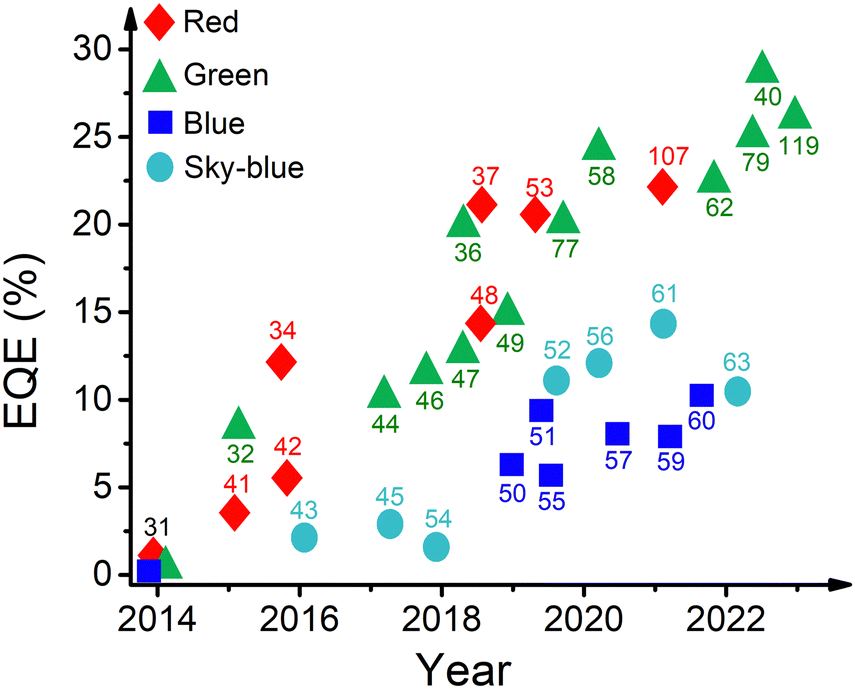 | ||
| Fig. 2 The recent progress of red (diamonds), green (triangles), blue (squares), and sky-blue (circles) PeLEDs. The numbers correspond to their respective reference numbers. | ||
Although PeLEDs have shown significant progress in enhancing the EQE, their EQE value still lags behind that of OLEDs, which is currently close to 40%. The difference in EQE between PeLEDs and OLEDs stems from the disparity in the outcoupling efficiency assuming that IQE is nearly unity. For further enhancement in EQEs of PeLEDs, it is essential to manage light outcoupling. When considering the device structure of PeLEDs compared to organic LEDs, the difference is only the emitting layer since the other layers are almost similar in the two cases. However, despite the encouraging efforts that have been made for balancing electron–hole injection, modulation of stoichiometric compositions, ligand engineering, and minimal non-radiative recombination, the outcoupling management of PeLEDs has scarcely been explored compared to that of organic LEDs. Therefore, this review focuses on recent advancements in oriented perovskite nanostructures of their application in PeLEDs to improve the outcoupling efficiency. Notably, this review is targeted at giving a complete overview of the oriented growth of perovskites along the specific direction to enhance the light extraction efficiency of PeLEDs. The high horizontal dipole ratios of the anisotropic perovskite emitter, the divergence of refractive indices, the photon-recycling process, and film thickness for outcoupling efficiency improvement have been discussed in detail.
2. Light-outcoupling in perovskite light-emitting diodes
The EQE (ηEQE) of PeLEDs is a function of the internal quantum efficiency (ηIQE) and outcoupling efficiency (ηout), and can be expressed with eqn (1):| ηEQE = ηIQE × ηout = fbalance × fe−h × ηradiative × ηout | (1) |
The ηout of PeLEDs typically depends on parameters such as the angle of emissive transition dipole moments (TDMs) in-plane or out-of-plane with the substrate surface, film thickness, photon-recycling process, and refractive indices of the consisting layer. In PeLEDs, the outcoupling efficiency losses are ascribed to a series of optical modes, such as waveguide mode, surface plasmon polaritons, substrate mode, and intrinsic absorption mode.74 The waveguide mode is mainly owing to the discrepancy between the refractive index of the vertically stacked consisting layers in the device that confined more than 20% of the generated photons.75 Additionally, the surface plasmon polaritons mode (20–30%), absorption mode (<10%), and substrate mode (10–30%) dissipate the different portions of generated light within the device.76,77 Namely, the refractive index (n) gap between the active layers and the ambient medium severely hampered the ηout. According to classic ray optics, the n of the randomly oriented TDM-based active layers and ηout are related by ηout = 1/2n2. For perovskite emissive layers typically having n of 2.0–2.6, the ηout is limited to 15%, which severally reduces the ηEQE of PeLEDs.78,79
Film thickness is another influencing factor to ηout. The optimized film thickness of EML and Indium tin oxide (ITO) layers significantly impacts the density of trapped light within the waveguide and substrate mode. The theoretical results reveal that 40% of generated light can be outcoupled with the optimized thickness of ITO and EML layers.80,81 Additionally, the photon recycling process is an important parameter to understand the outcoupling efficiency of PeLEDs beyond the predicted value of classical ray-optics theory.
For the details, we will discuss the extraction of internally trapped electroluminescence, with the oriented growth of perovskites, template-assisted, pattern-nanophononics-assisted growth, oriented TDMs, and refractive indices matching. Film thickness optimization and the photon recycling process's role in enhancing outcoupling are also presented in this review. This review comprises numerous research efforts developed to extract generated photons from the device.
2.1. Refractive indices matching
Owing to the complex photonic process in perovskites EML, the efficiency gap between the state-of-art organic LEDs and PeLEDs is quite high. The predominant reason is the high index of the perovskite emissive layer (n > 2.2) relative to the ambient medium (n = 1), leading to the induction of enormous optical losses, unlike OLEDs having n ≈ 1.7–1.8 for transporting layers and EML. The refractive index mismatching in the perovskite multilayered structure gives rise to modifying the outcoupling angle. If the angle is very small, the generated photons in the EML are hardly extracted. Thus, reducing the EML index increases the outcoupling angle and thus has the potential to increase the outcoupling efficiency. However, the enhanced outcoupling does not always make the brightness boost. For the brightness, we only count the number of photons emitted close to a normal angle to the surface of the substrate (in-between 0° and less than 3° angles). However, for outcoupling, one counts the photon flux from all angles. Thus, after the refractive index modification, photons at a higher angle likely contribute to enhancing outcoupling, rather than the ones at the normal 0° angle, which are already extracted out even in the devices without the modification of n. To simultaneously enhance the outcoupling and brightness, other strategies should be combined to change the path of the photons at a high angle when extracted. Here, we will focus on the outcoupling enhancement via refractive index modification.As shown in the previous literature, the effective management of refractive indices of consisting layers in PeLEDs is one of the crucial determinants to enhancing the outcoupling efficiency.78,79 The ηout corresponds to the fraction of light escaping from the PeLED stack, deducting from the interfacial total-internal-reflection and Purcell-effect losses.82 The C.-J. Shih group reported on the FA0.5MA0.5PbBr3 nanocrystals capped with alkylamine amphiphiles with different hydrophobic tail groups to control the ligand hydrophobicity.83 The alkylamine amphiphiles capped FA0.5MA0.5PbBr3 nanocrystals possess effective n values of 1.64–1.75 (Fig. 3a), corresponding to a maximum ηout of 26%, the maximum luminance of 3322 cd m−2 and ηext of 9.01% based on the FA0.5MA0.5PbBr3 nanocrystals PeLED (Fig. 3b and c). Hassan et al. synthesized MAPb(IxBr1−x)3 nanocrystals employing a modified ligand-assisted re-precipitation method.84 The n ∼ 1.82 (620 nm), ηout (32.2%), and ηext of 20% were estimated from the MAPb(IxBr1−x)3 nanocrystals-LEDs.
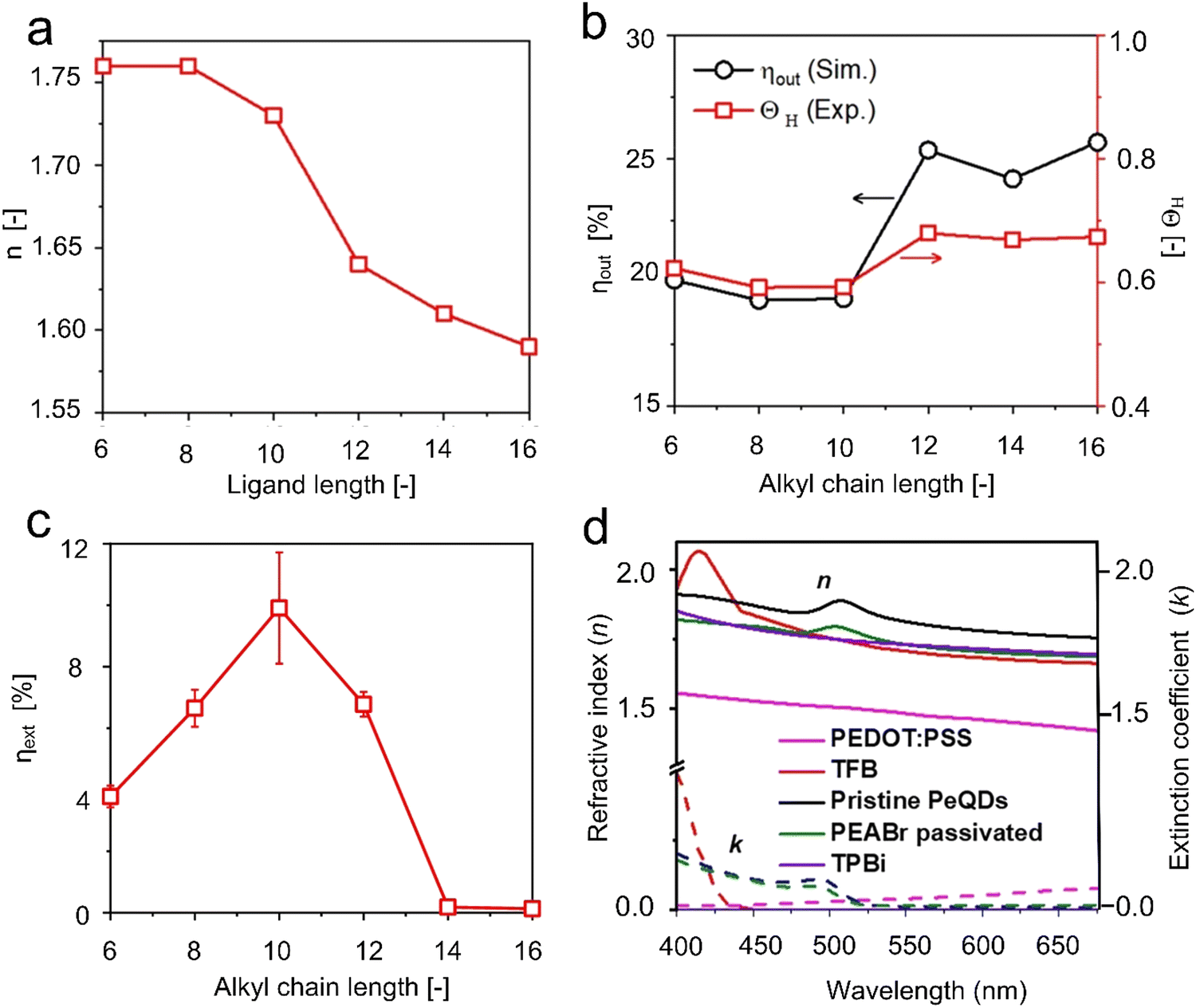 | ||
| Fig. 3 (a) The n profile of FA0.5MA0.5PbBr3 perovskite nanocrystals capped with alkylamine ligands varying the alkyl chain length. (b) Extracted probability of horizontal transition dipole moments (ΘH) and calculated light outcoupling efficiency, ηout, as a function of alkyl chain length, and (c) ηext distribution as a function of the alkyl chain.83 Copyright 2019, American Chemical Society. (d) Refractive indices (n) and extinction coefficients (k) of the PEDOT:PSS, TFB, pristine CsPbBr3, phenylethyl ammonium-passivated CsPbBr3, and TPBi in PeLED as a function of wavelength. Reproduced with permission.75 Copyright 2021, Elsevier. | ||
Additionally, He et al. reported that the effectiveness of the organic cation ligand exchange is an attractive approach to lower the large contrast n of the transporting layer and perovskite EML.75 The pristine CsPbBr3 and passivated films exhibit n values of 1.91 and 1.82 at 520 nm, respectively. The lower n value in the passivated film indicates the coupling associated with the ligand exchange. Consequently, an efficiency enhancement was reported from 1.0% to 6.85% and luminance from 1300 cd m−2 to 13000 cd m−2 for the control and passivated CsPbBr3 PeLEDs, respectively. The improved performance of phenylethyl ammonium-CsPbBr3 passivated PeLEDs was attributed to enhanced light-outcoupling efficiency owing to the reduced n value (Fig. 3d). Subsequently, the n of the perovskite emissive layer can be adjusted by using a pre-deposited thin layer of poly(2-hydroxyethyl methacrylate), pHEMA.76 The refractive index of pHEMA is around 1.9 (calculated at the peak of its steady-state luminescence), and halide perovskite is n ∼ 2.7, and this discrepancy of n value significantly trapped the generated light of more than 70%. The pre-deposited thin layer of pHEMA before the ensemble of the perovskite film helped to suit the n (∼2.1) values. It extended the escape cone of photon emission from the bulk heterojunction perovskite emissive layer to an angle of 32°, leading to an efficiency of up to 20.1%, with operation stability of T50 = 46 h in the air at peak external quantum efficiency. The theoretical analysis also revealed that an outcoupling enhancement factor of up to 25% could be obtained from the modified EML.
In addition, several nanophotonics/nanopatterns strategies were implemented to enhance the outcoupling efficiency by overcoming the refractive index mismatch. For example, the utilization of rational nanostructures assists in adapting the refractive index matching within devices. Zhang et al. introduced 3D anodic alumina membranes-based nanophotonic substrate.85 By properly controlling the refractive index, the substrate with a nanowire array optical antenna layer acts as a nano-dome array light coupler (Fig. 4a). Therefore, the generated light can easily propagate through the anodic alumina membrane (TiO2 nanowires) layer in the vertical direction with reduced light trapping inside the device. For the optimization of the outcoupling, they claimed that the barrier layer nano-domes and TiO2 nanowires array embedded in anodic alumina membrane nanophotonic with pitch size of 1000 nm is more beneficial than a planner and without TiO2 nanowires nano-domes anodic alumina membrane devices. It originates from the core index matching between the TiO2 (n = 2.7) and perovskites (n = 2.6) to form a waveguide to support guided modes coupled from perovskite layers. This nanophotonic structure with nano-domes light couplers and nanowire optical antennas leads to a light extraction efficiency of over 73%, an external efficiency of more than 17%, and a luminance of 48668 cd m−2 at 4 V. Despite the high light extraction efficiency (73%) in this configuration, the low internal quantum efficiency of the emitter makes EQE low (17%). It can be inferred that the EQE of PeLEDs can overcome 30% if we combine a high IQE emitter with this technology.
 | ||
| Fig. 4 (a) Schematic illustration of the vertical TiO2 nanowires-based LED device. Cathode/F8/perovskite/PEDOT:PSS/ITO/anodic alumina membrane filled with TiO2 nanowires array. Reproduced with permission.85 Copyright 2019, Nature Publishing Group. (b) Device structures of PeLEDs with and without nanohole arrays. Reproduced with permission.86 Copyright 2019, Wiley-VCH. (c) Graphic representation of the fabrication process of PeLED with the imprinted nanostructures. Reproduced with permission.87 Copyright 2019, Wiley-VCH. (d) The fabrication process of the nanowires PeLEDs. Reproduced with permission.88 Copyright 2020, American Chemical Society. | ||
Jeon et al. have explored the potential of a nanophotonic structure composed of a randomly distributed nanohole array with a high-index contrast that facilitates light extraction efficiency.86 The randomly distributed nanohole array voids with a 300 nm depth in the SiN layer are propitious for light extraction due to the high n contrast between SiN and the void (Fig. 4b). The finite-difference time-domain simulation results demonstrate that without a randomly distributed nanohole array nanophotonic structure, 87% of the generated light is trapped within the device owing to the divergence of refractive indices between the perovskite emitter and glass substrate. However, randomly distributed nanohole array-embedded PeLEDs provide additional opportunities for light outcoupling enhancement, so a 1.46-times higher efficiency was obtained from this nanohole array structure. More importantly, the near-infrared perovskite LEDs reached a brightness of 16.5 W sr−1 m−2 without the randomly distributed nanohole array nanophotonic structure and 23.7 W sr−1 m−2 with the randomly distributed nanohole array nanophotonic structure. Thus, improved outcoupling in PeLEDs was acquired by employing a nanohole array composed of SiN with embedded voids.
These approaches have enabled the significant reduction of the density of trapped light within the PeLEDs, leading to substantial outcoupling improvement. Furthermore, Shen et al. explored an economical method to effectively eliminate the optical losses associated with the waveguide mode by embedding imprinted bioinspired moth-eye nanostructures at the perovskites anode interface (Fig. 4c).87 The trapping of photons within the waveguide mode had been significantly lessened with the moth-eye nanostructure technique. Subsequently, moth-eye nanostructure-based PeLEDs retained 1.5-times higher performance than flat devices owing to the improvement associated with the efficient outcoupling of the waveguided light.
The directional growth of perovskite nanostructures allows us to achieve enhanced light outcoupling in PeLEDs by activating the radiative and directional emission with better stability provided by the nanostructures-patterned template with the high-index grading of perovskite. Thus, the directional growth of the emissive layer offers an additional benefit of improving the photon management, high-index matching, and superior stability, contrary to planner devices. For example, the growth of the methylammonium bromide (MABr)-modified CsPbBr3 nanophotonic wire LEDs in a porous alumina membrane has been explored with the capillary-effect-assisted solution method (Fig. 4d).88 The efficiency and stability of template-assisted nanophotonic wire-based PeLEDs were increased to 1.45 and 3.89 times compared to the planner device, respectively, owing to the 4 to 5 times (44–51%) increase in the light extraction coefficient of the nanophotonic wire PeLEDs, compared with a light extraction coefficient of the planner device (10%). Additionally, the nanophotonic wire-based PeLEDs can give a luminance of 12016 cd m−2 at 5.5 V, and the planner device only gives 10953 cd m−2 at the same voltage. Thus, the maximum luminance was enhanced by 9.7%, owing to the better light extraction coefficient of the nanophotonic wire.
2.2. Control the orientation of perovskite thin film
The directional growth of nanostructured materials would be advantageous for LED technology, owing to the control of light outcoupling by eliminating the drawback associated with optical trapping within the thin film layers of ITO, a hole-transporting layer, and EML. Subsequently, enormous research efforts have been reported to discover the optoelectronic properties and stability of directional nanostructural materials, including pattern 1D nanophotonic, submicrometer-scale structures, nanorods, nanowires, and quasi-2D perovskites-based LEDs.20,89–93 Among them, strong dielectric- and quantum-confinement effects owing to the large exciton binding energy with quantum well nature and high PLQY of 2D perovskites have emerged as sensational contenders for LED technologies. Even though the internal efficiency of 0D and 3D PeLEDs is equal to unity, an EQE beyond 20% is hardly achievable due to limited outcoupling. Conversely, the EQE of 2D PeLEDs can achieve over 25%, enabled by the anisotropic emitter outstripping the intrinsic light outcoupling limit in PeLEDs.79To realize anisotropic light emission, it is crucial to orient the TDM, a vector quantity associated with the direction of the electronic oscillation between the ground and emissive elements of emitting materials. In general, TDMs that are horizontally oriented with respect to the substrate are favored for light outcoupling, while vertically oriented TDMs largely contribute to energy loss in vertically stacked architectures.94 In this way, horizontally oriented TDMs with the crystal facing parallel to the substrate surface induce more light extraction from the substrate by reducing the guided and substrate modes, which can compensate for the refractive mismatching issue.
The angular dependence PL spectra and back focal plane imaging were investigated to quantify the orientation of TDMs. The experimental setup for obtaining the angle-dependent PL consists of a mounted glass slide with a thin layer of nanoplate film onto a half-cylindrical prism (Fig. 5a). The intensity of the emitted photons is measured per an angle after exciting the film with the appropriate power and wavelength of the laser source. The emitting light from this experiment is used in conjunction with the 1D microcavity model.95 This model effectively estimates the anisotropy of the emitting materials and provides information on the alignment constant (ζ).96 The value of the alignment constant (ζ = 0, 1) is bound between zero and one for horizontally and vertically aligned TDMs with the ensemble film, respectively. The alignment constant, the refractive index, and the angle of the emissive TDM to the film substrate is given by eqn (2):
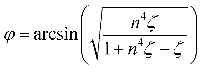 | (2) |
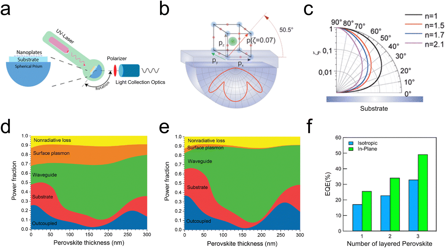 | ||
| Fig. 5 (a) Measurement setup for angle-dependent PL. Reproduced with permission.97 Copyright 2019, American Chemical Society. (b) The value of the alignment constant determined the angle of the transition dipole moment vector. (c) The value of the alignment constant (ζ), and the refractive indices dependent profile. Reproduced with permission.96 Copyright 2017, American Chemical Society. (d and e) Power distribution into different optical modes of PeLEDs with various perovskite layer thicknesses for (d) isotropic dipole orientation (Θ = 0.33) and (e) horizontal dipole orientation (Θ = 0). Reproduced with permission.98 Copyright 2020, The Optical Society. (f) Simulated in-plane or out-of-plane oriented TDMs distribution versus efficiency for PeLEDs. The n represents layered perovskites quantum-wells. Reproduced with permission.99 Copyright 2020, American Chemical Society. | ||
The anisotropic emitter has raised the efficiency of LEDs by more than 40%, owing to high horizontal-to-vertical dipole ratios. Cui et al. reported that 84% horizontally oriented TDMs are expected from ensemble perovskite nanoplates and yield 31% outcoupling efficiency (anisotropic film), which is higher than that from the isotropic emitter (∼23%).94 The large portion of horizontally oriented TDMs boosted the EQE of LEDs to 23.6% and a maximum brightness of 3140 cd m−2. Additionally, by carefully optimizing the horizontally oriented TDMs, the LEDs efficiency could be increased to the upper level of ∼40%.94
Kumar et al. reported that controlling the aspect ratio of the anisotropic nanocrystal superlattices perovskite emitter is essential to enhance the light outcoupling in PeLEDs.79 They claimed that, for a given dipole, the emission radiative rate is the product of the transition dipole moment (p) and local electric field (f) vectors, i.e., (p·f)2. Under the assumption of the isotropic TDM orientation, ΘIP is given by eqn (3),
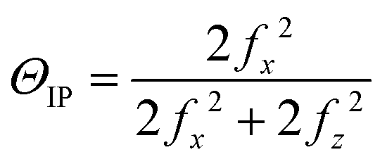 | (3) |
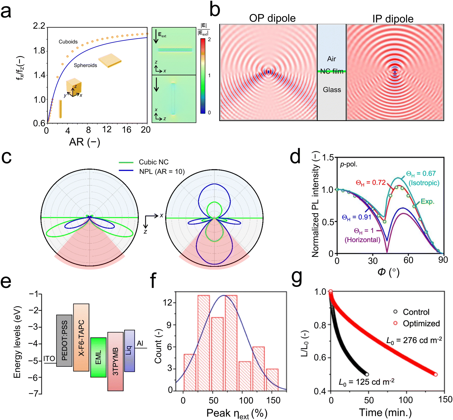 | ||
| Fig. 6 (a) Calculated ratio of horizontal (x) to vertical (z) local field factor, fx/fz, as a function of the aspect ratio. Calculated electric field intensity profiles (b) and radiation patterns (c) in the x–z plane for an out-of-plane (OP; left) and in-plane (IP; right). (d) Angle-dependent PL. (e) Schematic illustration of PeLEDs, and (f and g) optoelectronic properties of PeLEDs. Reproduced with Permission.79 Copyright 2022, Nature Publishing Group. | ||
2.3. Control of crystallinity of perovskite layer
The outcoupling efficiency of PeLEDs can be manipulated with the control of the crystallinity of the perovskite EML, as a high crystalline thin film also induces a preferentially oriented emission.100 In addition, the highly crystalline perovskite thin film has uniform surface morphology, reduced defects, and a well-organized, orderly packed surface, which can avoid nonradiative decay and induce efficient light emission. In recent years, strategies using additive and template-assisted growth have been explored to improve the crystallinity of perovskite EML, including metal halides, organic molecules, and ammonium halides.101–106:1 (x: PAM, PAC) was spin-coated and heated at 100 °C for 20 min for 3D FAPbI3 thin film formation. The surface morphology analysis of the additive-assisted (pentane-1-amine and pentanoic acid) method reveals that the perovskite layer is well-connected and has a regular-shaped grain, contrary to the control film. Significantly, the faceted shape of the crystallites was obtained using a pentane-1-amine-based additive. Regular and large grain perovskite grains become more regular, owing to a strong hydrogen bond network (PAM + FA + I [FA + I]n)+ (Fig. 7a stage I). The low purity of FA+ and PAM+ additive acts as a template for the vertical growth of perovskite due to standing order along the interface between the perovskite and air, boosting the continuous vertical growth of the pentane-1-amine-based perovskite crystal (Fig. 7a stage II). After the intermediate (stage II), the annealing process results in well-organized in-plane growth of a perovskite crystal (stage III). On the other hand, it was observed that the weak interaction between pentanoic acid and FA led to earlier crystal growth and randomly oriented perovskites (Fig. 7b, stage I–III). The optoelectronic properties of the PeLEDs (ITO/polyethylenimine ethoxylated (PEIE)-ZnO/EML/TFB/MoOx/Au; 60 nm) based on pentane-1-amine- and pentanoic acid-additive were investigated. The efficiency of 14.2 ± 0.9 and 12.5 ± 1.2% and half-lifetime (T50) of 9.5 and 5.4 h for pentane-1-amine- and pentanoic acid-additive were realized, respectively. It was noticed that for the discrete crystallinity of 3D FAPbI3 with multifunctional groups, 2-(2-(2-aminoethoxy)ethoxy)acetic acid-additives, the outcoupling efficiency could be improved to 29.1 ± 2.4%. A radiance of 250 W sr−1 m−2 and peak efficiency of over 22.2% were also reported with 2-(2-(2-aminoethoxy)ethoxy)acetic acid-additives assisted growth.
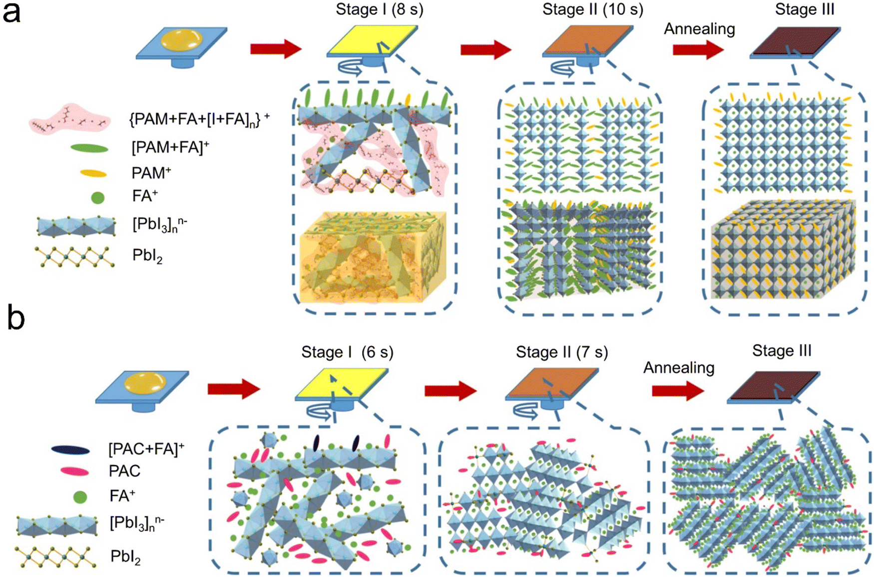 | ||
| Fig. 7 (a) Pentane-1-amine-assisted oriented growth. (b) Isotropic growth with pentanoic acid additive. Reproduced with permission.107 Copyright 2021, Nature Publishing Group. | ||
Additionally, Cao et al. successfully showed effective electroluminescence from solution-processed perovskites that have a tendency to form submicrometre-scale structures by introducing amino-acid additives (Fig. 8a).38 The formation of the discrete submicrometre-structure perovskite involves faceted platelets with roughly rectangular shapes. The platelets are randomly tiled on the substrate, and the size of the platelets is between 100 nm and 500 nm (Fig. 8b). As shown in Fig. 8a, the wide-angle light (ray A) can enter the low-index organic layer and propagate into the glass substrate. The 3D finite-difference-time-domain (3D-FDTD) simulations were further carried out to analyze the outcoupling efficiency in the 3D perovskite film and submicrometre platelets. The results show that a 3D perovskite device with a continuous and flat emitting layer has an outcoupling efficiency of 21.8%. Surprisingly, the outcoupling efficiency of a device with submicrometre-structures reaches about 30%.
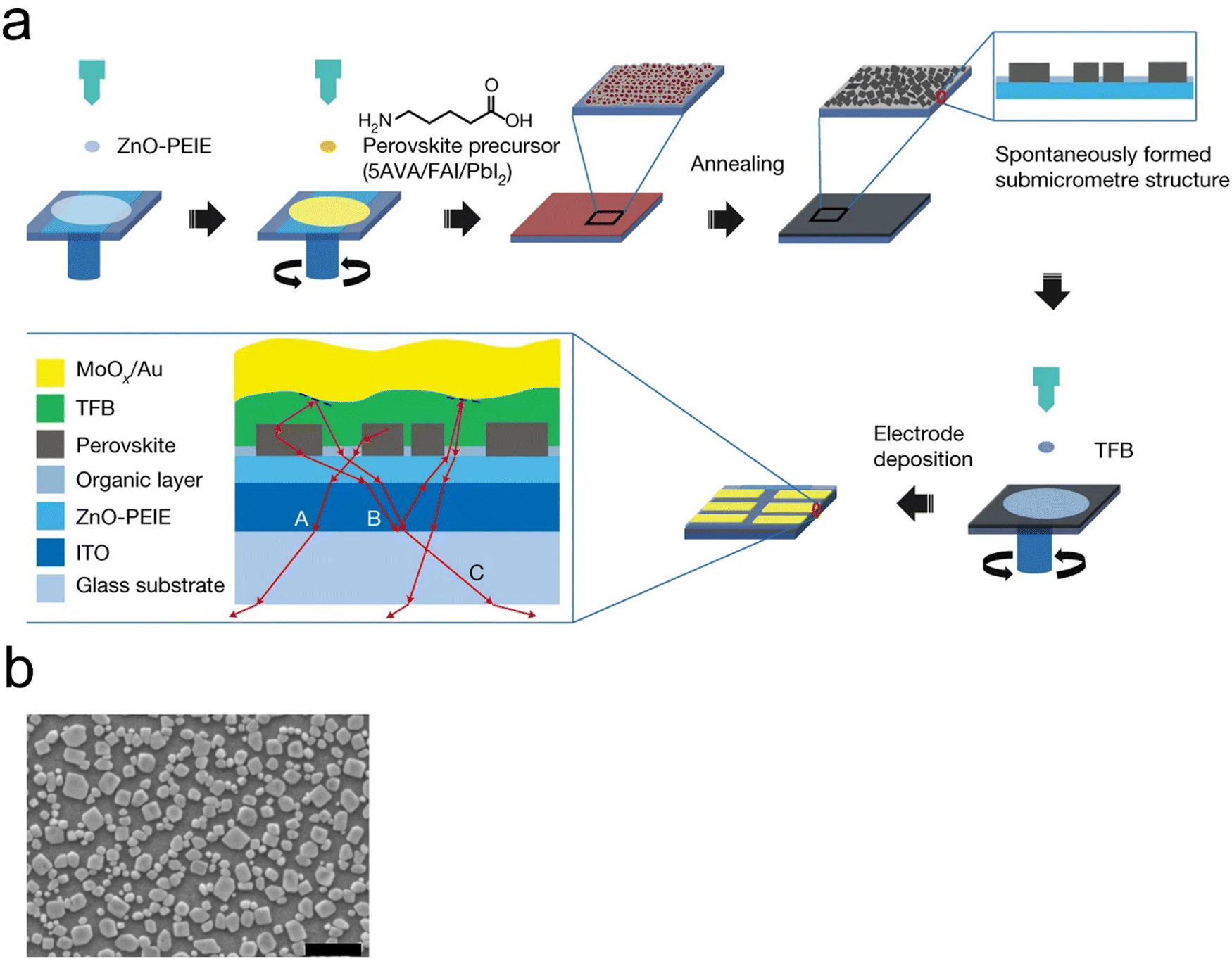 | ||
| Fig. 8 (a) Fabrication of the device and formation of the submicrometre-structure. Rays A, B and C, representing light trapped in devices with a continuous emitting layer, can be extracted by the submicrometre-structure. (b) SEM image of the submicrometre perovskite. Reproduced with permission.38 Copyright 2018, Nature Publishing Group. | ||
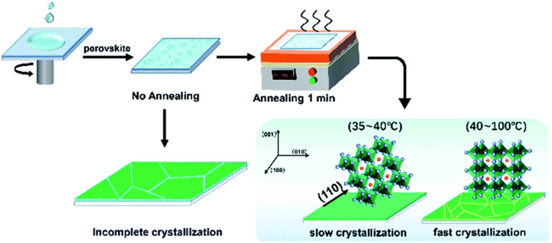
Furthermore, the crystal orientation is essential for the high-quality perovskite 3D film, which reduces the surface defect density and increases the surface coverage owing to well-organized packed crystals.108 As schematically illustrated in Fig. 9, the temperature range between 35–40 °C was considered an ideal value for preferential orientation along the (110) crystal plane, and to avoid the fast crystallization process associated with the solution-processed 3D perovskite film. The translated PeLEDs of this highly oriented perovskite film exhibit a high brightness of 79932 cd m−2, external efficiency of 16.45%, and T50 of 136 h at an initial luminance of 100 cd m−2. Thus, crystal orientation along the (110) crystal plane and uniform surface coverage in the temperature range of 35–40 °C is an exciting way to manipulate the fast-crystallization process to enhance the PeLEDs performance.
 | ||
| Fig. 9 Schematic illustration of the oriented growth of the perovskite with slow (35–40 °C) and fast (40–100 °C) crystallization strategy. Reproduced with permission.108 Copyright 2021, Royal Society of Chemistry. | ||
It was recently noticed that the hydrophobicity of the glass substrate had impeded the highly crystalline growth in the perovskite film.109 Lowering the hydrophobic nature of the bottom layer or glass substrate is necessary to realize crystalline perovskite film growth. There have been numerous reports on the nature of the bottom layer. For example, Xiao et al. reported a highly uniform, ultra-flat perovskite film on the plasma-etched hole transporting layer.110 The fabricated PeLEDs delivered a high brightness of 1200 cd m−2, EQE of 10.4%, and significantly improved the shelf operation stability in a controlled environment. It should be noted that the optimized time for plasma etching is 2–6 s. Beyond this limit, the surface of HTL could become damaged, resulting in deteriorated electronic properties.111
Additionally, the in situ grown thickness-controlled quantum-well CsPbBr3 on a thin layer of poly(9-vinyl carbazole) (PVK) growth template was also reported.112 This template facilitated the low trap densities, high PLQY, and well-defined surface morphology and oriented crystal along the [020] planes parallel to the substrate surface, resulting in high-color-purity PeLEDs with a full width at a half maximum (FWHM) of 82 meV, yielding a maximum brightness of ∼14000 cd m−2 at 8 V with external efficiency exceeded from 10.4%. However, such growth templates hamper the device fabrication's reliability owing to the solubility of PVK in N,N-dimethylformamide (DMF), and dimethylsulfoxide (DMSO) leads to the mixing of PVK with perovskite. To avoid the above issue, a thin layer of polymer (polyvinylpyrrolidone, PVP) coating on the HTL may allow for protection and prevent the intermixing of HTL with the perovskite film. Thus, Kong et al. addressed an approach to accomplish the energy transfer pathway in perovskite films using methanesulfonate on a pre-deposited thin layer of PVP growth template.113 The quasi-2D perovskite is reconstructed owing to methanesulfonate interaction with the spacer butylammonium cations via strong hydrogen bonding, which raises the energy acceptor-to-donor ratios and increases the energy transfer in perovskite films. Their approach leads to a current efficiency of 63 cd A−1, a peak luminance of 13400 cd m−2 at a low applied voltage of 5.5 V, and 20.5% external quantum efficiency.
Although such a high efficiency was reported, the solvent selection for PVP and HTL should be unique. Otherwise, intermixing of PVP and HTL could occur, which would deteriorate the bottom layers. Another strategy to eradicate the issues mentioned above was reported for the formation of high-quality perovskite films via the application of a thermally evaporated ultrathin layer (1 nm) of lithium fluoride (LiF) growth template.69 This growth template enabled the formation of high-quality perovskite films aligned parallel to the substrate normal (i.e., preferred oriented along the [020] planes to the substrate surface). Hence, the oriented perovskite films exhibit a PLQY of 65%, and an efficiency of 19.1% with ultrahigh brightness of over 1500 cd m−2 was reported from PeLEDs.69 The tedious fabrication of 1 nm LiF in an ultrahigh vacuum is a major stumbling block.
The oriented perovskite film enables a high outcoupling and a high-color purity with a narrow emission spectrum, which is anticipated to apprehend a wide color gamut in high-resolution displays. The highly aligned three-dimensional MAPbBr3 film in the [001] direction can be obtained from a quasi-two-dimension perovskite growth template composed of phenylethylammonium lead bromide (PEA2PbBr4).114 The reference 3D bulk and 2D films are scattered with large separated cubic crystals (Fig. 10a, stage I–II). Contrary to their counterparts, the ion exchange conversion of 2D into a 3D MAPBr3 film appeared to be closely placed plate-like crystallites (Fig. 10a, stage III). Notably, the reduced crystallographic defect density and well-organized oriented film resulted in ultranarrow electroluminescence spectra with an FWHM of 15.3 nm and color purity of 98.1% among the reported organic-inorganic green PeLEDs. Transient optical outcoupling experiments predicted that the excitons are dissociated into electron–hole significantly at lower-energy states within ∼1 ps. The observed ultrafast transition of excitations limits the possibility of non-radiative recombination rates, promoting radiative emission through a bimolecular channel, leading to the efficiency of up to 20.1%, highest luminance of 945 cd m−2 with operation stability of T50 = 46 h in the air at peak EQE.
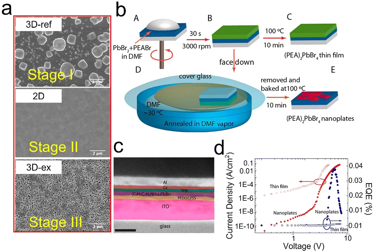 | ||
| Fig. 10 (a) Scanning electron microscopy (SEM) image of the 3D reference (stage I), 2D (stage II), and converted 3D film from the 2D template (stage III). Reproduced with permission.114 Copyright 2018, American Chemical Society. (b) Synthesis of (PEA)2PbBr4 thin films and nanoplates on PEDOT:PSS-coated ITO substrates. (A and B) A DMF solution of 2:1 2-phenylethylammonium bromide and PbBr2 is spin-coated onto a PEDOT:PSS (blue)-coated ITO substrate (gray). The spin-coated film was either directly baked at 100 °C for 10 min to prepare polycrystalline (PEA)2PbBr4 thin films (C), or annealed in DMF vapor (D) and then baked at 100 °C for 10 min to prepare (E) micrometer-sized (PEA)2PbBr4 nanoplates (purple). (c and d) Cross-sectional SEM image and J–V dependence (red symbols) and EQEs (blue symbols) for LEDs. Reproduced with permission.115 Copyright 2016, American Chemical Society. | ||
The interaction of small organic cations such as 2-phenylethylammonium with 3D polycrystalline film transformed the 3D into 2D layered perovskite films.115 During the process, the implementation of solvent vapor annealing resulted in well-organized oriented micrometer-sized nanoplatelets (Fig. 10b). The emergence of (00l) peaks in surface analysis strengthens the understanding of the out-of-plane orientation of quasi-two-dimensional perovskites. These well-organized oriented nanoplatelets-based 2D layered perovskites not only enhance the crystallinity, but the photophysical properties are also improved. PeLEDs showed low subthreshold leakage currents and significantly high efficiency, demonstrating a pure violet emission (Fig. 10c and d).115
2.4. Film thickness
The outcoupling efficiency can be managed by the thickness of the perovskite emissive layer and bottom transparent conductive ITO anode. The EML and ITO thickness significantly impact the density of trapped light within optical modes (waveguide and substrate mode) owing to the divergence of refractive indices. The waveguide loss in PeLEDs configuration is substantial due to high n values. Thus, the optimized thickness of the EML can effectively suppress waveguiding and improve light outcoupling. For example, 9 nm thick ensemble perovskite nanoplates yielded a 31% outcoupling efficiency and PeLEDs efficiency of more than 23.6%.94 Additionally, by carefully optimizing the optical constant and film thickness, external efficiency could be increased to the upper level of ∼40%.Zhao et al. reported that the optimized thickness of EML is 35–50 nm to acquire the efficiency of 17.6% for 40 nm Cs0.2FA0.8PbI2.8Br0.2, 14.3% for 35 nm MAPbI3, 10.1% for 40 nm FAPbI3, and 11.3% for 50 nm FAPbBr3-based PeLEDs (Fig. 11a–e).81 The optical simulations were performed to understand the primary origin of the improved EQE using a thinner perovskite emitting layer (Fig. 11f). The simulation results further verify the experimental observations, and the optimal outcoupling efficiency occurs with perovskite thicknesses in the range of 35–40 nm, where the waveguide mode loss is minimized. Jung et al. also analyzed the efficiency and thickness characteristics to compensate for the high n value of ITO and EML.116 The optical simulation reveals that an efficiency of 25% could be achieved with an identical thickness of both ITO and perovskite emissive layer (∼20 nm). However, achieving stable electrical conductivity and reproducibility with 20 nm thick ITO is challenging. Thus, a 200 nm thick ITO layer and 30 nm perovskite EML with an obtained EQE of 21% were used to lower the density of trapped light within the substrate and waveguide modes.
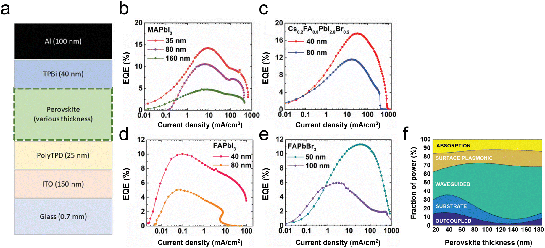 | ||
| Fig. 11 (a) Device configuration of PeLEDs. (b–e) The efficiency and current density curves of EML with different thicknesses. The optimized thickness of EML is 35–50 nm to acquire the efficiency of 17.6% for 40 nm Cs0.2FA0.8PbI2.8Br0.2, 14.3% for 35 nm MAPbI3, 10.1% for 40 nm FAPbI3, and 11.3% for 50 nm FAPbBr3-based PeLEDs. (f) Optical power distribution analysis versus perovskite emitting layer thickness PeLEDs. Reproduced with permission.81 Wiley-VCH. | ||
More importantly, the outcoupling efficiency can be increased by further thinning the emissive layer by about 10 nm.117 The thin emissive layer reduces the refractive index of the functional layers, essentially decreasing the fraction of light trapped in the waveguide modes. This ultra-thin regime enables the enhancement of the EQE to over ∼30% without the need for a complex photonic structure, as illustrated in Fig. 12. They performed the theoretical investigation by employing an ITO-coated (thickness 150 nm) glass anode coated with poly(3,4-ethylenedioxythiophene):polystyrene (PEDOT:PSS, 20 nm)/poly(bis(4-phenyl)(2,4,6-trimethylphenyl)amine) (PTAA, 20 nm) hole injection/transport layers and 2,2′,2′′-(1,3,5-benzinetriyl)-tris (1-phenyl-1-H-benzimidazole) (TPBi) (45 nm) electron transport layer covered with a LiF/Al (1 and 100 nm respectively) cathode. Notably, the simulation results in Fig. 12b shows that for a 35–60 nm thick emissive layer, the maximum attainable EQE reaches ∼21–22%. On the other hand, reducing the emissive layer to close to 10 nm ultimately enables one to boost the EQE to over ∼30%. By thinning the emissive layer, there will be a significant reduction in the amount of light trapped in the waveguiding mode due to the decreased effective refractive index of the functional layers (Fig. 12d).
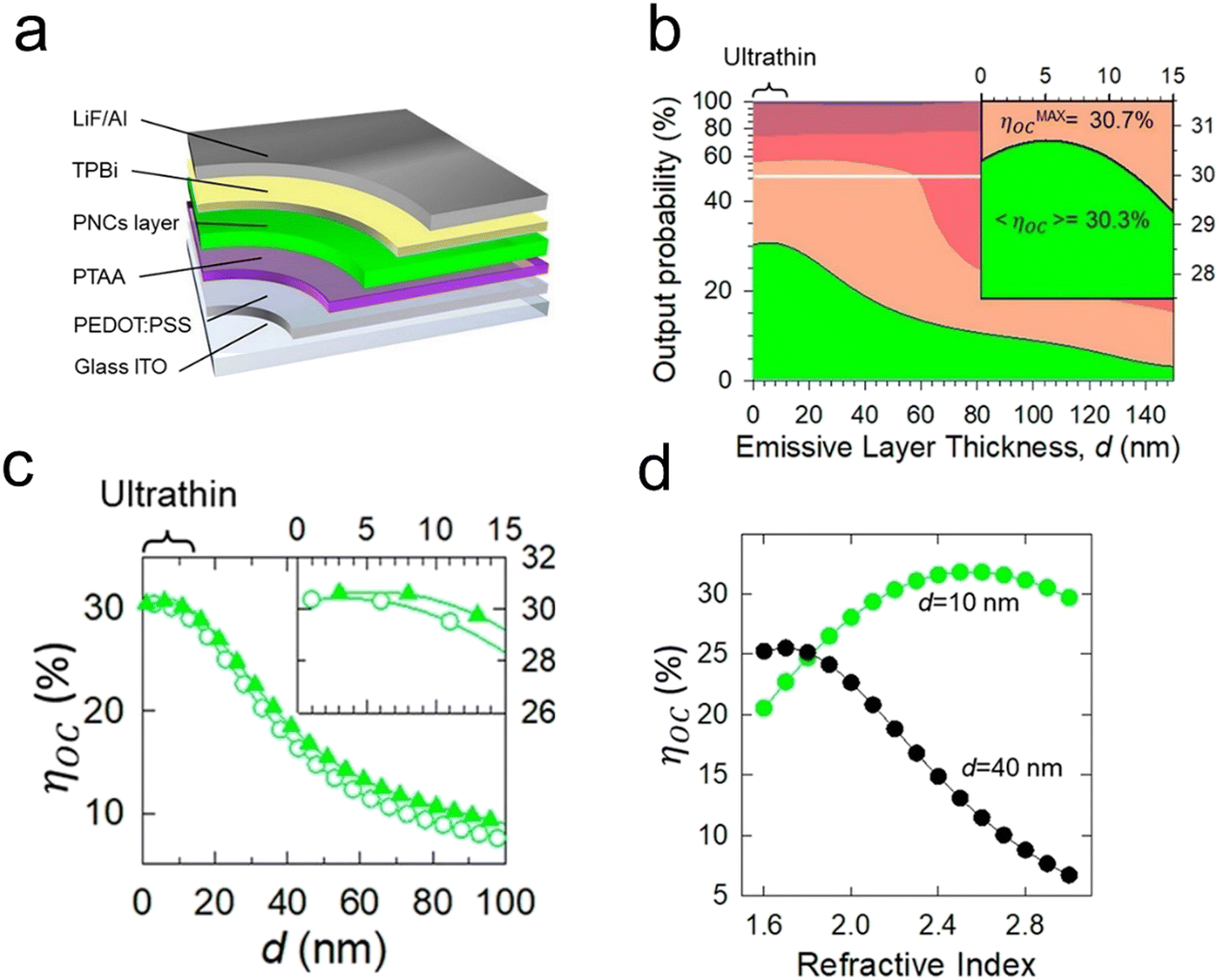 | ||
| Fig. 12 (a) Schematic depiction of PeLEDs with the architecture used for the light outcoupling simulation. (b) Outcoupling probability distribution as a function of the thickness of the emissive layer, thickness (d), for PeLEDs with the same structure as in panel a. The output probability depends strongly on the refractive index and thickness of all functional layers. (c) Comparison between outcoupling (ηOC)-values vs. thickness computed by considering (triangles) or excluding (circles) photon recycling effects. (d) ηOC as a function of the refractive index of ultrathin (d = 10 nm, green circle) and standard (d = 40 nm, black circles) active layer thickness. Reproduced with permission.117 Copyright 2023, American Chemical Society. | ||
2.5 Photon re-absorption in a thick perovskite layer
The efficiency of PeLEDs has surpassed the limit of 30% EQE, despite the high discrepancy of refractive indices (n ≈ 2.0–2.6) and isotopically oriented perovskites emissive layer being surprisingly above the threshold level, which the classical ray-optics theory for outcoupling predicts (7–13%).78 This higher efficiency beyond the expected value shall be probed with a photon-recycling process that significantly increases the outcoupling efficiency of trapped light between different optical modes (waveguide and substrate mode) with sequential re-absorption and re-emission of photons at high radiation efficiency. Notably, a thick perovskite layer dominates this effect. The exceptionality of the photon-recycling process remains distinctive in perovskites owing to the small Stokes shift, which contributes 70% to the overall emission.80 Recent reports show that the outcoupling efficiency can be triggered with the photon-recycling process by re-absorption and re-emission events for given excitations to tailor the photon management from trapped to outcoupling mode.65 Moreover, quantitative analysis showed that an efficiency of 30–50% can be achieved through reduced refractive indices, materials engineering, re-absorption, and effectively eliminating the parasitic absorption through transparent conductive electrodes. Additionally, an efficiency of over 90% is also attainable because of the suppression of parasitic absorption and maximize the photon-recycling effect with an improved device configuration (Fig. 13a and b). Recently, Zhengguo et al. revealed that the thickness-dependent photon-recycling process in a thin film and PeLED device occurs.80 The photon-recycling zone in the entire PeLED device is wider owing to the isotropic random EL emission, contrary to the thin film that is confined in an angle of 38.7° (θglass) (Fig. 13c). The photon-recycling contribution in 30 nm and 2200 nm thick EML is 0.6–2.4% and 40.4%, respectively (Fig. 13d and e). The theoretical analysis shows that all photons are recycled more than once on average before they are outcoupled. The extraordinarily thick (2200 nm) perovskite EML PeLEDs acquired an efficiency of 15.3% owing to the photon-recycling process. Recently, T.-W. Lee's group reported a simple method to produce in situ-formed core/shell nanocrystals by reacting 3D perovskite films with benzyl phosphonic acid.37 The benzyl phosphonic acid treatment separates the 3D perovskites (205 ± 97 nm) to form core/shell perovskite nanocrystals (10 ± 2 nm) (Fig. 14a–c). The trap density was significantly reduced, and the radiative recombination efficiency was substantially enhanced. The 270 nm thick in situ core/shell EML PeLEDs showed a maximum EQE of 28.9%, luminance of 470000 cd m−2, and half-lifetime of 520 h at an initial brightness of 1000 cd m−2. Additionally, optical simulation verified that PeLEDs could reach an EQE of 29.2% with the photon-recycling effect (Fig. 14d).
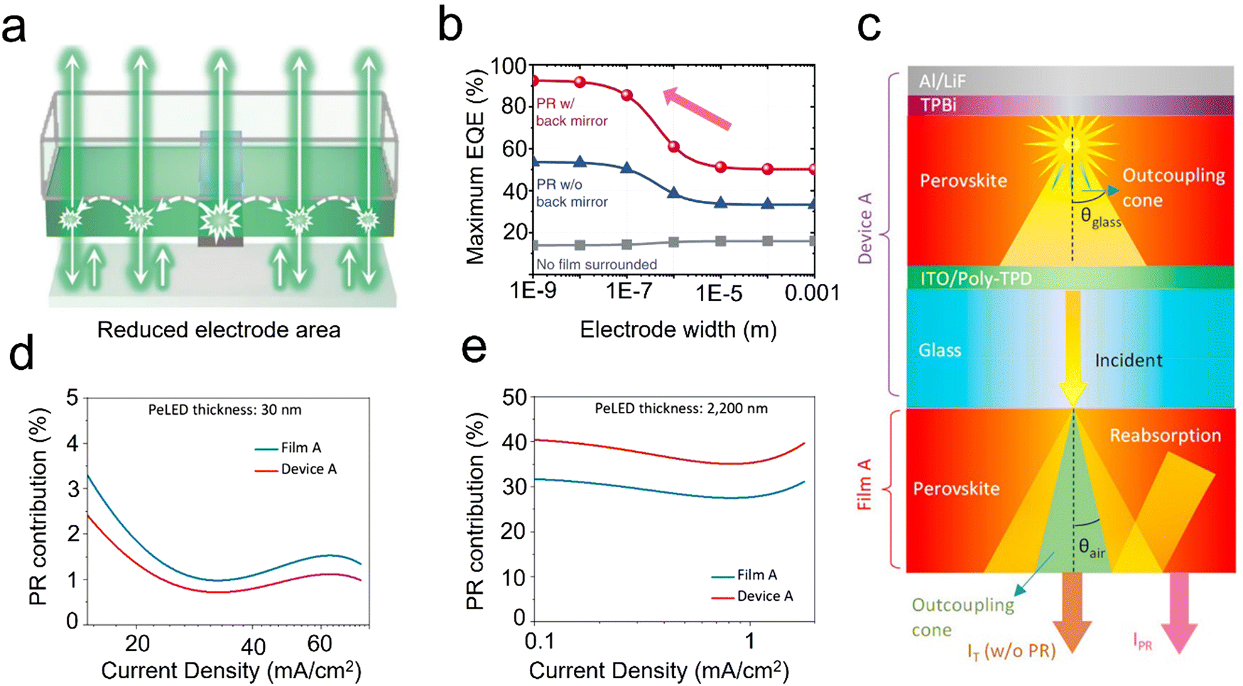 | ||
| Fig. 13 (a) A proposed LED architecture consists of small area electrodes and a large area film, with a reflecting mirror at the bottom. (b) Calculated maximum EQE (IQE = 100%) as a function of the electrode width in the proposed systems having photon-recycling with a back mirror, photon-recycling without a back mirror (only front re-emission is collected), and no film surrounded (photon-recycling only occurs inside the pixel). Reproduced with permission.78 Copyright 2020, Nature Publishing Group. (c–e) Schematic diagram of the photon-recycling zone difference in device A and film A. (d and e) Photon-recycling contribution in film A and real PeLEDs (device A) with a thickness of 30 nm (d) and 2200 nm (e). Reproduced with permission.80 Copyright 2021, American Chemical Society. | ||
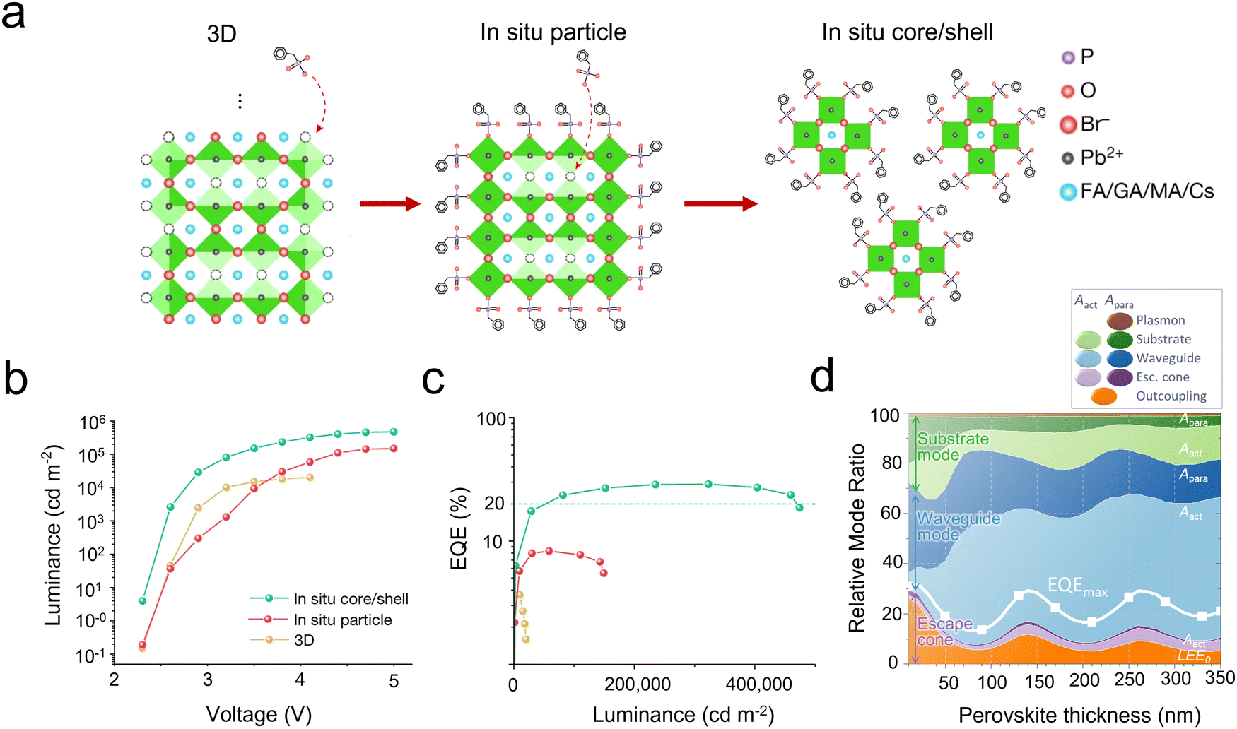 | ||
| Fig. 14 (a) Schematic illustration of the transformation process of 3D (left) into in situ particles (middle) and situ core/shell (right) structures by benzyl phosphonic acid treatment. FA, formamidinium; GA, guanidinium; MA, methylammonium. (b and c) Luminance versus voltage and EQE versus luminance curves of PeLEDs. (d) Calculated maximum EQE considering the effect of photon-recycling as a function of perovskite thickness. Background colors represent the fractions of outcoupling, waveguide, substrate, and plasmon modes per each condition. Non-outcoupled photons are re-absorbed by either perovskite (Aact) or parasitic layers (Apara). Reproduced with permission.37 Copyright 2022, Nature Publishing Group. | ||
Consequently, Richard H. Friend, Dawei Di, Felix Deschler, and Neil C. Greenham discussed78 (a) how ray-optics limits can be suppressed to obtain an efficiency above 20%; (b) what internal quantum efficiency and light extraction efficiencies are being secured in current planar PeLEDs; and (c) how to estimate the upper-efficiency limit of current PeLEDs devices that can be answered owing to the photon-recycling process.
3. Future perspectives
In this review, we have primarily summarized the recent developments in light extraction management in PeLEDs based on theoretical and experimental analyses. Although the abundant strategies, including surface passivation, ligand engineering, cation/anion mixing, and utilizing the efficient energy funneling of 2D layered structure perovskites, have advanced the internal quantum efficiency to more than 90%, an EQE beyond the 20% limit and operational stability owing to a large portion of photon trapping within the thin layer of PeLEDs stack remains and impedes further advancements. Undoubtedly, the remarkable properties of perovskites, including the high PLQY, narrow emission peak, small Stokes Shift, and facile synthesis at a lower temperature, encourage the development of high-performance PeLEDs, which is an inevitable trend of practical applications. Nevertheless, the low operational stability, isotopically oriented emitters, refractive indices discrepancy, and high non-radiative losses owing to poor film coverage and thickness are the few detrimental factors limiting the outcoupling efficiency. Based on the existing literature, we have reviewed the outcoupling management in pattern-nanostructures photonics (quantum wires), vertically oriented quasi-2D perovskites, high-index grading, and anisotropically oriented nanoplatelet emitters (high horizontal dipole ratios of more than 76%). Finally, we have postulated a few strategies for outcoupling efficiency management by examining the photon-recycling process and thickness management in ITO and EML.The anisotropic emitter has raised the modern OLED efficiency by more than 40% due to the high horizontal-to-vertical dipole ratios. Due to the high density of outcoupled photons, the anisotropic emitter with in-plane TDMs would be advantageous for PeLEDs. Sargent et al. quantified the directional emissions from 2D perovskites and revealed that in single crystals, transition dipoles are oriented in-plane (>90). The trade-off between the film thickness and emission anisotropy decreases as the nominal layer thickness increases. Further, theoretical analysis shows that the PeLEDs efficiency of 45% can be obtained from a 2D perovskite (n = 3) owing to a reduction in the surface plasmon modes at the cathode interface, which is excited only by transverse magnetic (TM) polarizations and in emission into waveguided modes.99 The outcoupling efficiency of more than 31% was reported from a monolayer of face-on oriented nine nm thick nanoplatelets. The high horizontal dipole ratio is 84% from an in situ-grown perovskite film, leading to an external quantum efficiency of 23.6%.94 The horizontal dipole ratio of 75% was reported from colloidal anisotropic nanocrystals. The thin film of colloidal anisotropic nanocrystals exhibited a theoretical outcoupling efficiency of 30%, and the 30 nm thick EML demonstrated an external efficiency of 24.96%. All the above strategies have demonstrated emission anisotropy from thin EML layers and photon extraction management.
The divergence of refractive index between the electron-injecting layer, EML, hole-injecting layer, and substrate subsequently leads to optical losses owing to different optical modes such as waveguide mode, substrate mode, and evanescent mode. The discrepancy of refractive indices in state-of-art-LEDs technologies is not very apparent (n ≈ 1.8 for transporting layers and EML). Few reports have been pertinent to overwhelming the trapping of light within LED structures, such as rational design nanostructures, high index-grading, ligand engineering, pre-deposit polymer-assisted method, and moth-eye nanostructures. For example, effective outcoupling management can be obtained by eliminating the optical losses associated with the waveguide mode by embedding an imprinted bioinspired moth-eye nanostructure at the perovskites anode interface.87 The 3D anodic alumina membranes and randomly distributed nanohole array nanophotonic substrates were also explored for outcoupling management. These approaches have enabled the significant reduction of the density of trapped electroluminescence within the PeLEDs devices, leading to efficient outcoupling improvement and enhanced quantum efficiency.85,86
More importantly, thinning the emissive layer can increase the outcoupling efficiency. The thin emissive layer reduces the refractive index of functional layers, essentially decreasing the fraction of light trapped in the waveguide modes. This ultra-thin regime enhances the EQE to over ∼30% without needing a complex photonic structure.
Vertically oriented 2D perovskites have emerged as contenders for optoelectronic devices due to strong dielectric- and quantum-confinement effects owing to large exciton binding energy with quantum well nature and high PLQY. Additionally, the graded energy structures in quasi-2D perovskites are an efficient method for successfully manipulating radiative recombination rates, pattern-nanostructures, and submicrometre-size perovskite crystals have played an essential role in outcoupling management.118 Moreover, the outcoupling efficiency of PeLEDs can be manipulated with the crystallinity of the perovskite EML layer. The highly crystalline perovskite EML layer has uniform surface morphology, reduced defects, and a well-organized, orderly packed surface, leading to adequate device performance.100
A complete understanding of EML and ITO thickness is also necessary. It has been shown that an extraction efficiency of 21% could be achieved with an ITO and EML thickness of ∼200 nm and ∼30 nm, respectively. The efficiency of PeLEDs over the 20% limit, despite the high discrepancy of refractive indices (n ≈ 2.0–2.6) and isotopically oriented perovskites emissive layer (vertically oriented TDMs), is surprisingly above the threshold level, which the classical ray-optics theory for outcoupling predicts (7–13%).78 This efficiency limit beyond the predicted value shall be probed with a photon-recycling process that significantly increases the outcoupling efficiency of trapped light between different optical modes (waveguide and substrate mode) with sequential re-absorption and re-emission of photons at high radiation efficiency. The exceptionality of the photon-recycling process remains distinctive in perovskites owing to the small Stokes shift, which contributes 70% to the overall emission.80
We have noticed that photon-recycling, high horizontal dipole ratios, vertically oriented 2D perovskites, and pattern nanophotonics have resulted in photon extraction management. Anisotropic nanocrystal superlattices with a high horizontal dipole ratio of >85% could achieve more than 30% EQE owing to the high photon out-coupling efficiency. By effectively employing the TDMs, operational stability can also be improved.79 Precise theoretical works are required to encompass oriented TDM ratios, photon-recycling process, and film thickness to further enhance the photon extraction process. Of course, this procedure requires years to mature. This review on oriented PeLEDs outcoupling efficiency management could provide a feasible stance for the future development of anisotropic emitters for practical applications.
4. Conclusions
In this review, we have primarily summarized the recent developments in light extraction management in PeLEDs based on theoretical and experimental analysis. The abundant strategies, including surface passivation, ligand engineering, cation/anion mixing, and utilizing the efficient energy funneling of 2D layered structure perovskites, have advanced the internal quantum efficiency more than 90%. However, the EQE beyond the 20% limit and operational stability, owing to a large portion of photon trapping within the thin layer of PeLEDs stack, remain and impede further advancements. Undoubtedly, the remarkable properties of perovskites, including the high PLQY, narrow emission peak, small Stokes shift, and facile synthesis at a lower temperature, are an encouragement to develop high-performance PeLEDs, which is an inevitable trend of practical applications. Nevertheless, the low operational stability, isotopically oriented emitters, refractive indices discrepancy, and high non-radiative losses owing to poor film coverage and thickness are the few detrimental factors limiting the outcoupling efficiency. Based on existing literature, we have reviewed the outcoupling management in pattern-nanostructures photonics (quantum wires), vertically oriented quasi-2D perovskites, high-index grading, and anisotropically oriented nanoplatelet emitters (high horizontal dipole ratios of more than 76%). Finally, we have postulated a few strategies for outcoupling efficiency management by examining the photon-recycling process and thickness management in ITO and EML.Conflicts of interest
There are no conflicts to declare.Acknowledgements
This research was supported by the Basic Science Research Program through the National Research Foundation of Korea (NRF) funded by the Ministry of Education (2022R1A6A1A03051705). This work was also supported by an Inha University Research Grant (No. 65380-1).References
- K. J. Lee, R. Wei, Y. Wang, J. Zhang, W. Kong, S. K. Chamoli, T. Huang, W. Yu, M. ElKabbash and C. Guo, Gigantic suppression of recombination rate in 3D lead-halide perovskites for enhanced photodetector performance, Nat. Photonics, 2023, 17(4), 236–243 CrossRef CAS.
- F. H. L. Koppens, T. Mueller, P. Avouris, A. C. Ferrari, M. S. Vitiello and M. Polini, Photodetectors based on graphene, other two-dimensional materials and hybrid systems, Nat. Nanotechnol., 2014, 9, 780–793 CrossRef CAS PubMed.
- F. Guo, B. Yang, Y. Yuan, Z. Xiao, Q. Dong, Y. Bi and J. Huang, A nanocomposite ultraviolet photodetector based on interfacial trap-controlled charge injection, Nat. Nanotechnol., 2020, 7, 798–802 CrossRef PubMed.
- R. Saran and R. J. Curry, Lead sulphide nanocrystal photodetector technologies, Nat. Photonics, 2016, 10, 81–92 CrossRef CAS.
- G. Konstantatos and E. H. Sargent, Nanostructured materials for photon detection, Nat. Nanotechnol., 2010, 5, 391–400 CrossRef CAS PubMed.
- L. Dou, Y. Yang, J. You, Z. Hong, W.-H. Chang, G. Li and Y. Yang, Solution-processed hybrid perovskite photodetectors with high detectivity, Nat. Commun., 2014, 6, 5404 CrossRef PubMed.
- A. Kojima, K. Teshima, Y. Shirai and T. Miyasaka, Organometal Halide Perovskites as Visible-Light Sensitizers for Photovoltaic Cells, J. Am. Chem. Soc., 2009, 131, 6050–6051 CrossRef CAS PubMed.
- M. Jeong, W. Choi In, M. Go Eun, Y. Cho, M. Kim, B. Lee, S. Jeong, Y. Jo, W. Choi Hye, J. Lee, J.-H. Bae, K. Kwak Sang, S. Kim Dong and C. Yang, Stable perovskite solar cells with efficiency exceeding 24.8% and 0.3-V voltage loss, Science, 2020, 369, 1615–1620 CrossRef CAS PubMed.
- T. G. Allen, J. Bullock, X. Yang, A. Javey and S. De Wolf, Passivating contacts for crystalline silicon solar cells, Nat. Energy, 2019, 4, 914–928 CrossRef CAS.
- T.-L. Wu, M.-J. Huang, C.-C. Lin, P.-Y. Huang, T.-Y. Chou, R.-W. Chen-Cheng, H.-W. Lin, R.-S. Liu and C.-H. Cheng, Diboron compound-based organic light-emitting diodes with high efficiency and reduced efficiency roll-off, Nat. Photonics, 2018, 12, 235–240 CrossRef CAS.
- Y. Yang, Y. Zheng, W. Cao, A. Titov, J. Hyvonen, J. R. Manders, J. Xue, P. H. Holloway and L. Qian, High-efficiency light-emitting devices based on quantum dots with tailored nanostructures, Nat. Photonics, 2015, 9, 259–266 CrossRef CAS.
- C.-S. Jo, K. Noh, S. H. Noh, H. Yoo, Y. Kim, J. Jang, H. H. Lee, Y.-J. Jung, J.-H. Lee, J. Han, J. Lim and S.-Y. Cho, Solution-Processed Fabrication of Light-Emitting Diodes Using CsPbBr3 Perovskite Nanocrystals, ACS Appl. Nano Mater., 2020, 3, 11801–11810 CrossRef CAS.
- J.-H. Lee, T.-H. Ke, J. Genoe, P. Heremans and C. Rolin, Overlapping-Gate Organic Light-Emitting Transistors, Adv. Electron. Mater., 2019, 5, 1800437 CrossRef.
- S.-Y. Cho, S.-Y. Kim, S. Jeon, R. Choi and J.-H. Lee, A strategy to boost external quantum efficiency of organic light-emitting transistors, Appl. Phys. Lett., 2019, 115, 043301 CrossRef.
- S.-J. Wang, M. Sawatzki, G. Darbandy, F. Talnack, J. Vahland, M. Malfois, A. Kloes, S. Mannsfeld, H. Kleemann and K. Leo, Organic bipolar transistors, Nature, 2022, 606, 700–705 CrossRef CAS PubMed.
- M. Chhowalla, D. Jena and H. Zhang, Two-dimensional semiconductors for transistors, Nat. Rev. Mater., 2016, 1, 16052 CrossRef CAS.
- K. Chen, S. Schünemann, S. Song and H. Tüysüz, Structural effects on optoelectronic properties of halide perovskites, Chem. Soc. Rev., 2018, 47, 7045–7077 RSC.
- J. Huang, M. Lai, J. Lin and P. Yang, Rich Chemistry in Inorganic Halide Perovskite Nanostructures, Adv. Mater., 2018, 30, 1802856 CrossRef PubMed.
- Q. Dong, Y. Fang, Y. Shao, P. Mulligan, J. Qiu, L. Cao and J. Huang, Electron-hole diffusion lengths > 175 μm in solution-grown CH3NH3PbI3 single crystals, Science, 2015, 34(7), 967–970 CrossRef PubMed.
- J. Chen, Y. Zhou, Y. Fu, J. Pan, O. F. Mohammed and O. M. Bakr, Oriented Halide Perovskite Nanostructures and Thin Films for Optoelectronics, Chem. Rev., 2021, 121, 12112–12180 CrossRef CAS PubMed.
- B. Tian, X. Zheng, T. J. Kempa, Y. Fang, N. Yu, G. Yu, J. Huang and C. M. Lieber, Coaxial silicon nanowires as solar cells and nanoelectronic power sources, Nature, 2007, 449, 885–889 CrossRef CAS PubMed.
- R. Ji, Z. Zhang, Y. J. Hofstetter, R. Buschbeck, C. Hänisch, F. Paulus and Y. Vaynzof, Perovskite phase heterojunction solar cells, Nat. Energy, 2022, 7, 1170–1179 CrossRef CAS.
- Y. Chen, Y. Sun, J. Peng, J. Tang, K. Zheng and Z. Liang, 2D Ruddlesden–Popper Perovskites for Optoelectronics, Adv. Mater., 2018, 30, 1703487 CrossRef PubMed.
- E.-B. Kim, M. S. Akhtar, H.-S. Shin, S. Ameen and M. K. Nazeeruddin, A review on two-dimensional (2D) and 2D-3D multidimensional perovskite solar cells: Perovskites structures, stability, and photovoltaic performances, J. Photochem. Photobiol., C, 2021, 48, 100405 CrossRef CAS.
- J. Byun, H. Cho, C. Wolf, M. Jang, A. Sadhanala, R. H. Friend, H. Yang and T.-W. Lee, Efficient Visible Quasi-2D Perovskite Light-Emitting Diodes, Adv. Mater., 2016, 28, 7515–7520 CrossRef CAS PubMed.
- T. Chiba, Y. Hayashi, H. Ebe, K. Hoshi, J. Sato, S. Sato, Y.-J. Pu, S. Ohisa and J. Kido, Anion-exchange red perovskite quantum dots with ammonium iodine salts for highly efficient light-emitting devices, Nat. Photonics, 2018, 12, 681–687 CrossRef CAS.
- X. Dai, Z. Zhang, Y. Jin, Y. Niu, H. Cao, X. Liang, L. Chen, J. Wang and X. Peng, Solution-processed, high-performance light-emitting diodes based on quantum dots, Nature, 2014, 515, 96–99 CrossRef CAS PubMed.
- Y.-H. Kim, S. Kim, A. Kakekhani, J. Park, J. Park, Y.-H. Lee, H. Xu, S. Nagane, R. B. Wexler, D.-H. Kim, S. H. Jo, L. Martínez-Sarti, P. Tan, A. Sadhanala, G.-S. Park, Y.-W. Kim, B. Hu, H. J. Bolink, S. Yoo, R. H. Friend, A. M. Rappe and T.-W. Lee, Comprehensive defect suppression in perovskite nanocrystals for high-efficiency light-emitting diodes, Nat. Photonics, 2021, 15, 148–155 CrossRef CAS.
- S. Zhou, Y. Ma, G. Zhou, X. Xu, M. Qin, Y. Li, Y.-J. Hsu, H. Hu, G. Li, N. Zhao, J. Xu and X. Lu, Ag-Doped Halide Perovskite Nanocrystals for Tunable Band Structure and Efficient Charge Transport, ACS Energy Lett., 2019, 4, 534–541 CrossRef CAS.
- Y. Yun, G. S. Han, G. N. Park, J. Kim, J. Park, D. Vidyasagar, J. Jung, W. C. Choi, Y. J. Choi, K. Heo, J. Kang, J.-S. Park, H. S. Jung and S. Lee, A Wide Bandgap Halide Perovskite Based Self-Powered Blue Photodetector with 84.9% of External Quantum Efficiency, Adv. Mater., 2022, 34, 2206932 CrossRef CAS PubMed.
- Z.-K. Tan, R. S. Moghaddam, M. L. Lai, P. Docampo, R. Higler, F. Deschler, M. Price, A. Sadhanala, L. M. Pazos, D. Credgington, F. Hanusch, T. Bein, H. J. Snaith and R. H. Friend, Bright light-emitting diodes based on organometal halide perovskite, Nat. Nanotechnol., 2014, 9, 687–692 CrossRef CAS PubMed.
- H. Cho, S.-H. Jeong, M.-H. Park, Y.-H. Kim, C. Wolf, C.-L. Lee, H. Heo Jin, A. Sadhanala, N. Myoung, S. Yoo, H. Im Sang, H. Friend Richard and T.-W. Lee, Overcoming the electroluminescence efficiency limitations of perovskite light-emitting diodes, Science, 2015, 350, 1222–1225 CrossRef CAS PubMed.
- J. Xing, F. Yan, Y. Zhao, S. Chen, H. Yu, Q. Zhang, R. Zeng, H. V. Demir, X. Sun, A. Huan and Q. Xiong, High-Efficiency Light-Emitting Diodes of Organometal Halide Perovskite Amorphous Nanoparticles, ACS Nano, 2016, 10, 6623–6630 CrossRef CAS PubMed.
- N. Wang, L. Cheng, R. Ge, S. Zhang, Y. Miao, W. Zou, C. Yi, Y. Sun, Y. Cao, R. Yang, Y. Wei, Q. Guo, Y. Ke, M. Yu, Y. Jin, Y. Liu, Q. Ding, D. Di, L. Yang, G. Xing, H. Tian, C. Jin, F. Gao, R. H. Friend, J. Wang and W. Huang, Perovskite light-emitting diodes based on solution-processed self-organized multiple quantum wells, Nat. Photonics, 2016, 10, 699–704 CrossRef CAS.
- X. Yang, X. Zhang, J. Deng, Z. Chu, Q. Jiang, J. Meng, P. Wang, L. Zhang, Z. Yin and J. You, Efficient green light-emitting diodes based on quasi-two-dimensional composition and phase engineered perovskite with surface passivation, Nat. Commun., 2018, 9, 570 CrossRef PubMed.
- K. Lin, J. Xing, L. N. Quan, F. P. G. de Arquer, X. Gong, J. Lu, L. Xie, W. Zhao, D. Zhang, C. Yan, W. Li, X. Liu, Y. Lu, J. Kirman, E. H. Sargent, Q. Xiong and Z. Wei, Perovskite light-emitting diodes with external quantum efficiency exceeding 20 per cent, Nature, 2018, 562, 245–248 CrossRef CAS PubMed.
- J. S. Kim, J.-M. Heo, G.-S. Park, S.-J. Woo, C. Cho, H. J. Yun, D.-H. Kim, J. Park, S.-C. Lee, S.-H. Park, E. Yoon, N. C. Greenham and T.-W. Lee, Ultra-bright, efficient and stable perovskite light-emitting diodes, Nature, 2022, 611, 688–694 CrossRef CAS PubMed.
- Y. Cao, N. Wang, H. Tian, J. Guo, Y. Wei, H. Chen, Y. Miao, W. Zou, K. Pan, Y. He, H. Cao, Y. Ke, M. Xu, Y. Wang, M. Yang, K. Du, Z. Fu, D. Kong, D. Dai, Y. Jin, G. Li, H. Li, Q. Peng, J. Wang and W. Huang, Perovskite light-emitting diodes based on spontaneously formed submicrometre-scale structures, Nature, 2018, 562, 249–253 CrossRef CAS PubMed.
- C. Bao, W. Xu, J. Yang, S. Bai, P. Teng, Y. Yang, J. Wang, N. Zhao, W. Zhang, W. Huang and F. Gao, Bidirectional optical signal transmission between two identical devices using perovskite diodes, Nat. Electron., 2020, 3, 156–164 CrossRef PubMed.
- J. Luo, X. Wang, S. Li, J. Liu, Y. Guo, G. Niu, L. Yao, Y. Fu, L. Gao, Q. Dong, C. Zhao, M. Leng, F. Ma, W. Liang, L. Wang, S. Jin, J. Han, L. Zhang, J. Etheridge, J. Wang, Y. Yan, E. H. Sargent and J. Tang, Efficient and stable emission of warm-white light from lead-free halide double perovskites, Nature, 2018, 563, 541–545 CrossRef CAS PubMed.
- J. Wang, N. Wang, Y. Jin, J. Si, Z.-K. Tan, H. Du, L. Cheng, X. Dai, S. Bai, H. He, Z. Ye, M. L. Lai, R. H. Friend and W. Huang, Interfacial Control Toward Efficient and Low-Voltage Perovskite Light-Emitting Diodes, Adv. Mater., 2015, 27, 2311–2316 CrossRef CAS PubMed.
- G. Li, F. W. R. Rivarola, N. J. L. K. Davis, S. Bai, T. C. Jellicoe, F. de la Peña, S. Hou, C. Ducati, F. Gao, R. H. Friend, N. C. Greenham and Z.-K. Tan, Highly Efficient Perovskite Nanocrystal Light-Emitting Diodes Enabled by a Universal Crosslinking Method, Adv. Mater., 2016, 28, 3528–3534 CrossRef CAS PubMed.
- J. Pan, L. N. Quan, Y. Zhao, W. Peng, B. Murali, S. P. Sarmah, M. Yuan, L. Sinatra, N. M. Alyami, J. Liu, E. Yassitepe, Z. Yang, O. Voznyy, R. Comin, M. N. Hedhili, O. F. Mohammed, Z. H. Lu, D. H. Kim, E. H. Sargent and O. M. Bakr, Highly Efficient Perovskite-Quantum-Dot Light-Emitting Diodes by Surface Engineering, Adv. Mater., 2016, 28, 8718–8725 CrossRef CAS PubMed.
- L. Zhang, X. Yang, Q. Jiang, P. Wang, Z. Yin, X. Zhang, H. Tan, Y. Yang, M. Wei, B. R. Sutherland, E. H. Sargent and J. You, Ultra-bright and highly efficient inorganic based perovskite light-emitting diodes, Nat. Commun., 2017, 8, 15640 CrossRef CAS PubMed.
- Q. Wang, J. Ren, X.-F. Peng, X.-X. Ji and X.-H. Yang, Efficient Sky-Blue Perovskite Light-Emitting Devices Based on Ethylammonium Bromide Induced Layered Perovskites, ACS Appl. Mater. Interfaces, 2017, 9, 29901–29906 CrossRef CAS PubMed.
- J. Song, J. Li, L. Xu, J. Li, F. Zhang, B. Han, Q. Shan and H. Zeng, Room-Temperature Triple-Ligand Surface Engineering Synergistically Boosts Ink Stability, Recombination Dynamics, and Charge Injection toward EQE-11.6% Perovskite QLEDs, Adv. Mater., 2018, 30, 1800764 CrossRef PubMed.
- F. Yan, J. Xing, G. Xing, L. Quan, S. T. Tan, J. Zhao, R. Su, L. Zhang, S. Chen, Y. Zhao, A. Huan, E. H. Sargent, Q. Xiong and H. V. Demir, Highly Efficient Visible Colloidal Lead-Halide Perovskite Nanocrystal Light-Emitting Diodes, Nano Lett., 2018, 18, 3157–3164 CrossRef CAS PubMed.
- G. Li, J. Huang, H. Zhu, Y. Li, J.-X. Tang and Y. Jiang, Surface Ligand Engineering for Near-Unity Quantum Yield Inorganic Halide Perovskite QDs and High-Performance QLEDs, Chem. Mater., 2018, 30, 6099–6107 CrossRef CAS.
- M. Ban, Y. Zou, J. P. H. Rivett, Y. Yang, T. H. Thomas, Y. Tan, T. Song, X. Gao, D. Credgington, F. Deschler, H. Sirringhaus and B. Sun, Solution-processed perovskite light emitting diodes with efficiency exceeding 15% through additive-controlled nanostructure tailoring, Nat. Commun., 2018, 9, 3892 CrossRef PubMed.
- P. Vashishtha, M. Ng, S. B. Shivarudraiah and J. E. Halpert, High Efficiency Blue and Green Light-Emitting Diodes Using Ruddlesden–Popper Inorganic Mixed Halide Perovskites with Butylammonium Interlayers, Chem. Mater., 2019, 31, 83–89 CrossRef CAS.
- Y. Liu, J. Cui, K. Du, H. Tian, Z. He, Q. Zhou, Z. Yang, Y. Deng, D. Chen, X. Zuo, Y. Ren, L. Wang, H. Zhu, B. Zhao, D. Di, J. Wang, R. H. Friend and Y. Jin, Efficient blue light-emitting diodes based on quantum-confined bromide perovskite nanostructures, Nat. Photonics, 2019, 13, 760–764 CrossRef CAS.
- Q. Wang, X. Wang, Z. Yang, N. Zhou, Y. Deng, J. Zhao, X. Xiao, P. Rudd, A. Moran, Y. Yan and J. Huang, Efficient sky-blue perovskite light-emitting diodes via photoluminescence enhancement, Nat. Commun., 2019, 10, 5633 CrossRef CAS PubMed.
- X. Zhao and Z.-K. Tan, Large-area near-infrared perovskite light-emitting diodes, Nat. Photonics, 2020, 14, 215–218 CrossRef CAS.
- J. Xing, Y. Zhao, M. Askerka, L. N. Quan, X. Gong, W. Zhao, J. Zhao, H. Tan, G. Long, L. Gao, Z. Yang, O. Voznyy, J. Tang, Z.-H. Lu, Q. Xiong and E. H. Sargent, Color-stable highly luminescent sky-blue perovskite light-emitting diodes, Nat. Commun., 2018, 9, 3541 CrossRef PubMed.
- Z. Li, Z. Chen, Y. Yang, Q. Xue, H.-L. Yip and Y. Cao, Modulation of recombination zone position for quasi-two-dimensional blue perovskite light-emitting diodes with efficiency exceeding 5%, Nat. Commun., 2019, 10, 1027 CrossRef PubMed.
- P. Pang, G. Jin, C. Liang, B. Wang, W. Xiang, D. Zhang, J. Xu, W. Hong, Z. Xiao, L. Wang, G. Xing, J. Chen and D. Ma, Rearranging Low-Dimensional Phase Distribution of Quasi-2D Perovskites for Efficient Sky-Blue Perovskite Light-Emitting Diodes, ACS Nano, 2020, 14, 11420–11430 CrossRef CAS PubMed.
- F. Zhang, B. Cai, J. Song, B. Han, B. Zhang and H. Zeng, Efficient Blue Perovskite Light-Emitting Diodes Boosted by 2D/3D Energy Cascade Channels, Adv. Funct. Mater., 2020, 30, 2001732 CrossRef CAS.
- Y. Shen, M.-N. Li, Y. Li, F.-M. Xie, H.-Y. Wu, G.-H. Zhang, L. Chen, S.-T. Lee and J.-X. Tang, Rational Interface Engineering for Efficient Flexible Perovskite Light-Emitting Diodes, ACS Nano, 2020, 14, 6107–6116 CrossRef CAS PubMed.
- S. Yuan, L.-S. Cui, L. Dai, Y. Liu, Q.-W. Liu, Y.-Q. Sun, F. Auras, M. Anaya, X. Zheng, E. Ruggeri, Y.-J. Yu, Y.-K. Qu, M. Abdi-Jalebi, O. M. Bakr, Z.-K. Wang, S. D. Stranks, N. C. Greenham, L.-S. Liao and R. H. Friend, Efficient and Spectrally Stable Blue Perovskite Light-Emitting Diodes Employing a Cationic π-Conjugated Polymer, Adv. Mater., 2021, 33, 2103640 CrossRef CAS PubMed.
- Y. Yang, S. Xu, Z. Ni, C. H. Van Brackle, L. Zhao, X. Xiao, X. Dai and J. Huang, Highly Efficient Pure-Blue Light-Emitting Diodes Based on Rubidium and Chlorine Alloyed Metal Halide Perovskite, Adv. Mater., 2021, 33, 2100783 CrossRef CAS PubMed.
- Z. Zhu, Y. Wu, Y. Shen, J. Tan, D. Shen, M.-F. Lo, M. Li, Y. Yuan, J.-X. Tang, W. Zhang, S.-W. Tsang, Z. Guan and C.-S. Lee, Highly Efficient Sky-Blue Perovskite Light-Emitting Diode Via Suppressing Nonradiative Energy Loss, Chem. Mater., 2021, 33, 4154–4162 CrossRef CAS.
- Z. Chu, Q. Ye, Y. Zhao, F. Ma, Z. Yin, X. Zhang and J. You, Perovskite Light-Emitting Diodes with External Quantum Efficiency Exceeding 22% via Small-Molecule Passivation, Adv. Mater., 2021, 33, 2007169 CrossRef CAS PubMed.
- S. Chu, Y. Zhang, P. Xiao, W. Chen, R. Tang, Y. Shao, T. Chen, X. Zhang, F. Liu and Z. Xiao, Large-Area and Efficient Sky-Blue Perovskite Light-Emitting Diodes via Blade-Coating, Adv. Mater., 2022, 34, 2108939 CrossRef CAS PubMed.
- P. Zhu and J. Zhu, Low-dimensional metal halide perovskites and related optoelectronic applications, InfoMat, 2020, 2, 341–378 CrossRef CAS.
- S. D. Stranks, R. L. Z. Hoye, D. Di, R. H. Friend and F. Deschler, The Physics of Light Emission in Halide Perovskite Devices, Adv. Mater., 2019, 31, 1803336 CrossRef CAS PubMed.
- J. Wang, Y. Xu, S. Zou, C. Pang, R. Cao, Z. Pan, C. Guo, S. Hu, J. Liu, Z. Xie and Z. Gong, Effective defect passivation of CsPbBr3 quantum dots using gallium cations toward the fabrication of bright perovskite LEDs, J. Mater. Chem. C, 2021, 9, 11324–11330 RSC.
- W. Xu, Q. Hu, S. Bai, C. Bao, Y. Miao, Z. Yuan, T. Borzda, A. J. Barker, E. Tyukalova, Z. Hu, M. Kawecki, H. Wang, Z. Yan, X. Liu, X. Shi, K. Uvdal, M. Fahlman, W. Zhang, M. Duchamp, J.-M. Liu, A. Petrozza, J. Wang, L.-M. Liu, W. Huang and F. Gao, Rational molecular passivation for high-performance perovskite light-emitting diodes, Nat. Photonics, 2019, 13, 418–424 CrossRef CAS.
- G. Yang, X. Liu, Y. Sun, C. Teng, Y. Wang, S. Zhang and H. Zhou, Improved current efficiency of quasi-2D multi-cation perovskite light-emitting diodes: the effect of Cs and K, Nanoscale, 2020, 12, 1571–1579 RSC.
- B. Zhao, Y. Lian, L. Cui, G. Divitini, G. Kusch, E. Ruggeri, F. Auras, W. Li, D. Yang, B. Zhu, R. A. Oliver, J. L. MacManus-Driscoll, S. D. Stranks, D. Di and R. H. Friend, Efficient light-emitting diodes from mixed-dimensional perovskites on a fluoride interface, Nat. Electron., 2020, 3, 704–710 CrossRef CAS.
- G. Zheng, C. Zhu, J. Ma, X. Zhang, G. Tang, R. Li, Y. Chen, L. Li, J. Hu, J. Hong, Q. Chen, X. Gao and H. Zhou, Manipulation of facet orientation in hybrid perovskite polycrystalline films by cation cascade, Nat. Commun., 2018, 9, 2793 CrossRef PubMed.
- L. Zhuang, L. Zhai, Y. Li, H. Ren, M. Li and S. P. Lau, Mixed dimensional 0D/3D perovskite heterostructure for efficient green light-emitting diodes, J. Mater. Chem. C, 2021, 9, 14318–14326 RSC.
- C. Zou, Y. Liu, D. S. Ginger and L. Y. Lin, Suppressing Efficiency Roll-Off at High Current Densities for Ultra-Bright Green Perovskite Light-Emitting Diodes, ACS Nano, 2020, 14, 6076–6086 CrossRef CAS PubMed.
- Y. Zou, M. Ban, Y. Yang, S. Bai, C. Wu, Y. Han, T. Wu, Y. Tan, Q. Huang, X. Gao, T. Song, Q. Zhang and B. Sun, Boosting Perovskite Light-Emitting Diode Performance via Tailoring Interfacial Contact, ACS Appl. Mater. Interfaces, 2018, 10, 24320–24326 CrossRef CAS PubMed.
- Z. Chen, Z. Li, Z. Chen, R. Xia, G. Zou, L. Chu, S.-J. Su, J. Peng, H.-L. Yip and Y. Cao, Utilization of Trapped Optical Modes for White Perovskite Light-Emitting Diodes with Efficiency over 12%, Joule, 2021, 5, 456–466 CrossRef CAS.
- S. He, N. Kumar, H. Beng Lee, K.-J. Ko, Y.-J. Jung, J. Il Kim, S. Bae, J.-H. Lee and J.-W. Kang, Tailoring the refractive index and surface defects of CsPbBr3 quantum dots via alkyl cation-engineering for efficient perovskite light-emitting diodes, Chem. Eng. J., 2021, 425, 130678 CrossRef CAS.
- B. Zhao, S. Bai, V. Kim, R. Lamboll, R. Shivanna, F. Auras, J. M. Richter, L. Yang, L. Dai, M. Alsari, X.-J. She, L. Liang, J. Zhang, S. Lilliu, P. Gao, H. J. Snaith, J. Wang, N. C. Greenham, R. H. Friend and D. Di, High-efficiency perovskite–polymer bulk heterostructure light-emitting diodes, Nat. Photonics, 2018, 12, 783–789 CrossRef CAS.
- X.-B. Shi, Y. Liu, Z. Yuan, X.-K. Liu, Y. Miao, J. Wang, S. Lenk, S. Reineke and F. Gao, Optical Energy Losses in Organic–Inorganic Hybrid Perovskite Light-Emitting Diodes, Adv. Opt. Mater., 2018, 6, 1800667 CrossRef.
- C. Cho, B. Zhao, G. D. Tainter, J.-Y. Lee, R. H. Friend, D. Di, F. Deschler and N. C. Greenham, The role of photon recycling in perovskite light-emitting diodes, Nat. Commun., 2020, 11, 611 CrossRef CAS PubMed.
- S. Kumar, T. Marcato, F. Krumeich, Y.-T. Li, Y.-C. Chiu and C.-J. Shih, Anisotropic nanocrystal superlattices overcoming intrinsic light outcoupling efficiency limit in perovskite quantum dot light-emitting diodes, Nat. Commun., 2022, 13, 2106 CrossRef CAS PubMed.
- J. Chen, P. Ma, W. Chen and Z. Xiao, Overcoming Outcoupling Limit in Perovskite Light-Emitting Diodes with Enhanced Photon Recycling, Nano Lett., 2021, 21, 8426–8432 CrossRef CAS PubMed.
- L. Zhao, K. M. Lee, K. Roh, S. U. Z. Khan and B. P. Rand, Improved Outcoupling Efficiency and Stability of Perovskite Light-Emitting Diodes using Thin Emitting Layers, Adv. Mater., 2019, 31, 1805836 CrossRef PubMed.
- M. Gather and S. Reineke, Recent advances in light outcoupling from white organic light-emitting diodes, J. Photonics Energy, 2015, 5, 057607 CrossRef.
- S. Kumar, J. Jagielski, T. Marcato, S. F. Solari and C.-J. Shih, Understanding the Ligand Effects on Photophysical, Optical, and Electroluminescent Characteristics of Hybrid Lead Halide Perovskite Nanocrystal Solids, J. Phys. Chem. Lett., 2019, 10, 7560–7567 CrossRef CAS PubMed.
- Y. Hassan, J. H. Park, M. L. Crawford, A. Sadhanala, J. Lee, J. C. Sadighian, E. Mosconi, R. Shivanna, E. Radicchi, M. Jeong, C. Yang, H. Choi, S. H. Park, M. H. Song, F. De Angelis, C. Y. Wong, R. H. Friend, B. R. Lee and H. J. Snaith, Ligand-engineered bandgap stability in mixed-halide perovskite LEDs, Nature, 2021, 591, 72–77 CrossRef CAS PubMed.
- Q. Zhang, M. M. Tavakoli, L. Gu, D. Zhang, L. Tang, Y. Gao, J. Guo, Y. Lin, S.-F. Leung, S. Poddar, Y. Fu and Z. Fan, Efficient metal halide perovskite light-emitting diodes with significantly improved light extraction on nanophotonic substrates, Nat. Commun., 2019, 10, 727 CrossRef PubMed.
- S. Jeon, L. Zhao, Y.-J. Jung, J. W. Kim, S.-Y. Kim, H. Kang, J.-H. Jeong, B. P. Rand and J.-H. Lee, Perovskite Light-Emitting Diodes with Improved Outcoupling Using a High-Index Contrast Nanoarray, Small, 2019, 15, 1900135 CrossRef PubMed.
- Y. Shen, L.-P. Cheng, Y.-Q. Li, W. Li, J.-D. Chen, S.-T. Lee and J.-X. Tang, High-Efficiency Perovskite Light-Emitting Diodes with Synergetic Outcoupling Enhancement, Adv. Mater., 2019, 31, 1901517 CrossRef PubMed.
- Q. Zhang, D. Zhang, L. Gu, K.-H. Tsui, S. Poddar, Y. Fu, L. Shu and Z. Fan, Three-Dimensional Perovskite Nanophotonic Wire Array-Based Light-Emitting Diodes with Significantly Improved Efficiency and Stability, ACS Nano, 2020, 14, 1577–1585 CrossRef CAS PubMed.
- Y. Wei, Y. Xu, Q. Wang, J. Wang, H. Lu and J. Zhu, CsPbBr3 nanowire polarized light-emitting diodes through mechanical rubbing, Chem. Commun., 2020, 56, 5413–5416 RSC.
- D. Yang, P. Li, Y. Zou, M. Cao, H. Hu, Q. Zhong, J. Hu, B. Sun, S. Duhm, Y. Xu and Q. Zhang, Interfacial Synthesis of Monodisperse CsPbBr3 Nanorods with Tunable Aspect Ratio and Clean Surface for Efficient Light-Emitting Diode Applications, Chem. Mater., 2019, 31, 1575–1583 CrossRef CAS.
- L. Zhang, C. Sun, T. He, Y. Jiang, J. Wei, Y. Huang and M. Yuan, High-performance quasi-2D perovskite light-emitting diodes: from materials to devices, Light: Sci. Appl., 2021, 10, 61 CrossRef CAS PubMed.
- Y. Bekenstein, B. A. Koscher, S. W. Eaton, P. Yang and A. P. Alivisatos, Highly Luminescent Colloidal Nanoplates of Perovskite Cesium Lead Halide and Their Oriented Assemblies, J. Am. Chem. Soc., 2015, 137, 16008–16011 CrossRef CAS PubMed.
- A. B. Wong, M. Lai, S. W. Eaton, Y. Yu, E. Lin, L. Dou, A. Fu and P. Yang, Growth and Anion Exchange Conversion of CH3NH3PbX3 Nanorod Arrays for Light-Emitting Diodes, Nano Lett., 2015, 15, 5519–5524 CrossRef CAS PubMed.
- J. Cui, Y. Liu, Y. Deng, C. Lin, Z. Fang, C. Xiang, P. Bai, K. Du, X. Zuo, K. Wen, S. Gong, H. He, Z. Ye, Y. Gao, H. Tian, B. Zhao, J. Wang and Y. Jin, Efficient light-emitting diodes based on oriented perovskite nanoplatelets, Sci. Adv., 2021, 7, eabg8458 CrossRef CAS PubMed.
- W. L. Barnes, Fluorescence near interfaces: The role of photonic mode density, J. Mod. Opt., 1998, 45, 661–699 CrossRef CAS.
- M. J. Jurow, T. Lampe, E. Penzo, J. Kang, M. A. Koc, T. Zechel, Z. Nett, M. Brady, L.-W. Wang, A. P. Alivisatos, S. Cabrini, W. Brütting and Y. Liu, Tunable Anisotropic Photon Emission from Self-Organized CsPbBr3 Perovskite Nanocrystals, Nano Lett., 2017, 17, 4534–4540 CrossRef CAS PubMed.
- M. J. Jurow, T. Morgenstern, C. Eisler, J. Kang, E. Penzo, M. Do, M. Engelmayer, W. T. Osowiecki, Y. Bekenstein, C. Tassone, L.-W. Wang, A. P. Alivisatos, W. Brütting and Y. Liu, Manipulating the Transition Dipole Moment of CsPbBr3 Perovskite Nanocrystals for Superior Optical Properties, Nano Lett., 2019, 19, 2489–2496 CrossRef CAS PubMed.
- C. Zou and L. Y. Lin, Effect of emitter orientation on the outcoupling efficiency of perovskite light-emitting diodes, Opt. Lett., 2020, 45, 4786–4789 CrossRef PubMed.
- G. Walters, L. Haeberlé, R. Quintero-Bermudez, J. Brodeur, S. Kéna-Cohen and E. H. Sargent, Directional Light Emission from Layered Metal Halide Perovskite Crystals, J. Phys. Chem. Lett., 2020, 11, 3458–3465 CrossRef CAS PubMed.
- X. Zhang, G. Wu, W. Fu, M. Qin, W. Yang, J. Yan, Z. Zhang, X. Lu and H. Chen, Orientation Regulation of Phenylethylammonium Cation Based 2D Perovskite Solar Cell with Efficiency Higher Than 11%, Adv. Energy Mater., 2018, 8, 1702498 CrossRef.
- Z.-L. Yan, J.-S. Benas, C.-C. Chueh, W.-C. Chen, F.-C. Liang, Z.-X. Zhang, B.-H. Lin, C.-J. Su, T. Chiba, J. Kido and C.-C. Kuo, Stable blue perovskite light-emitting diodes achieved by optimization of crystal dimension through zinc bromide addition, Chem. Eng. J., 2021, 414, 128774 CrossRef CAS.
- F. Li, Z. Xia, C. Pan, Y. Gong, L. Gu, Q. Liu and J. Z. Zhang, High Br– Content CsPb(ClyBr1–y)3 Perovskite Nanocrystals with Strong Mn2+ Emission through Diverse Cation/Anion Exchange Engineering, ACS Appl. Mater. Interfaces, 2018, 10, 11739–11746 CrossRef CAS PubMed.
- A. Liang, K. Wang, Y. Gao, B. P. Finkenauer, C. Zhu, L. Jin, L. Huang and L. Dou, Highly Efficient Halide Perovskite Light-Emitting Diodes via Molecular Passivation, Angew. Chem., Int. Ed., 2021, 60, 8337–8343 CrossRef CAS PubMed.
- M. Worku, Q. He, L.-j Xu, J. Hong, R. X. Yang, L. Z. Tan and B. Ma, Phase Control and In Situ Passivation of Quasi-2D Metal Halide Perovskites for Spectrally Stable Blue Light-Emitting Diodes, ACS Appl. Mater. Interfaces, 2020, 12, 45056–45063 CrossRef CAS PubMed.
- X. Qiu, Y. Liu, W. Li and Y. Hu, Traps in metal halide perovskites: characterization and passivation, Nanoscale, 2020, 12, 22425–22451 RSC.
- Y. Guo, S. Apergi, N. Li, M. Chen, C. Yin, Z. Yuan, F. Gao, F. Xie, G. Brocks, S. Tao and N. Zhao, Phenylalkylammonium passivation enables perovskite light emitting diodes with record high-radiance operational lifetime: the chain length matters, Nat. Commun., 2021, 12, 644 CrossRef CAS PubMed.
- L. Zhu, H. Cao, C. Xue, H. Zhang, M. Qin, J. Wang, K. Wen, Z. Fu, T. Jiang, L. Xu, Y. Zhang, Y. Cao, C. Tu, J. Zhang, D. Liu, G. Zhang, D. Kong, N. Fan, G. Li, C. Yi, Q. Peng, J. Chang, X. Lu, N. Wang, W. Huang and J. Wang, Unveiling the additive-assisted oriented growth of perovskite crystallite for high performance light-emitting diodes, Nat. Commun., 2021, 12, 5081 CrossRef CAS PubMed.
- W. Feng, K. Lin, W. Li, X. Xiao, J. Lu, C. Yan, X. Liu, L. Xie, C. Tian, D. Wu, K. Wang and Z. Wei, Efficient all-inorganic perovskite light-emitting diodes enabled by manipulating the crystal orientation, J. Mater. Chem. A, 2021, 9, 11064–11072 RSC.
- H. Di, W. Jiang, H. Sun, C. Zhao, F. Liao and Y. Zhao, Effects of ITO Substrate Hydrophobicity on Crystallization and Properties of MAPbBr3 Single-Crystal Thin Films, ACS Omega, 2020, 5, 23111–23117 CrossRef CAS PubMed.
- Z. Xiao, R. A. Kerner, L. Zhao, N. L. Tran, K. M. Lee, T.-W. Koh, G. D. Scholes and B. P. Rand, Efficient perovskite light-emitting diodes featuring nanometre-sized crystallites, Nat. Photonics, 2017, 11, 108–115 CrossRef CAS.
- L. J. Gerenser, XPS studies of in situ plasma-modified polymer surfaces, J. Adhes. Sci. Technol., 1993, 7, 1019–1040 CrossRef CAS.
- J. Si, Y. Liu, Z. He, H. Du, K. Du, D. Chen, J. Li, M. Xu, H. Tian, H. He, D. Di, C. Lin, Y. Cheng, J. Wang and Y. Jin, Efficient and High-Color-Purity Light-Emitting Diodes Based on In Situ Grown Films of CsPbX3 (X = Br, I) Nanoplates with Controlled Thicknesses, ACS Nano, 2017, 11, 11100–11107 CrossRef CAS PubMed.
- L. Kong, X. Zhang, Y. Li, H. Wang, Y. Jiang, S. Wang, M. You, C. Zhang, T. Zhang, S. V. Kershaw, W. Zheng, Y. Yang, Q. Lin, M. Yuan, A. L. Rogach and X. Yang, Smoothing the energy transfer pathway in quasi-2D perovskite films using methanesulfonate leads to highly efficient light-emitting devices, Nat. Commun., 2021, 12, 1246 CrossRef CAS PubMed.
- T. Zhao, H. Liu, M. E. Ziffer, A. Rajagopal, L. Zuo, D. S. Ginger, X. Li and A. K. Y. Jen, Realization of a Highly Oriented MAPbBr3 Perovskite Thin Film via Ion Exchange for Ultrahigh Color Purity Green Light Emission, ACS Energy Lett., 2018, 3, 1662–1669 CrossRef CAS.
- D. Liang, Y. Peng, Y. Fu, M. J. Shearer, J. Zhang, J. Zhai, Y. Zhang, R. J. Hamers, T. L. Andrew and S. Jin, Color-Pure Violet-Light-Emitting Diodes Based on Layered Lead Halide Perovskite Nanoplates, ACS Nano, 2016, 10, 6897–6904 CrossRef CAS PubMed.
- Y.-J. Jung, S.-Y. Cho, J.-W. Jung, S.-Y. Kim and J.-H. Lee, Influence of indium-tin-oxide and emitting-layer thicknesses on light outcoupling of perovskite light-emitting diodes, Nano Convergence, 2019, 6, 26 CrossRef PubMed.
- Q. Wan, W. Zheng, C. Zou, F. Carulli, C. Zhang, H. Song, M. Liu, Q. Zhang, L. Y. Lin, L. Kong, L. Li and S. Brovelli, Ultrathin Light-Emitting Diodes with External Efficiency over 26% Based on Resurfaced Perovskite Nanocrystals, ACS Energy Lett., 2023, 8, 927–934 CrossRef CAS.
- C. Wang, D. Han, J. Wang, Y. Yang, X. Liu, S. Huang, X. Zhang, S. Chang, K. Wu and H. Zhong, Dimension control of in situ fabricated CsPbClBr2 nanocrystal films toward efficient blue light-emitting diodes, Nat. Commun., 2020, 11, 6428 CrossRef CAS PubMed.
| This journal is © the Partner Organisations 2023 |