
Halide perovskites for sensitive, stable and scalable X-ray detection and imaging
Shujie
Tie
ab,
Siyin
Dong
a,
Ruihan
Yuan
a,
Bing
Cai
a,
Jianguo
Zhu
*b and
Xiaojia
Zheng
 *ac
*ac
aInstitute of Chemical Materials, China Academy of Engineering Physics, Mianyang 621900, China. E-mail: xiaojia@caep.cn
bDepartment of Materials Science, Sichuan University, Chengdu 610064, China. E-mail: nic0400@scu.edu.cn
cSichuan Research Centre of New Materials, Chengdu 610200, China
First published on 4th April 2023
Abstract
Halide perovskites have attracted significant research interests in the X-ray detection and imaging field. Their strong X-ray attenuating ability and good carrier transportation endow them with high sensitivity, which is better than those of commercialized amorphous selenium (a-Se) and CdZnTe (CZT). However, ion migration has been identified as a critical factor that deteriorates the performance of three-dimensional (3D) lead-based halide perovskite detectors. Moreover, large dark current has hindered their application in low-dose X-ray detection. Another major challenge is to fabricate large area, high-quality thick perovskites that can be integrated with commercial electronic readout backplanes, such as thin-film transistors (TFTs) and complementary metal-oxide-semiconductor (CMOS) transistors, to produce multipixel flat-panel detectors for X-ray imaging. Bismuth-based halide perovskites have been demonstrated to be competitive candidates due to their low ionic migration and small dark current. Fabrication methods, including pressing, membrane filling, blade coating, spray coating etc., will be summarized and discussed in detail. This feature article discusses the potential and challenges in perovskite X-ray detection and imaging, providing new research directions for future development.
 Shujie Tie | Shujie Tie received her BS degree from Sichuan University in 2018. She joined Xiaojia Zheng's group as a joint postgraduate of Sichuan University and China Academy of Engineering Physics in 2019. Her works are focused on perovskite X-ray detectors. |
 Xiaojia Zheng | Xiaojia Zheng received his BS degree from Sichuan University in 2009, and PhD degree from Dalian Institute of Chemical Physics, Chinese Academy of Sciences, in 2014. He worked as a research associate in the Center for Energy Harvesting Materials and Systems at Virginia Tech from 2014 to 2016. He then joined the faculty of Institute of Chemical Materials, China Academy of Engineering Physics, and was promoted to an associate professor in 2017. His current research interests include perovskite X-ray detectors and solar cells. |
1 Introduction
X-ray detection and imaging are widely utilized in medical diagnostics, nondestructive product inspection, scientific research, etc. X-ray detectors have played an important role in the transition from analog to digital X-ray imaging. For indirect detectors, incident X photons are converted into visible photons and then into an electric signal, like CsI(Tl).1 Direct detectors, on the other hand, directly convert incident X-rays into an electrical signal, achieving higher detection resolution. Due to the higher resolution, direct detectors have the potential to produce detection systems with better image quality, and are easier and cheaper to manufacture due to their simpler construction.2 Amorphous selenium (a-Se) is combined with a thin film transistor (TFT) to achieve digital mammography that is performed in the range of soft X-rays (<35 keV). However, the range of applications for a-Se detectors is greatly limited by their low radiation attenuation capacity. CZT is considered to be very suitable for X-ray detection due to its superior properties, but it is very difficult to prepare CZT with large area, uniformity, and high quality, and only a few companies and countries have mastered spectrometer grade CZT preparation technology. Additionally, the preparation of a CZT single crystal (SC) requires high temperature (>1000 °C), which introduces high energy consumption. Other common direct X-ray detection materials, such as silicon, germanium and mercury iodide, have similar problems, including low X-ray absorption capacity and poor stability, and have not shown good application potential.3–7 Furthermore, the increasing use of medical radiation technology has raised concerns about the risk of cancer caused by excessive radiation exposure, making it imperative to develop novel low-dose X-ray flat-panels with high sensitivity and stability.8–11Halide perovskites, which have a similar structure to traditional inorganic ABO3-type perovskites, have been shown to be promising candidates for use in photovoltaics, photodetection, X-ray detection, and other applications due to their excellent photoelectric properties and carrier transportation.12–31 Compared to traditional materials such as a-Se and CZT, halide perovskites have high defect tolerance, thanks to their unique octahedral structure, which allows for adjustment of their composition and structure as needed. Currently, hundreds of novel perovskite materials with different compositions and structural dimensions are reported, providing a rich platform for material property adjustment. Moreover, the preparation methods are simple, diverse, and cost effective. Halide perovskite SCs can be grown using low-temperature solvent methods instead of high-temperature methods, like the Bridgman method.32–43 Many mature technologies, including spin coating, blade coating, spray coating, vacuum evaporating drop coating and hot pressing, can be used to prepare perovskite polycrystalline materials.44–49 Additionally, new methods such as template assisted growth and digital inkjet printing have also been applied to the preparation of perovskite materials.50 As a result, metal halide perovskites are considered important candidate materials for X-ray detection.
However, achieving long-term operational stability in lead halide perovskite X-ray detectors remains a challenge. Ion migration in three-dimensional (3D) hybrid perovskites causes instability and dark current drift, which seriously deteriorates the performance and operation reliability of the detector. Ion migration limits the size of the applied bias when the detector operated steadily, and a high electric field is essentially needed for high-resolution imaging because it ensures efficient extraction of carriers from the thick perovskite and facilitates vertical transfer of carriers to the pixel below, eliminating signal crosstalk between adjacent pixels. At the same time, the dark current should be as low as possible, preferably not exceeding 1 nA cm−2 in order to decrease the limit of detection (LoD) of the detectors and decrease radiation risks. Changing the element Pb to other similar elements, like green bismuth, has been investigated as an effective method to suppress ion immigration and decrease dark current. The ion activation energy (Ea) and resistivity of bismuth-based halides are large, successfully reducing the ion immigration and improving the performance for low-dose detection.
Our group has developed pioneering 0-dimensional (0D) A3Bi2I9 (A = MA, FA, Cs),51–54 and successfully achieved stable and sensitive X-ray detection. In addition, by reducing the dimension of 3D lead-based perovskites through cationic engineering and adjusting the layer number of inorganic [BX6] octahedral units, the trade-off between the stability and detection performance of perovskite X-ray detectors is successfully solved.55 Other methods, like developing blocking layers and 2D–3D junctions, and ferroelectric-assisted X-ray detection, are also demonstrated to be useful strategies.49,56–64
So far, it has been a challenging task to obtain large area, uniform, and high-quality thick films for perovskite detector applications and to achieve a tight combination between the film and TFT circuit board. On the one hand, during the growth of thick films, the presence of stress may cause the film to crack. On the other hand, in the preparation process involving solutions, the solution on the surface always evaporates faster than the inside solution, leading to instantaneous crystallization, and the residual solution is usually sealed inside the films and cannot be completely volatilized. In addition, for multi-pixel imaging, it is essential that all pixels have little performance difference over a significant area, indicating that the quality and optoelectronic properties of the film should be uniform. Our research group has developed two solvent-free methods that have the potential to meet these requirements, and we have also explored other methods that may help in growing large area films in the future.
In this feature article, we firstly discuss novel bismuth-based halide perovskites with depressed ion migration. Next, we summarize scalable processes for perovskite layers, including pressing, membrane filling, blade coating, spray coating, and physical vapor deposition. Finally, we discuss the challenges and provide advice for further research. It is hoped that this feature article will draw more attention to future work on halide perovskites for achieving sensitive and stable X-ray detection and imaging.
2 Bismuth-based perovskites
Although lead-based perovskites have made a breakthrough in sensitivity for X-ray detection, the leakage of lead from perovskites into the ground can enter plants and subsequently the food cycle, ten times more effectively than other lead contaminants already present as a result of human activities.65 Therefore, replacement of lead with other metals is an important topic to address environmental and health concerns. As the element adjacent to Pb on the periodic table, the trivalent Bi3+ cation has a similar 6s26p0 valence orbital structure and has therefore been recognized as a powerful candidate to substitute the toxic Pb2+ cation at B sites to form green perovskites. Bismuth perovskites or perovskite-like structures usually have low dimensions, which blocks the channels of ion migration and increases the activation energy of ion migration, thus increasing the stability of the detector. At the same time, a bismuth perovskite also has a large band gap, which ensures a small dark conductivity, resulting in a smaller dark current and governing the low detection limit of the detector. The following bismuth-based perovskites are widely investigated in recent years. The properties and performance of some Bi-based perovskite X-ray detectors are shown in Tables 1 and 2.| Perovskites | Resistivity (Ω cm) | μ e (cm2 V−1 s−1) | μ e τ e (cm2 V−1) | μ h (cm2 V−1 s−1) | μ h τ h (cm2 V−1) | E a (eV) |
|---|---|---|---|---|---|---|
| MA3Bi2I9, SC53 | 5.27 × 10¹¹ | 8 | 2.8 × 10⁻³ | 6 | 2.8 × 10⁻³ | 0.46 |
| MA3Bi2I9, SC68 | 3.74 × 10¹⁰ | NA | NA | NA | NA | 1.18 |
| FA3Bi2I9, SC54 | 7.8 × 10¹⁰ | 0.034 | 1.3 × 10⁻⁴ | 0.025 | 2.4 × 10⁻⁵ | 0.56 |
| Cs3Bi2I9, SC52 | 1.12 × 10⁹ | 4.57 | 1.9 × 10⁻³ | 3.78 | 1.9 × 10⁻³ | NA |
| Cs3Bi2I9, SC36 | 2.79 × 10¹⁰ | NA | 8 × 10⁻⁴ | NA | 8 × 10⁻⁴ | NA |
| Cs3Bi2I9, SC69 | 1012 | 6.1 | 2 × 10⁻⁵ | NA | 2 × 10⁻⁵ | NA |
| Rb3Bi2I9, SC70 | 2.3 × 10⁹ | 2.27 | 2.5 × 10⁻³ | 2.27 | 2.5 × 10⁻³ | 0.56 |
| Cs3Bi2Br9, SC71 | 1.4 × 10¹² | 1.54 | 8.3 × 10⁻⁴ | 1.54 | 8.3 × 10⁻⁴ | 1.03 |
| (NH4)3Bi2I9, SC72 | NA | 213 | 1.1 × 10⁻² | 213 | 1.1 × 10⁻² | 0.91 |
| Cs2AgBiBr6, SC34 | 1.6 × 10¹¹ | 11.81 | 6.3 × 10⁻³ | 11.81 | 6.3 × 10⁻³ | 0.348 |
| Cs2AgBiBr6, SC73 | 3.6 × 10¹² | NA | NA | NA | NA | NA |
| Cs2AgBiCl6, SC74 | 3.1 × 10¹⁰ | 0.6 | 5.36 × 10⁻⁴ | 0.6 | 5.36 × 10⁻⁴ | NA |
| (H2MDAP)BiI5,SC75 | 2.1 × 10¹⁰ | 1.42 | NA | 1.42 | NA | NA |
| (3-AMP)BiI5, SC76 | 3.3 × 10¹¹ | 0.0485 | NA | 0.0485 | NA | 0.83 |
| (BAH)BiI4, SC77 | 4.2 × 10¹¹ | NA | 1.95 × 10⁻⁴ | NA | 1.95 × 10⁻⁴ | NA |
| MA3Bi2I9, PC78 | 2.28 × 10¹¹ | 3.6 | 4.6 × 10⁻⁵ | 3.3 | 4.6 × 10⁻⁵ | 0.48 |
| (MA1−xCsx)3Bi2I9, PC79 | 3.9 × 10¹¹ | 0.36 | 10−6 | 0.4 | 10−6 | 0.55 |
| MA3Bi2I9, PC46 | 5 × 10¹¹ | 0.99 | 2.56 × 10⁻⁵ | 0.77 | 3.89 × 10⁻⁵ | 0.91 |
| MA3Bi2I9, PC80 | 3 × 10¹¹ | 0.07 | 1.17 × 10⁻⁶ | 0.058 | 1.62 × 10⁻⁶ | 0.59 |
| Cs3Bi2I9, PC81 | 1.33 × 10¹⁰ | NA | 1.67 × 10⁻⁴ | NA | 1.67 × 10⁻⁴ | NA |
| Cs3Bi2I9, PC82 | NA | 5.15 | 2.54 × 10⁻³ | 4 | 2.54 × 10⁻³ | NA |
| Cs2AgBiBr6, PC83 | 1.6 × 10¹⁰ | NA | 5.51 × 10⁻³ | NA | 5.51 × 10⁻³ | 0.36 |
| Detectors | Sensitivity (μC Gyair−1 cm−2) | LoD (nGyair s−1) | Radiation stability (mGyair) |
|---|---|---|---|
| MA3Bi2I9, SC53 | 10![[thin space (1/6-em)]](https://www.rsc.org/images/entities/char_2009.gif) 620 620 |
0.62 | 23800 |
| MA3Bi2I9, SC68 | 1947 | 83 | 2980 |
| FA3Bi2I9, SC54 | 598.1 | 200 | NA |
| Cs3Bi2I9, SC52 | 964 | 44.6 | NA |
| Cs3Bi2I9, SC36 | 1652.3 | 130 | NA |
| Cs3Bi2I9, SC69 | 111.9 | NA | NA |
| Rb3Bi2I9, SC70 | 159.7 | 8.32 | 4.8 × 10⁸(gamma ray) |
| Cs3Bi2Br9, SC71 | 1705 | 0.58 | NA |
| (NH4)3Bi2I9, SC72 | 9803 | 55 | NA |
| Cs2AgBiBr6, SC34 | 105 | 59.7 | 9257 |
| Cs2AgBiBr6, SC73 | 988 | NA | NA |
| Cs2AgBiCl6, SC74 | 326 | 241 | NA |
| (DMEDA)BiI5, SC84 | 72.5 | NA | NA |
| (H2MDAP)BiI5,SC75 | 1 | NA | NA |
| (3-AMP)BiI5, SC76 | 7.7 | NA | NA |
| (BAH)BiI4, SC77 | 1181.8 | 77 | 115776 |
| MA3Bi2I9, PC78 | 563 | 9.3 | 320000 |
| (MA1−xCsx)3Bi2I9,PC79 | 130 | 12.8 | 264 |
| MA3Bi2I9, PC46 | 35 | 140 | 19000 |
| MA3Bi2I9, PC80 | 100.16 | 98.4 | NA |
| MA3Bi2I9, PC85 | 2065 | 2.71 | 107590 |
| Cs3Bi2I9, PC81 | 230.46 | 61.25 | 154 |
| Cs3Bi2I9, PC82 | 368 | 231 | 238 |
| Cs2AgBiBr6, PC83 | 250 | 95.3 | NA |
2.1 A3Bi2X9
A refers to an organic or inorganic cation, such as Rb+, Cs+, ammonium (NH4+), methylamine (MA+), and formamidine (FA+), while X refers to a halogen anion, such as Cl−, Br−, and I−. According to tolerance factor calculations, as the radii of Cs+ (1.81 Å), MA+ (2.70 Å) and FA+ (2.79 Å) are relatively large, these perovskites tend to exist in the 0D structure. In this structure, face-sharing BiI6 dioctahedral (Bi2I9)3− clusters are isolated by Cs+, MA+, and FA+, as illustrated in Fig. 1(a). The organic cations act as insulating spacing layers between the (Bi2I9)3− clusters, and the unique 0D characteristics of A3Bi2X9 enable suppressing ion migration. Compared with polycrystals, single crystals usually have fewer defects and grain boundaries, voids, and surface defects, reducing carrier recombination and improving the photoelectric performance of devices.43 0D A3Bi2X9 was observed to form a large number of sub-millimeter crystallites shortly once the precursor is prepared, and the crystals tend to bond with each other.36,66,67 As a result, controlling the growth of crystals by controlling nucleation and obtaining high quality, large crystals are the focus of research.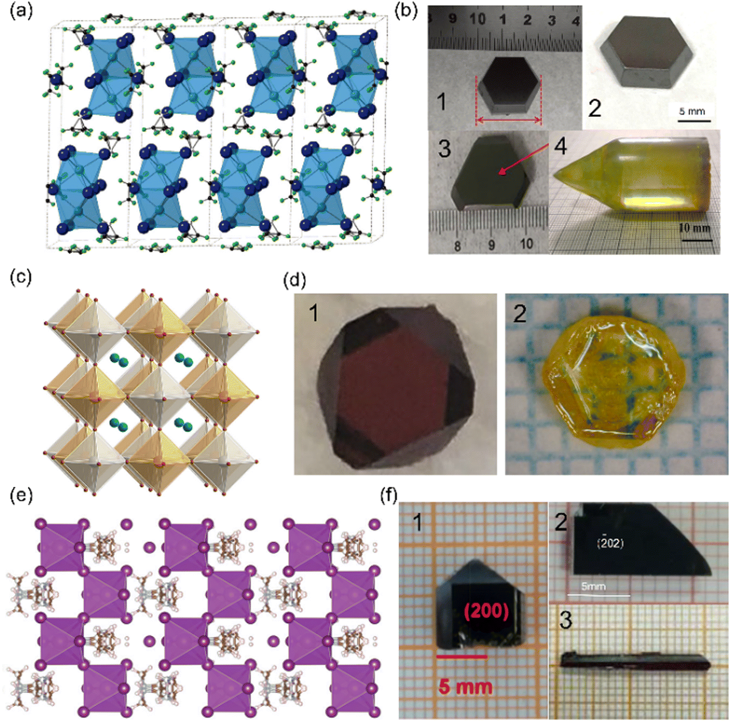 | ||
| Fig. 1 Crystal structures and photographs of bismuth-based perovskite single crystals. (a) Crystal structure of 0D MA3Bi2I9.53 (b) Photographs of A3Bi2X9 single crystals: MA3Bi2I9 (1),53 Cs3Bi2I9 (2),36 and (NH4)3Bi2I9 (3), reproduced with permission,72 Copyright 2019, Springer Nature, Cs3Bi2Br9 (4), reproduced with permission,71 Copyright 2022, American Chemical Society. (c) Crystal structure of 3D Cs2AgBiBr6. Reproduced with permission.86 Copyright 2016, American Chemical Society. (d) Photograph of Cs2AgBiX6 single crystals: Cs2AgBiBr6 (1), reproduced with permission,34 Copyright 2017, Springer Nature, Cs2AgBiCl6 (2), reproduced with permission,74 Copyright 2022, American Chemical Society. (e) Crystal structure of 1D (DMEDA)BiI5.84 (f) Photographs of other-type single crystals: (H2MDAP)BiI5 (1), reproduced with permission,75 Copyright 2019, American Chemical Society, (3-AMP)BiI5 (2), reproduced with permission,76 Copyright 2022, John Wiley & Sons, and (BAH)BiI4 (3), reproduced with permission,77 Copyright 2022, John Wiley & Sons. | ||
For the first time, our research group utilized a seed-crystal-assisted constant-temperature evaporation method to obtain a red hexagonal MA3Bi2I9 crystal with dimensions ∼27 mm × 23 mm × 13 mm.53 The seed crystal was obtained first and was used as the nucleation point to carefully control the nucleation process of the crystal and then kept growing into a large single crystal. Due to its excellent crystal quality, the detector with a vertical Au/MA3Bi2I9/Au configuration exhibited a sensitivity of 10620 μC Gyair−1cm−2. The 0D crystal structure resulted in a high Ea for ion migration (0.46 eV), higher than those reported for 3D MAPbI3 and MAPbBr3 (typically below 0.19 eV), and the bulk resistivity in the out-of-plane direction reached 5.27 × 10¹¹ Ω cm. Consequently, an ultra-low LoD of 0.62 nGyair s−1 was obtained, and the detectors demonstrated stable operation even under high applied biases. Furthermore, no deterioration in detection performance was observed following sensing of an integrated X-ray irradiation dose of ∼23800 mGyair, equivalent to >200000 times the dose required for a single commercial X-ray chest radiograph. Subsequently, Liu's group also developed a different extraneous-nuclei-elimination strategy to grow a large MA3Bi2I9 SC (26 mm in length and 8 mm in height).68 The filtered precursor solution was heated until a large number of tiny crystallites were collected, ensuring that all possible active nucleation sites in the system were consumed. The remaining solution was perfectly saturated to produce a crystal by subsequent cooling growth. By comparing 0D MA3Bi2I9, 2D (PEA)2PbI4, and 3D MAPbI3 under the same conditions, the dark current drift of the MA3Bi2I9 SC detector was seven orders of magnitude lower than that of the 3D MAPbI3 SC, showing huge advantage in ion immigration inhibition of 0D MA3Bi2I9.
We also synthesized the FA3Bi2I9 SC by the nucleation-controlled secondary solution constant temperature evaporation (SSCE) method and the centimeter-sized high-quality crystal showed a full width at half maximum (FWHM) of 0.0096°, indicating the high quality of the single crystal.54 The resistivity of the as-grown FA3Bi2I9 SC was found to be 7.8 × 10¹⁰ Ω cm, and it exhibited a high Ea of 0.56 eV, which was higher than that of MA3Bi2I9, ensuring a low noise level and good operational stability even under large external bias. However, due to the lower μτ product and μ of FA3Bi2I9 compared to MA3Bi2I9, the FA3Bi2I9 SC detector exhibited worse performance with a LoD of 0.2 μGyair s−1 and a sensitivity of 598.1 μC Gyair−1 cm−2. The inorganic Cs3Bi2X9 has also attracted attention due to its stronger X-ray attenuation capability resulting from the heavy Cs element and higher density.36,52,87 However, a large bulk crystal (ϕ 15 × 60 mm3) of Cs3Bi2I9 grown by the vertical Bridgman method exhibited a sensitivity of only 111.9 μC Gyair−1 cm−2, possibly due to the presence of impurities and defects in the crystal. To improve the performance of the detector, Zhang et al. and Wei et al. both fabricated a Cs3Bi2I9 SC using the solvent-grown method, which produced fewer impurities and defects. They developed the refined precursor method and the liquid (silicon oil was used) diffused separation induced crystallization approach, respectively, to control the nucleation of the crystal. As a result, sensitivities of about thousand μC Gyair−1 cm−2 were achieved. However, it is believed that the 0D structure inhibits ionic transport, but also impedes the conduction of carriers at the same time when compared to 3D Pb-based perovskites. For hexagonal structures, the layered structure and high effective masses limit the mobility and diffusion length of charge carriers along the c axis, but utilize better conductivity in the a–b plane for directional charge extraction.88 When the ionic radius of the A site becomes smaller, the 0D A3Bi2X9 type transitions to a 2D-layer structure, which is expected to improve carrier transport and the device performance of bismuth-based perovskites, such as (NH4)3Bi2I9 and Rb3Bi2I9. By optimizing Bridgman vertical growth parameters, defects and voids in the grown 2D Cs3Bi2Br9 crystal can be reduced, resulting in better charge mobility features, thereby improving the X-ray detection performance of the device.71,89Fig. 1(b) shows the photographs of MA3Bi2I9, Cs3Bi2I9, (NH4)3Bi2I9, and Cs3Bi2Br9 SCs.
2.2 Double perovskite Cs2AgBiX6
A Cs2AgBiBr6 double perovskite has been widely investigated recently.34,73,90 The structure of Cs2AgBiX6 is 3D, in which the centers of the metal bromide octahedrons are either occupied by Bi3+ or Ag+, as shown in Fig. 1(c).86 Tang's group reported a 3 × 3 × 2 mm3 Cs2AgBiBr6 SC using an inverse temperature crystallization method.34 Following annealing and surface treatment, the μτ and ρ were found to increase significantly. By further detailed calculations, the effective activation energy for ion migration (considering the contribution from both vacancy formation and vacancy migration) was nearly three times than that of MAPbBr3 SCs. This suggests that ionic migration is indeed more difficult in Cs2AgBiBr6 SCs. Subsequent research has shown that decreasing the temperature from room temperature (RT) to liquid–nitrogen temperature (LN2T) increases the carrier lifetime of Cs2AgBiBr6, resulting in a large increase in detector sensitivity from 316 to 988 μC Gyair−1 cm−2.73 Despite the significant improvement in detector sensitivity, we believe that the application of this method is limited due to the strict requirement for low-temperature technology. In addition, the Cs2AgBiCl6 crystal has been found to exhibit self-powered X-ray detection at zero bias with a sensitivity of 7 μC Gyair−1 cm−2.74 It is hoped that improving the growth process of the single crystals will be beneficial in enhancing the performance of the detectors. Fig. 1(d) shows the photographs of Cs2AgBiBr6 and Cs2AgBiCl6 SCs.2.3 Other types
One-dimensional (1D) materials have also been reported. Generally, the A-site is a larger organic ion, which forms a chain structure by adjusting the ratio of bismuth–iodine octahedron to bismuth–iodine octahedron, with the purpose of enhancing carrier transport performance, as the displayed structure in Fig. 1(e). Fig. 1(f) shows the photographs of some 1D SCs. Reported examples include (H2MDAP)BiI5,75 (DMEDA)BiI5,84 (BAH)BiI477 and (3-AMP)BiI5.76 Among them, except for (BAH)BiI4, which reports excellent device properties, the properties of the remaining materials are not so satisfactory. This also indicates that the increase of dimension does not necessarily improve the detection performance, because their carrier mobility lifetime product is small, unable to effectively collect carriers. In addition, these 1D materials generally grow in small size and are difficult to apply. In the future, further optimization of organic cation size and growth methods to improve carrier mobility, optimize single crystal quality and reduce carrier recombination is the key to further improve detector performance.3 Scalable method
Currently, commonly used imaging methods include point scan imaging (Fig. 2(a)), line scan imaging (Fig. 2(b)), and pixel array imaging, including those with etched electrodes (Fig. 2(c)) and integrated circuits (Fig. 2(d)–(f)). The imaging time for the first two methods is quite long, which is not ideal for reducing radiation damage to the human body. Additionally, the pixel size can affect the resolution of the imaging. For electrode etching, the pixel size cannot be too small due to a lack of a back-end reading circuit. Therefore, the most practical flat-panel medical digital radiographic systems are those based on a large-area integrated circuit. These pixel arrays can be converted into X-ray-sensitive imaging devices by adding a thick active layer, either a scintillator or a photoconductor. Pixel array imaging permits quicker image time and higher spatial resolution. To achieve pixel array imaging, large area perovskite layers on TFT arrays must be fabricated. Considering the difficulty of upscaling single crystals to the required area of at least 100 cm2, a scalable deposition process for polycrystalline perovskite films is necessary. This means that the film should (1) be prepared over a large area, (2) have uniform mass (including uniform thickness and mass), (3) have a thickness thick enough to fully absorb X-rays, (4) be integrated with the TFT panel (which we will discuss in detail later as top-down integration and bottom-up integration), (5) have a carrier mobility lifetime product large enough to reduce carrier recombination, (6) have low dark current to obtain high contrast images, as excessively large dark current may exceed the range of reading circuits, resulting in image contrast reduction, (7) have good stability, including stability of the material itself in the environment, stability under external bias, and stability under irradiation, and reduce ghosting, and (8) have a fast response speed to avoid imaging lag, which affects image quality.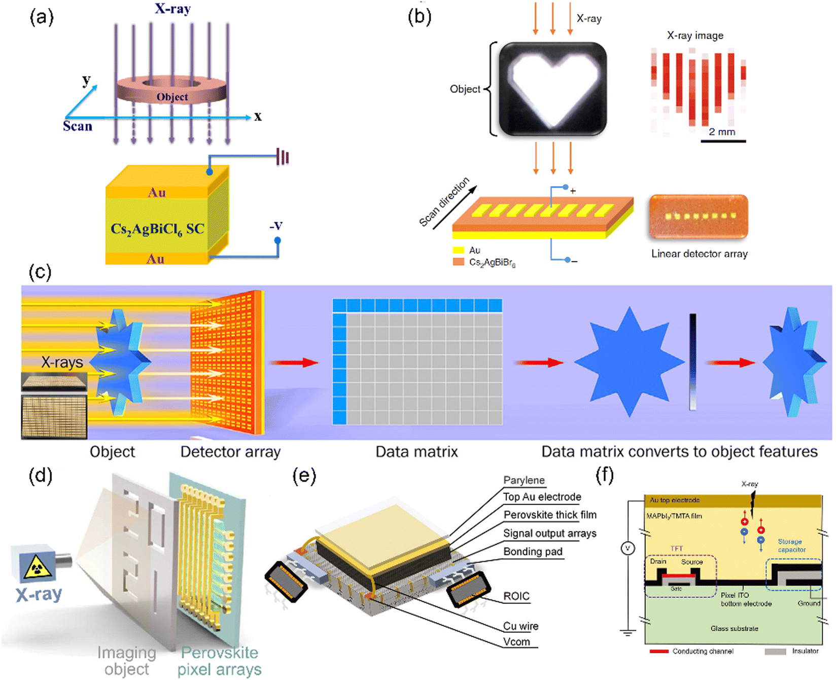 | ||
| Fig. 2 Imaging modes. (a) Point scan imaging. Reproduced with permission.74 Copyright 2022, American Chemical Society. (b) Line scan imaging.83 (c) Pixel array imaging by electrode etching. Reproduced with permission.68 Copyright 2020, Elsevier. (d) Pixel array imaging by integrating with circuit. Reproduced with permission.64 Copyright 2022, Elsevier. (e) Structure of pixel array imaging. (f) Structure of a single pixel. Reproduced with permission.91 Copyright 2022, John Wiley & Sons. | ||
In traditional scintillator detectors, the scintillator is required to be coupled to the detector to function. There are two main coupling methods: substrate pressing (coupling) and direct deposition. In substrate-pressed (coupled) scintillators, the scintillator is grown on a substrate, which is then attached to the detector with the scintillator facing downwards. In direct deposition acicular cesium iodide scintillators, no adhesive or additional substrate is needed, as the scintillator is directly grown on the surface of the flat panel detector (CMOS and TFT plates) using specialized equipment. The same approach applies to direct perovskite detectors. Both bottom-up and top-down methods are available to prepare perovskite layers on the substrate. The bottom-up method involves directly preparing the perovskite layer on the substrate using blade coating, spray coating, evaporation, and other methods, while the top-down method involves first preparing the perovskite layer and then combining it with a binder or by the pressing method. We compare these film-making methods and show the X-ray images obtained by different imaging methods.
3.1 Top-down methods
 | ||
| Fig. 3 Pressing method. (a) MA3Bi2I9 powder to be pressed. Reproduced with permission.78 Copyright 2020, John Wiley & Sons. (b) Schematic diagram of the pressing process.83 (c) Manufactured MAPbI3 wafers. Reproduced with permission.47 Copyright 2020, American Chemical Society. (d) Cross-sectional SEM image of MA3Bi2I9 pellets. (e) IV curve of the MA3Bi2I9 detector. (f) Limit of detection of the MA3Bi2I9 detector. Reproduced with permission.78 Copyright 2020, John Wiley & Sons. (g) Structure of the X-ray imager using the MAPbI3 wafer as the active layer. (h) X-ray images with phantom structure resolution taken by indirect-conversion (left) and the MAPbI3 detector (right). (i) X-ray image of the hearing aid acquired by the MAPbI3 detector.92 | ||
The pressing method has been proved to be a robust and facile process to fabricate thick films. Our group used a cold isostatic pressing process to prepare MA3Bi2I9 pellets with a thickness of millimeters from the MA3Bi2I9 crystal powder.51 The pellets had a tight structure as shown in Fig. 3(d). The resulting pellets had a high resistivity of 2.28 × 10¹¹ Ω cm, making them suitable for low noise devices as shown in Fig. 3(e). The detector made from the pellets achieved a sensitivity of 563 μC Gyair−1 cm−2 and a detection limit of 9.3 nGyair s−1 (Fig. 3(f)), which outperformed commercial a-Se detectors. The detector also exhibited excellent working stability even under high electric fields and large dose irradiation. To simplify the process, the crystal powder was prepared by a low cost antisolvent-assisted synthesis (ASAS) method, in which the precursor solution was dropped into the antisolvent, and a red precipitate was obtained.79 The powder was obtained by washing the red precipitate with chlorobenzene twice and drying in a vacuum oven at 50 °C for 4 h. The Cs alloying resulted in large resistivity and low carrier concentration, which led to an ultralow dark current, making it suitable for detecting radiation at ultralow dose rates. Other Bi-based wafers have also been reported.81 Wei used a Cs3Bi2I9/MXene composite to enhance charge transport.82 Tang's group prepared Cs2AgBiBr6 wafers by using passivated BiOBr, and the resolution is about 4.9 lp mm−1 at MTF = 0.2.83
Shreetu et al. first prepared MAPbI3 wafers whose sensitivity is about 2527 μC Gyair−1 cm−2. But the detectors suffered from serious baseline drift caused by ionic migration.47,94 Subsequently, Sarah et al. successfully integrated a 230 μm-thick MAPbI3 wafer onto an integrated circuit and performed imaging (Fig. 3(g)).92 They established a 10 μm-height photoresist grid on the TFT backplane using photolithography technology. The grid was filled with the MAPbI3 powder, and then the MAPbI3 wafers were liquefied in an atmosphere of methylamine. The recrystallization of the liquefied MAPbI3, due to excessive methylamine evaporation during annealing, was used to bond the wafer to the backplate. The 10 μm photoresist grid served as the mechanical anchoring structure of the thick absorbing layer, enhancing the mechanical adhesion between MAPbI3 and TFT. Finally, the device was capable of resolving 5-line pairs per millimeter (Fig. 3(h)), which is significantly better than indirect detectors. The resolution is around 3 lp mm−1 at MTF = 0.2. Fig. 3(i) shows the X-ray image of the hearing aid acquired by the MAPbI3 detector.
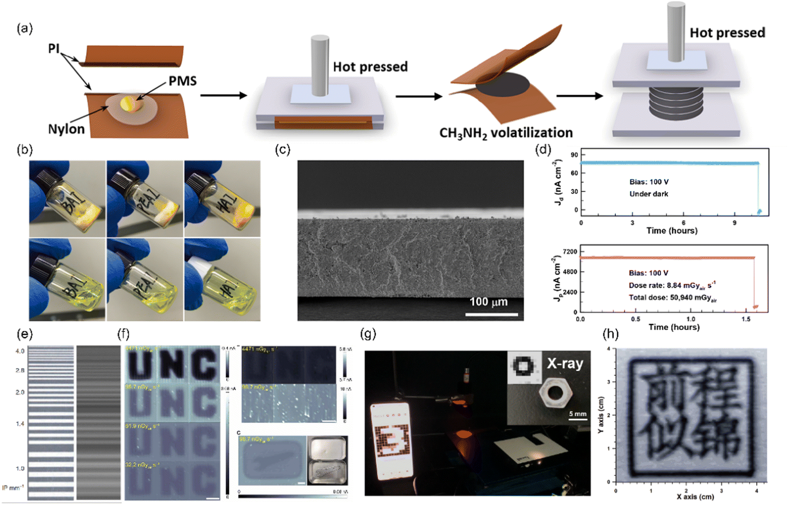 | ||
| Fig. 4 Membrane filling method. (a) Schematic diagram of the membrane filling process. Reproduced with permission.96 Copyright 2021, American Chemical Society. (b) Photograph of the liquid 2D RP perovskite precursors after exposure to CH3NH2 gas. Reproduced with permission.55 Copyright 2022, John Wiley & Sons. (c) Cross sectional SEM image of the MAPbI3 nylon film. Reproduced with permission.96 Copyright 2021, American Chemical Society. (d) Current density in the dark and under radiation of the PentA2MA9Pb10I31 X-ray detector. Reproduced with permission.97 Copyright 2022, American Chemical Society. (e) Photograph (left) and X-ray image (right) of a standard Pb phantom acquired by the MAPb(I0.9Cl0.1)3 detector.98 (f) X-ray imaging of the CsPb0.15FA0.85Pb(Br0.85I0.15)3/Cs0.15FA0.85PbI3 detector.99 (g) Visible-light image and X-ray image of the PentA2MA9Pb10I31 X-ray detector. Reproduced with permission.97 Copyright 2022, American Chemical Society. (h) X-ray imaging of the BA2MA9Pb10I31 X-ray detector. Reproduced with permission.55 Copyright 2022, John Wiley & Sons. | ||
Huang's group successfully prepared a high-concentration MAPbI3 solution using 2-methoxyethanol as the solvent.98 By adding MACl to the precursor, the solution concentration was further increased, resulting in better film filling and reduced gaps caused by solvent evaporation. As a result, the density of the film prepared by them was close to that of the MAPb(I0.9Cl0.1)3 SC, and the loading ratio of the film could reach 95%. They were able to achieve a thickness of about 120 μm for a single film through multiple penetrations from both sides and thermal annealing. By stacking several layers of films together, they obtained a thick film with an area of 400 cm2 and a thickness of several hundred microns. However, due to the large dark current of the 3D lead-based perovskites and the uneven quality of the film, the prepared detector array with 7 × 11 pixels showed poor resolution (Fig. 4(e)), and the spatial resolution was calculated to be 3.5 lp mm−1 when MTF = 0.2. The photocurrent response of each pixel was not uniform, which affected the imaging quality. To address the issue of large dark currents, they applied a heterojunction structure of CsPb0.15FA0.85Pb(Br0.85I0.15)3/CsPb0.15FA0.85PbI3 by laminating the membrane filled with different perovskites.99 The fabricated hetero zjunction device exhibited an obvious rectification of the dark current in the absence of light. Therefore, they chose to use the device at negative bias, which has a much lower dark current density. The signal-to-noise ratio was 800 times that of the pure device, while the sensitivity was not much different, resulting in better imaging quality. Low-dose X-ray images were successfully obtained using their detector, as shown in Fig. 4(f).
Our group has adopted different strategies to inhibit ion migration, reduce dark current, and improve the quality and stability of perovskite films. However, the perovskite precursor typically contains toxic, high-boiling point solvents, such as dimethylformamide (DMF), γ-butyrolactone (GBL), N-methyl-2-pyrrolidone (NMP), and their blends, which are difficult to fully remove from thick films. This can result in lots of holes or cracks in the final perovskite film, which can adversely affect its quality. To address this issue, we synthesized a liquid perovskite molten salt (PMS) of MAPbI3 by exposing a mixture of MAI and PbI2 to CH3NH2 gas (Fig. 4(b)).96 We then infused the PMS into the nylon membrane and fabricated a thick film (LLP, as shown in Fig. 4(c)) by lamination under hot press. We obtained an Ea of 0.54 eV, which is much higher than 0.25 eV obtained for a MAPbI3 SC. This decreased dark current made it possible to observe an obvious X-ray response at a very low dose rate of 14.3 nGyair s−1, indicating good capability of MAPbI3-LLP detectors in detecting X-rays with low dose rates. However, this was still insufficient to achieve high-quality X-ray imaging at low doses. To address this issue, we turned to low-dimensional perovskites, such as quasi-2D Ruddlesden–Popper (RP) perovskites, which have higher ionic activation energy and better intrinsic stability under external stimulations compared to their conventional 3D counterparts. We first reported the solid–liquid transition of 2D RP perovskites enabled by methylamine gas (CH3NH2) and by tuning the quantum well width of RP perovskites through the n value, we successfully provided a hint for solving the trade-off between the stability and detection performance of X-ray detectors.55 A clear X-ray image was obtained using the BA2MA9Pb10I31 (n = 10) detector (Fig. 4(h)). The A-site cation in perovskites decreases the mobility of electrons, leading to low device sensitivity. To balance the ion migration and electron mobility, we chose alkylamines with different carbon chain lengths as the A-site cation to solve the trade-off between the stability and detection performance of X-ray detectors (Fig. 4(d)).97 It was reported that the trimethylolpropane triacrylate (TMTA) additive can be chemically anchored to the grain boundaries of the perovskite to obviously improve its mechanical stability, avoiding the spontaneous detachment of the perovskite film from the substrate. To enhance the bonding force, we added TMTA to the liquified RP perovskite. This resulted in a robust mechanical adhesion between the perovskite and TFT backplane. Fig. 4(g) exhibits a visible-light image and X-ray image acquired using the PentA2MA9Pb10I31 X-ray detector.
Liu's group used a similar method to prepare p-type doped MA3Bi2I9.85 Due to the strong coordination between the dopant 2,3,5,6-tetrafluoro-7,7,8,8-tetracyanoquinodimethane (F4-TCNQ) and MA3Bi2I9, as well as the establishment of a charge-transfer complex, the conductivity improved by four times. The flexible X-ray detector achieved a high sensitivity of 2065 μC Gyair−1 cm−2 with a planar interfingered structure, which can provide a photoconductivity gain. However, this planar structure is not suitable for flat panel imaging, which requires a vertical structure. Therefore, optimizing the structure may further promote its practical application.
3.2 Down-top method
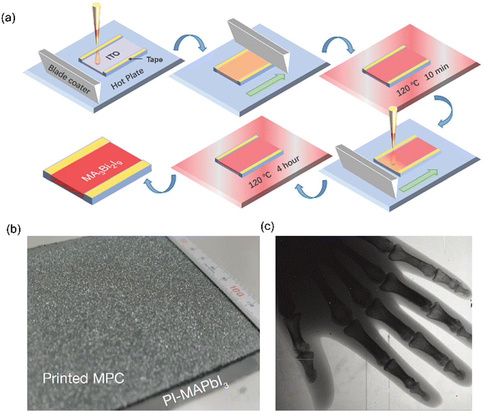 | ||
| Fig. 5 Blade coating method. (a) Schematic diagram of blade coating. (b) Printed MAPbI3 film.80 (c) Hand skeleton image by the MAPbI3 detector. Reproduced with permission.63 Copyright 2017, Springer Nature. | ||
To obtain a thick film, the viscosity of the precursor solution needs to be high enough to leave more precursor material on the substrate. Kim et al. developed a dense and viscous mixture using a two-step solvothermal process.63 First, a high concentration mixture of MAI and PbI2 was prepared with GBL as the solvent, then α-terpineol was added as the anti-solvent to grow MAPbI3 crystals (MPCs). The as-prepared mixture was finally formed into an 830 μm-thick polycrystalline MAPbI3 photoconductor layer using blade coating (Fig. 5(b)). To reduce the dark current of the photoconductor layer, two interlayers of polyimide (PI)-perovskite composites (PI-MAPbBr3 on the top and PI-MAPbI3 on the bottom near TFT backplane) were inserted using spin-casting. The high intrinsic resistivity (1018 Ω cm) of PI was noted to reduce electrical crosstalk among the pixels. The fabricated X-ray detector with an area of 10 × 10 cm2 exhibited a sensitivity of 11000 μC Gyair−1 cm−2, producing a clear image of a hand skeleton (Fig. 5(c)). However, since the crystals are synthesized before solvent evaporation, the obtained thick film has many holes, which leads to a decrease in density, hindering efficient absorption of X-rays. Additionally, these pinholes and defects also impede the collection and transport of carriers. Moreover, not all MPCs adhere well to the substrate, and the size of MPCs (tens of microns) is too large compared to a pixel, which can result in overlapping pixels, leading to charge sharing and substantial degradation of MTF (3.1 lp mm−1 when MTF = 0.2).
Tang's group also fabricated a thick film of MAPbI3 with an area of 28 × 28 cm2 using blade coating.91 They employed soft-pressing to make the blade coating film denser with fewer pinholes. Moreover, they added TMTA to the perovskite precursor to provide a slightly flowing environment and act as a crosslinking agent by in situ polymerization to passivate the defects in the films. The fabricated detector had a low LoD, but the sensitivity was relatively low compared to other MAPbI3 counterparts. The additive TMTA can improve the resistivity, thereby reducing the dark current and improving the ion activation energy to inhibit ion migration. However, the high resistance of TMTA also inhibits the migration and extraction of carriers, which reduces sensitivity.
Ciavatti et al. adopted a cyclic procedure to reduce the size of PbI2, thus allowing them to synthesize MAPbI3 crystals below 1 μm.100 These crystals were then dispersed in propan-2-ol and blade-coated onto a substrate with a planar cross-finger structure. The film's thickness could reach 30 μm by repeating the blade coating process layer by layer. Due to the intrinsic characteristics of the 3D perovskite and the planar cross-finger structure with gain, the sensitivity of the X-ray detector prepared using this film reached 2270 μC Gyair−1 cm−2. However, the detector's dark current was also very large, leading to a high LoD of 27 μGyair s−1, which is unsuitable for low-dose ray detection. Additionally, as mentioned earlier, the planar structure is also unsuitable for pixel array imaging.
Li et al. used green and low-boiling solvents (ethanol and water) instead of traditional toxic and high-boiling solvents.101 They added polyvinyl butyral (PVB) as the binder, and at a concentration of 15% (w/w), it helped in reducing cracks caused by tensile stresses on the top surface during solvent evaporation. In this way, they prepared a 500 μm-thick film with an area of 50 × 75 mm2. They also developed a polymethyl methacrylate (PMMA) film as a blocking layer between the MAPbI3 layer and the aluminum electrode to suppress the dark current. However, the high-resistivity of PVB and PMMA also caused a reduction in the mobility-life product (10−5 cm2 V−1), reducing the sensitivity of detection (22 μC Gyair−1 cm−2) and causing ghosting effects.
Our group achieved the balance between sensitivity and LoD by preparing MA3Bi2I9 using a blade-coating method.80 We used green methylammonium acetate (MAAc) as the solvent and added MACl to improve the film. The twice blade-coated film had a thickness of about 50 μm. Within a certain range, the number of pinholes in the film decreased as the amount of MACl increased, resulting in larger grain size and higher film quality. The 10% MACl-doped MA3Bi2I9 film showed an increased resistivity of 2.7 × 10¹¹ Ω cm and higher mobility compared to other control groups. Furthermore, the 10% MACl-doped MA3Bi2I9 film showed the highest Ea of 0.59 eV, which is much higher than that of the pristine MA3Bi2I9 film (0.46 eV), indicating the suppressed ion migration in the MACl-doped MA3Bi2I9 film. The 10% MACl-doped MA3Bi2I9 detector achieved a sensitivity of 100.16 μC Gyair−1 cm−2 and a LoD of 98.4 nGyair s−1.
Blade coating involves the preparation of a viscous precursor to achieve the desired thickness, but only a small amount of perovskite can be dissolved at extremely high concentrations.
Moreover, some polymers are added to the precursor as binders to reduce dark current and inhibit ion migration to a certain extent, thereby decreasing the detection limit and enhancing the device stability. However, this leads to a significant reduction in the sensitivity of the device. To prevent a large number of holes on the film surface left by solvent evaporation and the solvent in contact with the substrate being sealed and unable to volatilize caused by surface crystallization, low boiling-point solvents or dispersants are recommended. Additionally, the film should be annealed at a low temperature to prevent too rapid surface solvent evaporation.
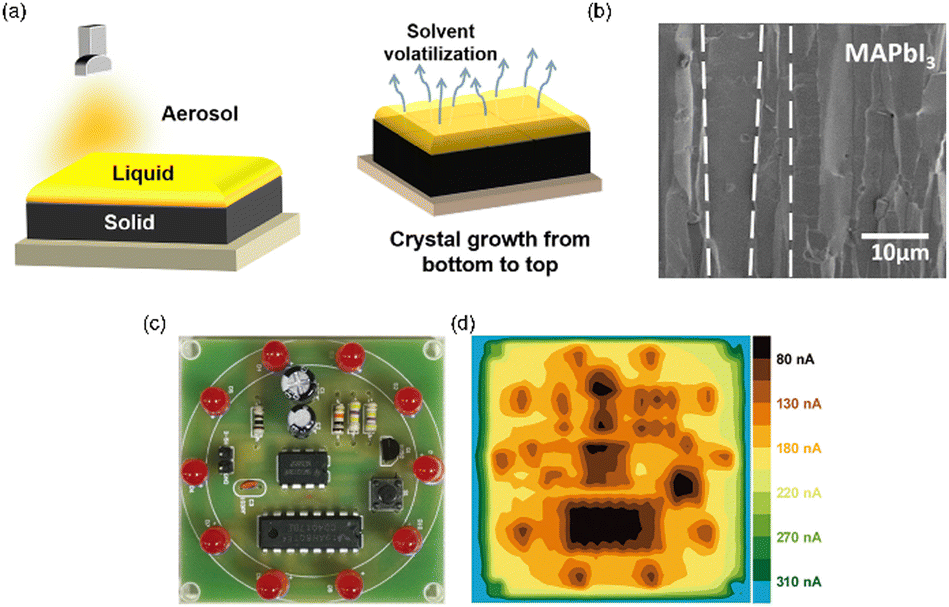 | ||
| Fig. 6 Spray coating method. (a) The schematic diagram of spray coating. (b) Cross sectional SEM image of the MAPbI3 film by spray coating. Reproduced with permission.104 Copyright 2021, Elsevier. (c) Photograph of a circuit. (d) X-ray imaging of the circuit by the 2D (PEA)2MA3Pb4I13/3D MAPbI3 detector.56 | ||
Hirato's group successfully used a mist deposition method to prepare a 20 μm-thick CsPbBr3 film with an area of 25 × 6 mm2. The obtained CsPbBr3 films were composed of highly (101)-oriented columnar crystals when the temperature was 150 °C.102 It was explained that the supply of precursor solution and solvent evaporation were well balanced at 150 °C, resulting in the formation of high-quality films. The columnar crystals were packed closely and had a diameter of 1–2 μm, which was smaller than that of a pixel (typically <100 μm). With the columnar structure, carriers could transport vertically through the whole crystal with few grain boundaries, leading to a high carrier mobility of 13 cm2 V−1 s−1. Crosstalk between pixels may be reduced since lateral traffic was hampered. They then employed a polymer as a buffer layer to prevent the exfoliation of the film when the film became thicker.103 In this way, they prepared a CsPbBr3 film with a thickness of 110 μm and an area of 26 × 10 mm2, which exhibited a sensitivity of 11840 μC Gyair−1 cm−2.
Yang's group utilized an aerosol–liquid–solid process to successfully prepare a CsPbI2Br thick film with an area of 10 × 10 cm2 and a variable thickness ranging from 1 μm to 1 mm.104 This method was found to be applicable for both inorganic and organic–inorganic perovskites, including different dimensional structures such as 3D MAPbI3, 2D (PEA)2PbI4, and 0D Cs3Sb2I9. By maintaining a dynamic equilibrium among the aerosol, liquid, and solid phases, the occurrence of quick nucleation on the surface by solvent evaporation and formation of pinholes due to intrinsic solvent evaporation were avoided, resulting in crystals with large sizes and fewer grain boundaries (Fig. 6(b)). Their device exhibited a high sensitivity of 148000 μC Gyair−1 cm−2 and a low detection limit of 280 nGyair s−1. In addition, they also fabricated a heterojunction structure of 2D (PEA)2MA3Pb4I13/3D MAPbI3 to suppress ion migration in MAPbI3.56 The presence of the 2D perovskite layer increased the detector's resistivity by an order of magnitude, leading to a reduced dark current. Moreover, the detection limit was significantly decreased from 3.10 μGyair s−1 to 480 nGyair s−1. Fig. 6(c) and (d) show the photograph of a circuit and its X-ray image obtained using the 2D (PEA)2MA3Pb4I13/3D MAPbI3 detector.
Our group also developed a thick film of 0D MA3Bi2I9 using the spray coating method.46 We chose green MAAC as the solvent instead of toxic DMF and dimethyl sulphoxide (DMSO). By carefully controlling the crystallization process of the MA3Bi2I9 film with the addition of MACl, we were able to obtain high-quality films with fewer pinholes. The MA3Bi2I9-detector exhibited a resistivity of approximately 5 × 10¹¹ Ω cm and an Ea of 0.91 eV, effectively reducing dark current and ion migration.
The spray coating method can deposit thick perovskite films (with thicknesses of less than 1 mm) over an area of hundreds of square centimeters in a short time through repeated deposition. This method is suitable for most perovskite materials. The crystals in the film obtained by spray coating grow vertically, promoting vertical carrier transport. However, perovskites are inherently toxic, and the use of toxic solvents in the spraying process can result in the dispersion of aerosols in the air, leading to significant air and environmental pollution. Thus, the spraying process is often conducted in a closed glove box.
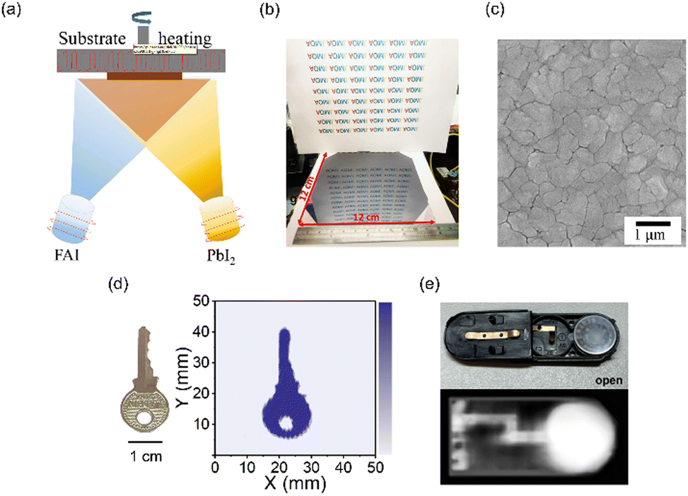 | ||
| Fig. 7 Physical vapor deposition (PVD). (a) Schematic diagram of dual-source evaporation. Reproduced with permissionpermission.105 Copyright 2021, American Chemical Society. (b) Photograph of the CsPbI2Br film. Reproduced with permission.49 Copyright 2022, American Chemical Society. Reproduced with permission.105 Copyright 2021, American Chemical Society. (c) SEM image of the FAPbI3 film. (d) X-ray image of a key using an FAPbI3 detector. (e) X-ray image using a CsPbI2Br detector. Reproduced with permission.49 Copyright 2022, American Chemical Society. | ||
Lin's group developed an in situ substrate heating technique during the dual-source co-evaporation process to prepare a 5 μm-thick FAPbI3 film on a flexible PET substrate (Fig. 7(c)).105 The resulting FAPbI3 detector exhibited a sensitivity of 142.1 μC Gyair−1 cm−2 and showed no severe degradation or deterioration after 4 weeks. Lai reported the preparation of a 1 μm-thick all-inorganic CsPbI2Br film with a p–i–n structure using PVD.49 The film had a surface that was very smooth and mirror-like (Fig. 7(b)), and a LoD of 25.69 nGyair s−1 was achieved. However, the sensitivity of the CsPbI2Br detector was only 1.2 μC Gyair−1 cm−2, likely due to the film thickness not being enough to fully absorb incoming X-rays. The X-ray images obtained by the FAPbI3 and CsPbI2Br detector look blurry (Fig. 7(d) and (e)). Increasing the film thickness may be necessary to improve the detector's sensitivity in future work.
Although PVD is commonly used in scalable filming technology, it is difficult to precisely control the stoichiometry of the dual sources for perovskites. This is because the boiling point of organic salts differs greatly from that of inorganic ones. Additionally, it is time-consuming to prepare a thick film of hundreds of microns using PVD, since the speed of PVD is typically very slow (∼Å s−1 for vacuum evaporation). In the evaporation of a thicker film, the thick film is prone to cracking, and the contact with the substrate is not tight, making it easy to fall off. Therefore, due to the above reasons, the PVD method used to prepare thick films of perovskites has not been extensively studied. Subsequent studies should focus on solving the problems of cracks in the thick film and the contact between the film and substrate. For example, the contact between the film and the substrate may be enhanced by preparing a transition layer on the substrate. Of course, it is inevitable to spend dozens of hours preparing hundreds of microns of thick films, which is relatively time-consuming for scientific research. However, it is worthwhile for large-scale industrial production when the production technology becomes mature.
4 Outlook and summary
To solve the problems faced by 3D lead halide perovskites, many efforts have been made from various aspects. For bismuth-based perovskites, their low-dimensional structure and high ion activation energy make them ideal candidates for low-dose X-ray detection due to their low dark current and excellent stability. However, the blocking effect of a large number of insulating organic cation spacers on carrier transport limits the detection sensitivity. The sensitivity of single and polycrystals may be improved by reducing crystal defects and grain boundaries to reduce carrier recombination. In addition, adjusting the distance and layers of octahedrons by cationic engineering is an effective way to control carrier transport. 2D lead-based perovskites, which combine the stability of low-dimensional perovskites and the excellent photoelectric properties of 3D perovskites, are also an important research direction for X-ray detectors in the future. However, the toxicity of lead should be taken into consideration and any release of Pb into the natural environment should be avoided or at least minimized. Metal-free halide perovskites can be grown from aqueous solution and are eco-friendly, attracting interest in ferroelectrics and X-ray detection.106–109 They have shown long carrier lifetime and large charge diffusion lengths, which benefit charge transport and high sensitivity of X-ray detectors. A flexible and transparent PAZE-NH4X3·H2O detector showed a high spatial resolution of 5 lp mm−1 when MTF = 0.2, which is even better than that of lead-based perovskites. Metal-free halide perovskites will be an important research direction for lead-free high-performance X-ray detectors. Furthermore, ferroelectric assisted X-ray detection has been proved to be an effective strategy to decrease dark current introduced by large external bias. Moreover, ferroelectrics can provide an intrinsic driving force to separate electron–hole pairs generated by X-rays without severe ionic migration problems.57,59–62Most reported halide perovskite X-ray detectors have a simple metal–perovskite–metal structure and advanced device structure design can further boost the detection performance of X-ray detectors. Template (porous anodic aluminum oxide) growth of CsPbBr2I is shown to be a useful method to reduce the dark current, ionic migration and pixel–pitch crosstalk.50 Polyimide–perovskite composites were used as interlayers to reduce the dark current.63 Through cautiously optimizing the device structure including the structures of perovskites and interlayers, more stable and sensitive X-ray detectors can be acquired. Besides, using avalanche diodes may amplify the photoelectric signals and improve the detection sensitivity. To achieve high quality X-ray imaging, large, thick and uniform films are needed. Top-down methods such as the pressing method and membrane filling method can ensure adequate thickness of the active layer. It is important to note that for the pressing method, the fluidity of the powder and the used pressure can introduce non-uniformity of the perovskite film. Due to brittleness and low decomposition temperature, perovskites cannot be granulated with traditional binders (such as polyvinyl alcohol (PVA)) to improve fluidity, resulting in the cracking of large-size films. Research on binders for low temperature (below 300 °C) to improve the fluidity of the powder is the main direction of development. For the membrane filling method, the non-uniform loading of perovskites on nylon membranes will lead to poor imaging of the detector. Consequent treatment of membranes, such as isostatic pressing, is conducive to obtaining uniform thick membranes.
For multi-pixel detectors, not only the optoelectronic properties of the active layer should be considered, but also the integration with the circuit. For top-down methods, although liquefied perovskites have been used as binders, their bonding effect is not satisfactory, affecting the carrier transport and device performance. Adhesives for bonding the perovskite film with the substrate need to be developed to ensure that the photoelectric properties of the film are not compromised during the bonding process. For bottom-up methods, simplicity, applicability, environmental protection, and reliability of the method should be considered comprehensively. However, applying similar technology to obtain the micron or millimeter-level thick films requires exploring new process conditions. This is because the film's crystallization growth process becomes more complex as the thickness increases, the extrusion of grain growth leads to the thick film being prone to cracking, and it is difficult to remove the solvent completely in thick perovskite films, thus affecting the density of the film and the bonding features with the substrate. Solvent-free methods, such as methylamine liquefaction of lead-based perovskites, can avoid the effects of solvents, but this method is unsuitable for FA- or Cs-based perovskites. In the growth process of perovskite films, polymer additives can increase the viscosity of the precursor, regulate crystal growth, release stress, and bond the substrate. However, the addition of polymers can also seriously affect the performance of perovskite X-ray detectors, and the development of polymers with semiconductor properties as additives may alleviate this problem.
Metrics for the performance of perovskite detectors should be standardized to enable comparisons between different detectors and obtain valuable information to advance the development of the field. Sensitivity (S) is a commonly used parameter defined as the density of charge produced per unit radiation dose. In practice, sensitivity is the quotient of signal current density and dose rate. The higher the sensitivity, the better the detector responds to X-rays. However, this is not absolute, as the sensitivity is also closely related to the tube voltage of the incident X-ray. That is, at the same X-ray dose rate, using a higher tube voltage always yields a higher calculated sensitivity than using a lower tube voltage. Therefore, sensitivities obtained at different tube voltages are not comparable. It is necessary to evaluate the performance of the detector under specified standard conditions. We therefore recommend the use of normalized sensitivity. Theoretical sensitivity (S0) refers to the sensitivity under ideal conditions where all incident rays are absorbed and all generated charge carriers are collected. Theoretical sensitivity is a constant, dependent only on the energy of the incident ray and the band gap of the active layer itself. The normalized sensitivity (S/S0) is defined as the ratio of measured sensitivity and theoretical sensitivity. This value represents the actual detection efficiency of different detectors and reflects the detection performance of detectors at a certain energy.
The dynamic range is a critical performance metric for X-ray detectors as it reflects the range of radiation energy levels that the device can detect. The maximum detected radiation energy corresponds to the energy at which the detector reaches the saturation current, while the minimum detected radiation energy is often related to the level of dark current and noise in the system. The linear dynamic range, which is defined as the range of signal current and radiation energy exhibiting a linear relationship, is an important parameter that determines the dose range over which the detector can maintain a constant sensitivity. It is crucial for the linear dynamic range to be wide enough to ensure that the detector can acquire accurate information about the detected object, while avoiding saturation or noise. Therefore, we suggest that future studies pay more attention to the linear dynamic range of the detected materials.
Spatial resolution is used to measure a detector's ability to distinguish two objects that are very close. Spatial resolution is usually expressed by calculating the value of modulation transfer function (MTF), which can be used to compare the performance of different detectors. But in the published literature, only a few articles focused on this metric and most articles lack research on spatial resolution.63,83,92,93,95,98 Though the halide perovskites have reached a high sensitivity, the spatial resolution is unremarkable and mostly lies in the range of 3–5 lp mm−1 when MTF = 0.2. The spatial resolution is influenced by the pixel size of the detector, the collimator gap, the shape and size of the beam. Further adjustment of these factors can help in improving the spatial resolution of detectors.
Conflicts of interest
There are no conflicts to declare.Acknowledgements
This work was supported by the National Natural Science Foundation of China (grant no. NSFC62004182, NSFC52032007, and NSFC51932010), the Sichuan Science and Technology Program (grant no. 2022JDRC0021, 2021JDTD0021), and the Career Development Grant of Institute of Chemical Materials (STB-2021-10).Notes and references
- V. V. Nagarkar, T. K. Gupta, S. R. Miller and Y. Klugerman, IEEE Trans. Nucl. Sci., 1998, 45, 492–496 CAS.
- W. Heiss and C. Brabec, Nat. Photonics, 2016, 10, 288–289 CrossRef CAS.
- V. F. Dvoryankin, G. G. Dvoryankina, A. A. Kudryashov, A. G. Petrov, V. D. Golyshev and S. V. Bykova, Tech. Phys., 2010, 55, 306–308 CrossRef CAS.
- M. Schiebera, H. Hermon, A. Zuck, A. Vilensky, L. Melekhov, R. Shatunovsky, E. Meerson, Y. Saado, M. Lukach, E. Pinkhasy, S. E. Ready and R. A. Street, J. Cryst. Growth, 2001, 225, 118–123 CrossRef.
- K. S. Shah, R. A. Street, Y. Dmitriyev, P. Bennett, L. Cirignano, M. Klugerman and M. R. Squillante, Nucl. Instrum. Methods Phys. Res., Sect. A, 2001, 458, 140–147 CrossRef CAS.
- D. M. Hunter, G. Belev, S. Kasap and M. J. Yaffe, Med. Phys., 2012, 39, 608–622 CrossRef CAS PubMed.
- S. D. Sordo, L. Abbene, E. Caroli, A. M. Mancini, A. Zappettini and P. Ubertini, Sensors, 2009, 9, 3491–3526 CrossRef PubMed.
- W. R. Hendee and M. K. O’Connor, Radiology, 2012, 264, 312–321 CrossRef PubMed.
- E. K. Kerut and F. To, Echocardiography, 2011, 28, 593–595 CrossRef PubMed.
- E. C. Lin, Mayo Clin. Proc., 2010, 85, 1142–1146 CrossRef PubMed.
- D. A. Schauer and O. W. Linton, Radiology, 2009, 253, 293–296 CrossRef PubMed.
- D. Y. Xin, S. J. Tie, R. H. Yuan, X. J. Zheng, J. G. Zhu and W. H. Zhang, ACS Appl. Mater. Interfaces, 2019, 11, 44233–44240 CrossRef CAS PubMed.
- D. Y. Xin, S. J. Tie, X. J. Zheng, J. G. Zhu and W. H. Zhang, J. Energy Chem., 2020, 46, 173–177 CrossRef.
- N. Zhou and H. Zhou, Small Struct., 2022, 3, 2100232 CrossRef CAS.
- A. Younis, C. H. Lin, X. Guan, S. Shahrokhi, C. Y. Huang, Y. Wang, T. He, S. Singh, L. Hu, J. R. D. Retamal, J. H. He and T. Wu, Adv. Mater., 2021, 33, 2005000 CrossRef CAS PubMed.
- Y. Dong, Y. Zou, J. Song, X. Song and H. Zeng, J. Mater. Chem. C, 2017, 5, 11369–11394 RSC.
- Y. Wu, J. Feng, Z. Yang, Y. Liu and S. F. Liu, Adv. Sci., 2022, 10, 2205536 CrossRef PubMed.
- Y. Wang, H. Lou, C.-Y. Yue and X.-W. Lei, CrystEngComm, 2022, 24, 2201–2212 RSC.
- H. Hu, G. Niu, Z. Zheng, L. Xu, L. Liu and J. Tang, EcoMat, 2022, 4, e12258 CAS.
- R. Chaudhari and C. RaviKant, Sens. Actuators, A, 2022, 346, 113863 CrossRef CAS.
- J. Ghosh, P. J. Sellin and P. K. Giri, Nanotechnology, 2022, 33, 312001 CrossRef PubMed.
- J. Li, J. Duan, X. Yang, Y. Duan, P. Yang and Q. Tang, Nano Energy, 2021, 80, 105526 CrossRef CAS.
- N. Leupold and F. Panzer, Adv. Funct. Mater., 2021, 31, 2007350 CrossRef CAS.
- X. Xu, W. Qian, S. Xiao, J. Wang, S. Zheng and S. Yang, EcoMat, 2020, 2, e12064 CAS.
- L. Lu, X. Pan, J. Luo and Z. Sun, Chem. – Eur. J., 2020, 26, 16975–16984 CrossRef CAS PubMed.
- G. Kakavelakis, M. Gedda, A. Panagiotopoulos, E. Kymakis, T. D. Anthopoulos and K. Petridis, Adv. Sci., 2020, 2002098 CrossRef CAS PubMed.
- C. Wu, Q. Zhang, G. Liu, Z. Zhang, D. Wang, B. Qu, Z. Chen and L. Xiao, Adv. Energy Mater., 2019, 10, 1902496 CrossRef.
- J. Shamsi, A. S. Urban, M. Imran, L. De Trizio and L. Manna, Chem. Rev., 2019, 119, 3296–3348 CrossRef CAS PubMed.
- P. Wangyang, C. Gong, G. Rao, K. Hu, X. Wang, C. Yan, L. Dai, C. Wu and J. Xiong, Adv. Opt. Mater., 2018, 6, 1701302 CrossRef.
- Q. Chen, J. Wu, X. Ou, B. Huang, J. Almutlaq, A. A. Zhumekenov, X. Guan, S. Han, L. Liang, Z. Yi, J. Li, X. Xie, Y. Wang, Y. Li, D. Fan, D. B. L. Teh, A. H. All, O. F. Mohammed, O. M. Bakr, T. Wu, M. Bettinelli, H. Yang, W. Huang and X. Liu, Nature, 2018, 561, 88–93 CrossRef CAS PubMed.
- R. Babu, L. Giribabu and S. P. Singh, Cryst. Growth Des., 2018, 18, 2645–2664 CrossRef CAS.
- H. Wei, Y. Fang, P. Mulligan, W. Chuirazzi, H.-H. Fang, C. Wang, B. R. Ecker, Y. Gao, M. A. Loi, L. Cao and J. Huang, Nat. Photonics, 2016, 10, 333–339 CrossRef CAS.
- H. Wei, D. DeSantis, W. Wei, Y. Deng, D. Guo, T. J. Savenije, L. Cao and J. Huang, Nat. Mater., 2017, 16, 826–833 CrossRef CAS PubMed.
- W. Pan, H. Wu, J. Luo, Z. Deng, C. Ge, C. Chen, X. Jiang, W.-J. Yin, G. Niu, L. Zhu, L. Yin, Y. Zhou, Q. Xie, X. Ke, M. Sui and J. Tang, Nat. Photonics, 2017, 11, 726–732 CrossRef CAS.
- Y. Liu, Y. Zhang, X. Zhu, J. Feng, I. Spanopoulos, W. Ke, Y. He, X. Ren, Z. Yang, F. Xiao, K. Zhao, M. Kanatzidis and S. F. Liu, Adv. Mater., 2021, 33, e2006010 CrossRef PubMed.
- Y. Zhang, Y. Liu, Z. Xu, H. Ye, Z. Yang, J. You, M. Liu, Y. He, M. G. Kanatzidis and S. F. Liu, Nat. Commun., 2020, 11, 2304 CrossRef CAS PubMed.
- Y. Liu, Y. Zhang, K. Zhao, Z. Yang, J. Feng, X. Zhang, K. Wang, L. Meng, H. Ye, M. Liu and S. F. Liu, Adv. Mater., 2018, 30, 1707314 CrossRef PubMed.
- Y. Liu, Y. Zhang, Z. Yang, H. Ye, J. Feng, Z. Xu, X. Zhang, R. Munir, J. Liu, P. Zuo, Q. Li, M. Hu, L. Meng, K. Wang, D. M. Smilgies, G. Zhao, H. Xu, Z. Yang, A. Amassian, J. Li, K. Zhao and S. F. Liu, Nat. Commun., 2018, 9, 5302 CrossRef CAS PubMed.
- Y. Liu, X. Ren, J. Zhang, Z. Yang, D. Yang, F. Yu, J. Sun, C. Zhao, Z. Yao, B. Wang, Q. Wei, F. Xiao, H. Fan, H. Deng, L. Deng and S. F. Liu, Sci. China: Chem., 2017, 60, 1367–1376 CrossRef CAS.
- Y. Zhang, Y. Liu, Y. Li, Z. Yang and S. Liu, J. Mater. Chem. C, 2016, 4, 9172–9178 RSC.
- Y. Liu, Y. Zhang, Z. Yang, D. Yang, X. Ren, L. Pang and S. F. Liu, Adv. Mater., 2016, 28, 9204–9209 CrossRef CAS PubMed.
- Y. Liu, J. Sun, Z. Yang, D. Yang, X. Ren, H. Xu, Z. Yang and S. F. Liu, Adv. Opt. Mater., 2016, 4, 1829–1837 CrossRef CAS.
- Y. Liu, Z. Yang, D. Cui, X. Ren, J. Sun, X. Liu, J. Zhang, Q. Wei, H. Fan, F. Yu, X. Zhang, C. Zhao and S. F. Liu, Adv. Mater., 2015, 27, 5176–5183 CrossRef CAS PubMed.
- H. Li, X. Shan, J. N. Neu, T. Geske, M. Davis, P. Mao, K. Xiao, T. Siegrist and Z. Yu, J. Mater. Chem. C, 2018, 6, 11961–11967 RSC.
- H. Zhang, G. Dun, Q. Feng, R. Zhao, R. Liang, Z. Gao, T. Hirtz, M. Chen, X. Geng, M. Liu, Y. Huang, X. Zheng, K. Qin, X. Tan, X. Wang, D. Xie, Y. Yang, H. Tian, Y. Zhou, N. P. Padture, X. Wang, J. Hong and T.-L. Ren, IEEE Trans. Electron Devices, 2020, 67, 3191–3198 CAS.
- D. Xin, S. Dong, M. Zhang, S. Tie, J. Ren, L. Lei, P. Yu, J. Zhu, Y. Zhao and X. Zheng, J. Phys. Chem. Lett., 2022, 13, 371–377 CrossRef CAS PubMed.
- M. Hu, S. Jia, Y. Liu, J. Cui, Y. Zhang, H. Su, S. Cao, L. Mo, D. Chu, G. Zhao, K. Zhao, Z. Yang and S. F. Liu, ACS Appl. Mater. Interfaces, 2020, 12, 16592–16600 CrossRef CAS PubMed.
- S. Yakunin, M. Sytnyk, D. Kriegner, S. Shrestha, M. Richter, G. J. Matt, H. Azimi, C. J. Brabec, J. Stangl, M. V. Kovalenko and W. Heiss, Nat. Photonics, 2015, 9, 444–449 CrossRef CAS PubMed.
- P. T. Lai, H. C. Lin, Y. T. Chuang, C. Y. Chen, W. K. Cheng, G. H. Tan, B. W. Hsu, L. Yang, S. C. Lou, L. J. Chien, H. W. Wang and H. W. Lin, ACS Appl. Mater. Interfaces, 2022, 14, 19795–19805 CrossRef CAS PubMed.
- M. Zhu, X. Du, G. Niu, W. Liu, W. Pan, J. Pang, W. Wang, C. Chen, Y. Xu and J. Tang, Fundam. Res., 2022, 2, 108–113 CrossRef CAS.
- S. Tie, W. Zhao, D. Xin, M. Zhang, J. Long, Q. Chen, X. Zheng, J. Zhu and W. H. Zhang, Adv. Mater., 2020, 32, 2001981 CrossRef CAS PubMed.
- S. Wei, S. Tie, K. Shen, T. Zeng, J. Zou, Y. Huang, H. Sun, L. Luo, X. Zhou, A. Ren, X. Zheng, D. Zhao and J. Wu, Adv. Opt. Mater., 2021, 9, 2101351 CrossRef CAS.
- X. Zheng, W. Zhao, P. Wang, H. Tan, M. I. Saidaminov, S. Tie, L. Chen, Y. Peng, J. Long and W.-H. Zhang, J. Energy Chem., 2020, 49, 299–306 CrossRef.
- W. Li, D. Xin, S. Tie, J. Ren, S. Dong, L. Lei, X. Zheng, Y. Zhao and W. H. Zhang, J. Phys. Chem. Lett., 2021, 12, 1778–1785 CrossRef CAS PubMed.
- M. Zhang, D. Xin, S. Dong, W. Zhao, S. Tie, B. Cai, Q. Ma, Q. Chen, W. H. Zhang and X. Zheng, Adv. Opt. Mater., 2022, 10, 2201548 CrossRef CAS.
- X. Xu, W. Qian, J. Wang, J. Yang, J. Chen, S. Xiao, Y. Ge and S. Yang, Adv. Sci., 2021, 8, e2102730 CrossRef PubMed.
- C. Ji, S. Wang, Y. Wang, H. Chen, L. Li, Z. Sun, Y. Sui, S. Wang and J. Luo, Adv. Funct. Mater., 2019, 30, 1905529 CrossRef.
- X. Liu, S. Wang, P. Long, L. Li, Y. Peng, Z. Xu, S. Han, Z. Sun, M. Hong and J. Luo, Angew. Chem., Int. Ed., 2019, 58, 14504–14508 CrossRef CAS PubMed.
- W. Guo, X. Liu, S. Han, Y. Liu, Z. Xu, M. Hong, J. Luo and Z. Sun, Angew. Chem., Int. Ed., 2020, 59, 13879–13884 CrossRef CAS PubMed.
- C. Ji, Y. Li, X. Liu, Y. Wang, T. Zhu, Q. Chen, L. Li, S. Wang and J. Luo, Angew. Chem., Int. Ed., 2021, 60, 20970–20976 CrossRef CAS PubMed.
- C. F. Wang, H. Li, M. G. Li, Y. Cui, X. Song, Q. W. Wang, J. Y. Jiang, M. M. Hua, Q. Xu, K. Zhao, H. Y. Ye and Y. Zhang, Adv. Funct. Mater., 2021, 31, 2009457 CrossRef CAS.
- C. F. Wang, H. Li, Q. Ji, C. Ma, L. Liu, H. Y. Ye, B. Cao, G. Yuan, H. F. Lu, D. W. Fu, M. G. Ju, J. Wang, K. Zhao and Y. Zhang, Adv. Funct. Mater., 2022, 32, 2205918 CrossRef CAS.
- Y. C. Kim, K. H. Kim, D. Y. Son, D. N. Jeong, J. Y. Seo, Y. S. Choi, I. T. Han, S. Y. Lee and N. G. Park, Nature, 2017, 550, 87–91 CrossRef CAS PubMed.
- J. Peng, Y. Xu, F. Yao, H. Huang, R. Li and Q. Lin, Matter, 2022, 5, 2251–2264 CrossRef CAS.
- J. Li, H. L. Cao, W. B. Jiao, Q. Wang, M. Wei, I. Cantone, J. Lu and A. Abate, Nat. Commun., 2020, 11, 310 CrossRef CAS PubMed.
- M. Lyu, J.-H. Yun, M. Cai, Y. Jiao, P. V. Bernhardt, M. Zhang, Q. Wang, A. Du, H. Wang, G. Liu and L. Wang, Nano Res., 2016, 9, 692–702 CrossRef CAS.
- M. Abulikemu, S. Ould-Chikh, X. Miao, E. Alarousu, B. Murali, G. O. N. Ndjawa, J. Barbe, A. E. Labban, A. Amassiana and S. D. Gobbo, J. Mater. Chem. A, 2016, 4, 12504–12515 RSC.
- Y. Liu, Z. Xu, Z. Yang, Y. Zhang, J. Cui, Y. He, H. Ye, K. Zhao, H. Sun, R. Lu, M. Liu, M. G. Kanatzidis and S. Liu, Matter, 2020, 3, 180–196 CrossRef.
- Q. Sun, Y. Xu, H. Zhang, B. Xiao, X. Liu, J. Dong, Y. Cheng, B. Zhang, W. Jie and M. G. Kanatzidis, J. Mater. Chem. A, 2018, 6, 23388–23395 RSC.
- M. Xia, J. H. Yuan, G. Niu, X. Du, L. Yin, W. Pan, J. Luo, Z. Li, H. Zhao, K. H. Xue, X. Miao and J. Tang, Adv. Funct. Mater., 2020, 30, 1910648 CrossRef CAS.
- X. Li, P. Zhang, Y. Hua, F. Cui, X. Sun, L. Liu, Y. Bi, Z. Yue, G. Zhang and X. Tao, ACS Appl. Mater. Interfaces, 2022, 14, 9340–9351 CrossRef CAS PubMed.
- R. Zhuang, X. Wang, W. Ma, Y. Wu, X. Chen, L. Tang, H. Zhu, J. Liu, L. Wu, W. Zhou, X. Liu and Y. Yang, Nat. Photonics, 2019, 13, 602 CrossRef CAS.
- J. A. Steele, W. Pan, C. Martin, M. Keshavarz, E. Debroye, H. Yuan, S. Banerjee, E. Fron, D. Jonckheere, C. W. Kim, W. Baekelant, G. Niu, J. Tang, J. Vanacken, M. Van der Auweraer, J. Hofkens and M. B. J. Roeffaers, Adv. Mater., 2018, 30, e1804450 CrossRef PubMed.
- N. K. Tailor, J. Ghosh, M. A. Afroz, S. Bennett, M. Chatterjee, P. Sellin and S. Satapathi, ACS Appl. Electron. Mater., 2022, 4, 4530–4539 CrossRef CAS.
- K. Tao, Y. Li, C. Ji, X. Liu, Z. Wu, S. Han, Z. Sun and J. Luo, Chem. Mater., 2019, 31, 5927–5932 CrossRef CAS.
- X. Yang, Y. H. Huang, X. D. Wang, W. G. Li and D. B. Kuang, Angew. Chem., Int. Ed., 2022, 81, e202204663 Search PubMed.
- C. Ma, H. Li, M. Chen, Y. Liu, K. Zhao and S. Liu, Adv. Funct. Mater., 2022, 32, 2202160 CrossRef CAS.
- S. Tie, W. Zhao, D. Xin, M. Zhang, J. Long, Q. Chen, X. Zheng, J. Zhu and W. H. Zhang, Adv. Mater., 2020, e2001981 CrossRef PubMed.
- S. Tie, D. Xin, S. Dong, B. Cai, J. Zhu and X. Zheng, ACS Sustainable Chem. Eng., 2022, 10, 10743–10751 CrossRef CAS.
- S. Dong, D. Xin, M. Zhang, S. Tie, B. Cai, Q. Ma and X. Zheng, J. Mater. Chem. C, 2022, 10, 6236–6242 RSC.
- N. Bu, S. Jia, Y. Xiao, H. Li, N. Li, X. Liu, Z. Yang, K. Zhao and S. Liu, J. Mater. Chem. C, 2022, 22, 6665–6672 RSC.
- S. Wei, S. Tie, K. Shen, H. Sun, X. Zheng, H. Wang, W. Liang, J. Zou, Y. Huang, L. Luo, X. Zhou, T. Zeng, A. Ren, D. Zhao and J. Wu, Adv. Opt. Mater., 2022, 10, 2201585 CrossRef CAS.
- B. Yang, W. Pan, H. Wu, G. Niu, J. H. Yuan, K. H. Xue, L. Yin, X. Du, X. S. Miao, X. Yang, Q. Xie and J. Tang, Nat. Commun., 2019, 10, 1989 CrossRef PubMed.
- L. Yao, G. Niu, L. Yin, X. Du, Y. Lin, X. Den, J. Zhang and J. Tang, J. Mater. Chem. C, 2020, 8, 1239–1243 RSC.
- X. Liu, H. Li, Q. Cui, S. Wang, C. Ma, N. Li, N. Bu, T. Yang, X. Song, Y. Liu, Z. Yang, K. Zhao and S. F. Liu, Angew. Chem., Int. Ed., 2022, 61, e202209320 CAS.
- A. H. Slavney, T. Hu, A. M. Lindenberg and H. I. Karunadasa, J. Am. Chem. Soc., 2016, 138, 2138–2141 CrossRef CAS PubMed.
- H. Zhang, Y. Xu, Q. Sun, J. Dong, Y. Lu, B. Zhang and W. Jie, CrystEngComm, 2018, 20, 4935–4941 RSC.
- M. Pazoki, M. B. Johansson, H. Zhu, P. Broqvist, T. Edvinsson, G. Boschloo and E. M. J. Johansson, J. Phys. Chem. C, 2016, 120, 29039–29046 CrossRef CAS.
- X. Li, X. Du, P. Zhang, Y. Hua, L. Liu, G. Niu, G. Zhang, J. Tang and X. Tao, Sci. China Mater., 2021, 64, 1427–1436 CrossRef CAS.
- V. Murgulov, C. Schweinle, M. Daub, H. Hillebrecht, M. Fiederle, V. Dědič and J. Franc, J. Mater. Sci., 2022, 57, 2758–2774 CrossRef CAS.
- M. Xia, Z. Song, H. Wu, X. Du, X. He, J. Pang, H. Luo, L. Jin, G. Li, G. Niu and J. Tang, Adv. Funct. Mater., 2022, 2110729 CrossRef CAS.
- S. Deumel, A. van Breemen, G. Gelinck, B. Peeters, J. Maas, R. Verbeek, S. Shanmugam, H. Akkerman, E. Meulenkamp, J. E. Huerdler, M. Acharya, M. García-Batlle, O. Almora, A. Guerrero, G. Garcia-Belmonte, W. Heiss, O. Schmidt and S. F. Tedde, Nat. Electron, 2021, 4, 681–688 CrossRef CAS.
- L. Liu, W. Li, X. Feng, C. Guo, H. Zhang, H. Wei and B. Yang, Adv. Sci., 2022, e2103735 CrossRef PubMed.
- S. Shrestha, R. Fischer, G. J. Matt, P. Feldner, T. Michel, A. Osvet, I. Levchuk, B. Merle, S. Golkar, H. Chen, S. F. Tedde, O. Schmidt, R. Hock, M. Rührig, M. Göken, W. Heiss, G. Anton and C. J. Brabec, Nat. Photonics, 2017, 11, 436–440 CrossRef CAS.
- H. Chen, B. An, G. Peng, S. Wang, Z. Li, J. Sun, W. Lan, J. Fu, H. Wang, L. Ding and Z. Jin, Adv. Opt. Mater., 2022, 2202157 Search PubMed.
- M. Zhang, W. Zhao, D. Xin, L. Lei, J. Long, Y. Zhao, J. Zhu, X. Zheng, Q. Chen and W. H. Zhang, J. Phys. Chem. Lett., 2021, 12, 6961–6966 CrossRef CAS PubMed.
- D. Xin, M. Zhang, Z. Fan, N. Yang, R. Yuan, B. Cai, P. Yu, J. Zhu and X. Zheng, J. Phys. Chem. Lett., 2022, 11928–11935 CrossRef CAS PubMed.
- J. Zhao, L. Zhao, Y. Deng, X. Xiao, Z. Ni, S. Xu and J. Huang, Nat. Photonics, 2020, 14, 612 CrossRef.
- Y. Zhou, L. Zhao, Z. Ni, S. Xu, J. Zhao, X. Xiao and J. Huang, Sci. Adv., 2021, 7, 6716 CrossRef PubMed.
- A. Ciavatti, R. Sorrentino, L. Basiricò, B. Passarella, M. Caironi, A. Petrozza and B. Fraboni, Adv. Funct. Mater., 2020, 2009072 Search PubMed.
- Y. Li, E. Adeagbo, C. Koughia, B. Simonson, R. D. Pettipas, A. Mishchenko, S. M. Arnab, L. Laperrière, G. Belev, A. L. Stevens, S. O. Kasap and T. L. Kelly, J. Mater. Chem. C, 2022, 10, 1228–1235 RSC.
- Y. Haruta, T. Ikenoue, M. Miyake and T. Hirato, Appl. Phys. Express, 2019, 12, 085505 CrossRef CAS.
- Y. Haruta, T. Ikenoue, M. Miyake and T. Hirato, MRS Adv., 2020, 5, 395–401 CrossRef CAS.
- W. Qian, X. Xu, J. Wang, Y. Xu, J. Chen, Y. Ge, J. Chen, S. Xiao and S. Yang, Matter, 2021, 4, 942–954 CrossRef CAS.
- W. Li, Y. Xu, J. Peng, R. Li, J. Song, H. Huang, L. Cui and Q. Lin, ACS Appl. Mater. Interfaces, 2021, 13, 2971–2978 CrossRef CAS PubMed.
- H. Ye, Y. Tang, P. Li, W. Liao, J. Gao, X. Hua, H. Cai, P. Shi, Y. You and R. Xiong, Science, 2018, 361, 151–155 CrossRef CAS PubMed.
- X. Song, Q. Li, J. Han, C. Ma, Z. Xu, H. Li, P. Wang, Z. Yang, Q. Cui, L. Gao, Z. Quan, S. F. Liu and K. Zhao, Adv. Mater., 2021, 33, e2102190 CrossRef PubMed.
- X. Song, Q. Cui, Y. Liu, Z. Xu, H. Cohen, C. Ma, Y. Fan, Y. Zhang, H. Ye, Z. Peng, R. Li, Y. Chen, J. Wang, H. Sun, Z. Yang, Z. Liu, Z. Yang, W. Huang, G. Hodes, S. F. Liu and K. Zhao, Adv. Mater., 2020, 32, e2003353 CrossRef PubMed.
- Z. Li, G. Peng, H. Chen, C. Shi, Z. Li and Z. Jin, Angew. Chem., Int. Ed., 2022, 61, e202207198 CAS.
| This journal is © The Royal Society of Chemistry 2023 |