
Compositional gradient engineering and applications in halide perovskites
Junyu
Li
a,
Zeyao
Han
a,
Jiaxin
Liu
a,
Yousheng
Zou
a and
Xiaobao
Xu
 *ab
*ab
aSchool of Materials Science and Engineering, Nanjing University of Science and Technology, Nanjing 210094, China. E-mail: xiaobaoxu@njust.edu.cn
bJoint International Research Laboratory of Information Display and Visualization, School of Electronic Science and Engineering, Southeast University, Nanjing 210009, China
First published on 30th March 2023
Abstract
Organic–inorganic halide perovskites (HPs) have attracted respectable interests as active layers in solar cells, light-emitting diodes, photodetectors, etc. Besides the promising optoelectronic properties and solution-processed preparation, the soft lattice in HPs leads to flexible and versatile compositions and structures, providing an effective platform to regulate the bandgaps and optoelectronic properties. However, conventional solution-processed HPs are homogeneous in composition. Therefore, it often requires the cooperation of multiple devices in order to achieve multi-band detection or emission, which increases the complexity of the detection/emission system. In light of this, the construction of a multi-component compositional gradient in a single active layer has promising prospects. In this review, we summarize the gradient engineering methods for different forms of HPs. The advantages and limitations of these methods are compared. Moreover, the entropy-driven ion diffusion favors compositional homogeneity, thus the stability issue of the gradient is also discussed for long-term applications. Furthermore, applications based on these compositional gradient HPs will also be presented, where the gradient bandgap introduced therein can facilitate carrier extraction, and the multi-components on one device facilitate functional integration. It is expected that this review can provide guidance for the further development of gradient HPs and their applications.
 Junyu Li | Junyu Li is currently a PhD student in Institute of Optoelectronics & Nanomaterials, MIIT Key Laboratory of Advanced Display Materials and Devices, Nanjing University of Science and Technology. He received his Bachelor's degree in Nanomaterial and Nanotechnology from Nanjing University of Science and Technology in 2019. His current research interests focus on the synthesis of perovskite single crystals and functional hybrid perovskite photodetectors. |
 Xiaobao Xu | Prof. Xiaobao Xu received his BS in Chemical Engineering and Technology and PhD in Optical Engineering from Huazhong University of Science and Technology in 2011 and 2016, respectively. He also studied in the Prof. Yang Yang's group (University of California, Los Angeles) as a visiting student from 2014 to 2015 and worked in Prof. Alex Jen's group (University of Washington, Seattle) as research associate from 2016–2018. Now, he works at Nanjing University of Science and Technology as full professor. His current research interest is that using lead halide perovskite materials construct the functional optoelectronic devices, especially photodetectors and sensing devices. |
1. Introduction
Organic–inorganic halide perovskites (HPs) have garnered respectable interest across the world in the last decade.1–5 On the one hand, HPs possess a large photon extinction coefficient,6,7 low exciton binding energy,8 high trap tolerance,9 and extremely promising optoelectronic properties.10 On the other hand, the facile solution-processed preparation not only gives rise to high-yield products in few hours but also leads to acceptable precursor and preparation costs. For example, HPs in different forms (i.e. quantum dots,11 single crystals,12 and even multi-layer films13,14) exhibit lower prices and comprehensively a more reliable price-performance ratio than other counterparts. Thus, since its first time as an active layer in 2009,15 HPs have developed rapidly and gradually become a great candidate to surpass silicon-based optoelectronic devices. For now, HP-based solar cells have garnered a photoelectric conversion efficiency of 25.7% (certified by the National Renewable Energy Laboratory, USA). For light-emitting diodes (LEDs), the highest recorded external quantum efficiency (EQE) is 15.6% (at 490 nm),16 28.9% (at 540 nm),17 25.8% (at 680 nm),18 and 23.8% (at 800 nm)19 for blue, green, red, near-infrared LEDs, respectively. Besides, these extraordinary materials have been applied in functional high-energy radiation detection (X-, β-, γ-ray),20–22 polarization detection,23 thermoelectric detections,24etc. All of these pioneering works prove that HPs are intriguing active materials with outstanding properties for both academe and industrial applications.HPs have ABX3 stoichiometry, where A represents monovalent organic molecules (e.g. CH3NH3+ and H2NCHNH2+, generally abbreviated as MA+ and FA+, respectively) or inorganic ions (e.g. Cs+), B is a divalent metal cation (e.g. Pb2+, Sn2+, etc.), and X denotes halide anions (e.g. Cl−, Br−, I−). The corner-shared [BX6]4− octahedra are stacked in a three-dimensional framework manner, in which A-site cations occupy the cavity formed by eight octahedra, forming a perovskite cage.25 Such tolerance structures with various A-, B- and X-site combinations lead to great structural flexibility in HPs, following  where t is the tolerance factor and rA, rB, and rX represent the radii of the ionic or molecule, respectively. It is empirically recognized that stable HPs present 0.81 ≤ t ≤ 1.11 (as shown in Fig. 1), where t falls between 0.89 and 1.0 corresponding to a cubic phase, and a value of t less than 0.9 indicates tetragonal or even lower symmetry orthorhombic phase.25,26 Even with larger A molecule incorporated, the three-dimensional framework would be broken into two-or one-dimensional fragments.27 The structural flexibility and compositional versatility of HPs allow tunable properties through appropriate chemical manipulations.28
 | ||
| Fig. 1 Tolerance factor in HPs of ABX3 structure. Reprinted with permission from ref. 26, Copyright 2019, American Chemical Society. | ||
Combined with the facile solution-processed preparation, various A-, B-and X-site replacements have been achieved whether in spin-coated films by forced precipitation,29 quantum dots (QDs) prepared by hot-injection,30 or single crystals by spontaneous slow growth.31 Such elemental substitutions tune the bandgap of HPs, which determines the basic process of light absorption and emission. In general, the A-site doping can only slightly change the bandgap, but can significantly change the HPs optoelectronic properties, which has been widely applied in HPs solar cells. For example, FA+ molecules are usually incorporated in MAPbI3 to reduce the bandgap and improve the optoelectronic performance, while the inorganic Cs+ is doped to stabilize HPs.32 Besides, for HP single crystals, the introduction of FA+ into CsPbBr3 eliminates the phase transition upon cooling to room temperature, and therefore enhances the crystal's quality.33 For B-site replacement, other elements do not exhibit good optoelectronic properties as those of Pb-based, resulting in B-site doping being less effective. Even if Sn-based HPs have a more suitable bandgap they are still limited by the oxidization to Sn4+. For heterovalent Bi3+ doping, even though the electrical conductivity can be significantly increased by orders of magnitude, the trap centers also increase with the Bi/Pb ratio.34,35 While the X-site substitution from Cl to I continuously tune the bandgap from 2.97 eV to 1.53 eV, which adjusts the active layer to absorb light from the ultraviolet (UV) to near-infrared (NIR).36 Nevertheless, the doping described above is generally mixed homogeneously into a single component. Therefore, achieving multi-band detection or emission often requires the cooperation of multiple devices, which increases the complexity of the detection/emission system. Considering that, the different components in one device (i.e. compositional gradient) are of significant importance, especially the halide gradient. For example, enhanced carrier extraction can be achieved due to the continuous bandgap introduced by the compositional gradient.37 If the composition gradient forms a PN junction, the built-in electric field generated would also increase the injection current under forward bias and leads to an enhanced drift length of charge carriers.38 Moreover, the compositional gradient HPs integrate light-sensitive materials with different bandgaps, which is a promising way to realize multi-spectrum detection/emission.
In this review, we overview a series of composition gradient engineering methods, where HPs are divided into polycrystalline films, single crystals, and nanowires (microwires) according to their dimension or macroscopic forms. Among these methods, the facile post-synthesis ion exchange is the common strategy to construct a gradient, including solid-, liquid, and vapor-phase ion exchange. To be mentioned, the entropy-driven ion diffusion between ion concentrations eventually favors compositional homogeneity, therefore raising the puzzling question about the gradient stability. Herein, both the advantages and limitations of different approaches are summarized, meanwhile, the stability of the gradients in different forms is also compared. Furthermore, the applications based on these gradient HPs will also be discussed, where the gradient bandgap introduced therein can facilitate carrier extraction39 and the multiple components on the same active layer facilitate integration and miniaturization of devices.40,41
2. Compositional gradient engineering
First of all, we need to emphasize that the compositional gradient in HP includes A-site, B-site, X-site, or the superposition of two or more of these gradients. Among them, since the X-site halogen ions (Cl−, Br−, I−) can be tuned in a continuous ratio, the halide gradient can be viewed as a series of continuous heterojunctions and thus forms a continuous change in the bandgap. While, the replacement of other sites is not as continuous as the halide gradient, it can be also regarded as a composition gradient because heterojunctions will still be formed due to ion diffusion in a small range. These compositional gradients can significantly regulate the optical and electrical properties in one device, which have been widely applied in different fields.HP materials possess low crystal formation energy, resulting in a remarkable soft lattice, which facilitates ion diffusion through the crystal lattice. Therefore, post-synthetic ion exchange has been most applied to tune the compositions of cations or anions.42 Generally, the ion exchange process occurs at the contact surfaces and diffuses into the interior of the crystal through ion diffusion that is kinetically driven by the different ion concentrations.43,44 The ion exchange in HPs is fast and occurs at room temperature. In different macroscopic forms of HPs (corresponding to different microscopic arrangements), the means to realize the composition gradient, the speed of ion exchange, the stability of the components, and even the optoelectronic properties regulated by the composition gradient are different. Therefore, the compositional gradient engineering will be classified into subsections such as polycrystalline films, single crystals, and nanowires (microwires). The stability of gradients in different forms of HP is also compared in an attempt to provide an effective gradient construction method in long-term applications.
2.1 Polycrystalline films
Polycrystalline films are the most widely studied types of HPs because of the adjustable thicknesses of films by facial solution-processed methods, and even large-area preparation by blade-coating45 and slot-die coating.46 For solution-processed HP polycrystalline films, doping different halide ions into films are direct and effective means to regulate the optoelectronic properties. For example, doping Br− and/or Cl− into I-based films leads to a transition from the structurally metastable tetragonal phase to the stable cubic phase, reducing the sensitivity to humidity.37 Moreover, the enhanced carrier mobility and reduced carrier recombination rates in these mixed halide films are beneficial for solar cells, which gives rise to higher fill factor (FF) and power conversion efficiency (PCE).47 Meanwhile, the larger bandgap as a result of Br and/or Cl doping can also increase the open circuit voltage (Voc).48,49 However, the conventional solution-processed method is to blend precursors uniformly and then perform spin-coating. So, without additional processing, the obtained film is compositionally uniform, and it is difficult to produce composition gradients whether in the longitudinal or transverse directions. Regrettably, spin-coating of multiple layers with different components will result in severe corrosion and morphology damage to the lower film.50 Therefore, the realization of the compositional gradient has great difficulties. Herein, some novel and effective methods of compositional gradient engineering in HP films will be introduced and summarized. According to the different means for gradient construction, these methods will be divided into solid-, liquid- or vapor-phase, and the respective advantages and disadvantages will also be compared. | ||
| Fig. 2 (a) Schematic diagram of solid-phase ion exchange for HP thin films. Reprinted with permission from ref. 43, Copyright 2021, published under the terms of the Creative Commons CC BY license. (b) Solid-phase ion exchange between two tightly clipped thin films, and the corresponding absorption spectra of paired films as reaction processed. Reprinted with permission from ref. 51, Copyright 2021, American Chemical Society. (c) Schematic diagram of solid-phase ion exchange between HP QDs and films with corresponding PL images and spectra of QDs as anion exchanged. Reprinted with permission from ref. 52, Copyright 2018, American Chemical Society. | ||
 | ||
| Fig. 3 (a) Schematic diagram of liquid-phase ion exchange for HP thin films via dipping, and corresponding PL images, elemental distributions, absorption curves and XRD spectra of ion exchanged films. Reprinted with permission from ref. 53, Copyright 2020, published under the terms of CC BY 4.0 license (https://creativecommons.org/licenses/by/4.0/). (b) Schematic diagram of liquid-phase ion exchange for different thickness HP thin films exchanged with excessive iodine ions, and corresponding absorption curves and XRD patterns of the ion-exchanged films. Reprinted with permission from ref. 54, Copyright 2016, American Chemical Society. | ||
In addition to the halide-exchange method described above, Yan and coworkers found that a vertical Sn/Pb compositional gradient can be formed spontaneously through the anti-solvent treatment, which can be related to different solubility and crystallization kinetics of Sn- and Pb-based HPs.55,56 MA0.5FA0.5(Pb1−xSnx)I3 precursor in DMF/DMSO solution with additives of 4-hydrazinobenzoic acid (HBA) and SnF2 was spin-coated, where SnF2 and reducing agent HBA were added to prevent the oxidation of Sn2+. Intriguingly, the anti-solvent diethyl ether treatment of the spin-coating film not only gave rise to quick crystallization but also facilitated the Sn/Pb gradient. As shown in Fig. 4a, compared with the mixed Sn/Pb HP films without anti-solvent treatment, the anti-solvent-treated film exhibited a slight shift PL measured from the front and back sides, demonstrating the existence of the Sn/Pb gradient in the longitudinal direction. Moreover, MA/FA gradient can also be formed after cleaning–healing–cleaning (as they called C–H–C) treatment. Briefly, the films were immersed in the nonpolar cyclohexane and polar tert-amyl alcohol (CT) solutions to clean defective species and then were transferred in the MAI/FAI CT solution to fix defects, and finally were dipped into CT solution again to remove residual ionic species. As shown in time-of-flight secondary ion mass spectrometry (ToF-SIMS), the films without anti-solvent exhibit almost close Sn/Pb ratio, while films with anti-solvent treatment present significant segregation of Pb and Sn, and the Sn/Pb ratio from the top to the bottom in MA0.5FA0.5(Pb1−xSnx)I3 film changes from 1.47 to 0.80. Meanwhile, films after C–H–C treatment do not obviously change the Sn/Pb ratio but present a higher MA/FA ratio at the top 50 nm of films. These composition variations can be attributed to the different solubility and crystallization kinetics of Sn/Pb and MA/FA in the corresponding DMF/DMSO and CT solutions. Similar to this compositional gradient formed spontaneously, Yang and coworkers57 found that “intolerant” n-type heteroatoms (Sb3+, In3+) doped in Pb-based films spontaneously distribute on both sides of the spin-coated films, as shown in Fig. 4b. This phenomenon should be attributed to the smaller ion size in the lattice and the electrostatic interaction between the dopants and host atoms.
 | ||
| Fig. 4 (a) PL spectra and ToF-SIMS depth profiles of the Sn/Pb gradient films with/without anti-solvent treatment. Reprinted with permission from ref. 56, Copyright 2022, John Wiley and Sons. (b) ToF-SIMS depth profiles and reconstructed 3D element images of gradient HP films with Sb3+ and In3+ incorporated. Reprinted with permission from ref. 57, Copyright 20181, John Wiley and Sons. | ||
In addition, Moradi et al.46 proposed a slot-die coating method for large-area composition-gradient films within a minute. They utilized a binary inkjet system to supply MAPbBr3 and MAPbI3 solutions separately and programmed so that one pump gradually decreased the solution supply while the other increased. The improved ink supply approach enables the in situ mixing of the two solutions, spraying the mixed MAPbBr3 and MAPbI3 solution with gradually altered ratios onto a 28 cm substrate (shown in Fig. 5). The bandgaps and PL peaks gradually shifted from 2.23 to 1.62 eV while moving from l = 0 to l = 28 cm. Besides, the quantification of heterogeneity for PL and absorption intensity across the entire film demonstrates the relative uniformity of slot-die coating.
 | ||
| Fig. 5 Schematic diagram of liquid-phase slot-die coating method, and the characterization of the compositional gradient films. Reprinted with permission from ref. 46, Copyright 2022, published under the terms of CC BY 4.0 license (https://creativecommons.org/licenses/by/4.0/). | ||
 | ||
| Fig. 6 (a) Schematic diagram of compositional gradient HP thin films via vapor-phase two-step single-source thermal evaporation technique, and corresponding absorption curves and PL spectra of the films. Reprinted with permission from ref. 58, Copyright 2020, Elsevier. (b) Schematic diagram of compositional gradient HP thin films via designed temperature bridge, and corresponding absorption curves and EQE spectra the films. Reprinted with permission from ref. 62, Copyright 2020, John Wiley and Sons. (c) and (d) Schematic diagram of vapor-phase ion exchange for HP thin films, and corresponding absorption curves, XRD spectra and ToF-SIMS depth profiles of ion-exchanged films. Reprinted with permission from ref. 37, Copyright 2016, American Chemical Society. | ||
For vapor-phase ion exchange, the ion source is an extremely important factor. It is usually necessary to ensure that the source is volatile or volatile under certain conditions, ions volatilized into the vapor phase do not introduce other impurities, and the volatilized vapor does not cause corrosion and damage to the film surface. In view of this, common vapor-phase sources include precursor vapors, volatile HX (X = Cl, Br, I), diphenylphosphinyl chloride (DPPOCl),60 TiCl4,61 and so on. Sun et al.62 proposed an ingeniously designed temperature bridge to construct the compositional gradient. Firstly, they utilized a sequential deposition strategy to construct a thick KMAPbClxBr3−x base film. Due to the limited solubility, one-circle spin-coating cannot produce thick films.63 Therefore, potassium chloride-doped PbClBr in DMF was first spin-coated, then MACl in polar isopropyl alcohol solution (which is insoluble for HPs) was continuously spin-coated and annealed. Secondly, they placed the base film on a temperature bridge constructed with a hot plate and a cold plate to provide a temperature gradient. Thirdly, while maintaining the temperature gradient of the film, MAI vapor was continuously fed to reconstruct the film. Utilizing the different equilibria established by the film with MAI vapors at different temperatures, the gradient was eventually fabricated, as shown in Fig. 6b. Within 6 positions from the cold end to the hot end labelled as Po 1 to Po 6; iodine is more likely to gather on the hot side, while bromine and chlorine are more likely to concentrate on the cold side, which is indicated in absorption and external quantum efficiency (EQE) curves.
Choi and coworkers37 constructed Br/I gradient-mixed halide films based on vaporized hydrobromic acid (HBr). As presented in Fig. 6c, the pristine MAPbI3 films were put into a cylindrical vial with the HBr treatment. Utilizing the halogen fume produced by the oxidation of HBr to Br2 and/or the volatilization of HBr, the halogen ions slow diffusion into MAPbI3 films, enabling partial halide substitution of the upper part to construct a gradient bandgap. Owing to the relatively slow rate of ion exchange, these HBr-treated films exhibit gradual blue-shifted absorption curves as the HBr processing time increases from 1 to 5 min (shown in Fig. 6d), which proves the incorporation of Br ions and the corresponding increased bandgap. Besides, XRD patterns also indicate that the lattice parameter decreases from 6.28 to 6.22 Å, as the ionic radius of Br (1.82 Å) is greatly smaller than that of I (2.06 Å).64 However, the gradient cannot persist permanently as a result of ion migration. As indicated in ToF-SIMS depth profiles, the concentration of Br− in pristine HBr-treated films is the highest on the upper surface and gradually decreases with depth, which is about 10 times that of the bottom. While the intensity of Br− becomes almost consistent across the entire film after 6 hours of aging, and the films will become homogeneous eventually. Moreover, another drawback of this method is that the water in HBr and/or that produced during HBr oxidation could damage the surface morphology, resulting in voids and therefore increasing the roughness of films. As a result, the degree of Br doping and the damage of film morphology are trade-off factors when applied in optoelectronic devices.
The template method is also a widely used means to construct the transverse component gradient in the vapor phase. Owing to the randomness of gas molecular diffusion, the mask can precisely tune the region for ion exchange, which is not suitable for liquid-phase exchange because the permeability of the liquid phase and the faster diffusion rate lead to a complete exchange of the entire surface. Cen et al.61 utilized a precisely fabricated ceramic shadow mask with evenly distributed pores (diameter of 160 μm) to realize microscale control ion exchange. Partial pores are blocked by tapes, and the CsPbBr3 film realizes localized ion exchange in a closed environment where TiCl4 gas is slowly injected. With different times of gas injection cycles, the degree of ion exchange and the size of the exchange area will change accordingly, as shown in Fig. 7a. Gan and coworkers65 also proposed a mask-assisted vapor-phase anion exchange to construct multi-color patterns in one film. They selected spin-coated CsPbBr3 as base films and applied a laser-triggered strategy to control the ion exchange rate. A near-infrared laser (808 nm) was irradiated on polyvinyl chloride (PVC) films to release HCl gas as a chlorine source, or irradiated on 57% aqueous HI solution to volatilize HI gas as an iodine source. By varying the laser power to control the generation of halogen ions, the areas not covered by the mask are slowly converted to CsPbBrxCl3−x or CsPbBrxI3−x, as presented in Fig. 7b.
 | ||
| Fig. 7 (a) Schematic diagram of the template method for vapor-phase ion exchange, and the corresponding characterization of the ion-exchanged films. Reprinted with permission from ref. 61, Copyright 2020, John Wiley and Sons. (b) Schematic diagram of the template method for vapor-phase ion exchange, and the corresponding characterization of the ion-exchanged films. Reprinted with permission from ref. 65, Copyright 2022, John Wiley and Sons. | ||
2.2 Single crystals
HP single crystals (SCs) that have a greatly slow growth process than their polycrystalline counterparts have been prepared via temperature cooling methods,66,67 inverse temperature crystallization68 and anti-solvent vapor assistant method.69 The slow growth process gives rise to a nearly perfect accumulation of precursor molecules and avoids grain boundaries, thus the as-prepared SCs possess 5–6 orders of magnitude lower trap density69,70 and 2–3 orders of magnitude lower surface recombination velocity71 than polycrystalline films. Beneficial from the microscope arrangement, HP SCs exhibit a superior carrier dynamics process, where 2 orders of magnitude larger mobility36,66 and carrier lifetime than their polycrystalline counterparts,66,72,73 and the carrier diffusion length has been prevailingly proved to be in the micrometer range.66,74,75 In addition, ion migration is suppressed in HP SCs due to the reduction of halogen vacancies.76 However, every coin has two sides, and the absence of grain boundaries facilitates the transport of not only charge carriers but also externally introduced ions, which is not conducive to maintaining the gradients. Here, in this section, two major strategies of ion exchange and epitaxial methods are introduced, and the advantages and disadvantages of these two methods are also compared.Liquid-phase ion exchange is the most efficient way for HP SCs. Immersing the as-fabricated SCs into a solution containing different halogens, the resulting different halide concentrations between the solution and SC interface lead to rapid ion exchange. So and coworker78 immersed the MAPbBr3 SC into an aqueous MAPbI3 solution, containing lead acetate, methylamine, and hydroiodic acid. As a result, the orange MAPbBr3 surface undergoes a rapid change to opaque and black MAPbI3 within 2–3 s. By controlling the length and duration of immersion, the pristine MAPbBr3 SCs transformed into heterostructured MAPbBr3/MAPbI3 SC, as shown in Fig. 8a. Due to differences in phase (that is cubic for MAPbBr3 and tetragonal for MAPbI3) and lattice size, the (100) plane of MAPbBr3 aligns with the (110) plane of MAPbI3 with a lattice mismatch of about 5%, as presented in XRD patterns. However, the liquid phase ion exchange speed is too fast, and the conversion from pure Br to pure I is completed in only a few seconds. Meanwhile, taking into account the destruction of HPs by aqueous solutions (in hydroiodic acid), Rong and coworkers79 applied the precursor MAX in an ethanol solvent as a liquid-phase exchange solvent, in which the HPs are insoluble and not destroyed (Fig. 8b). Their results also indicated that the exchange can be completely done within a few minutes and the heterojunction between MAPbI3 and MAPbBr3 is connected by the (100) plane of MAPbBr3 to the (110) plane of MAPbI3. It is worth mentioning that both the absorption curves and PL spectra in Fig. 8 prove that the halide transition in SCs is rapid and occurs within a few seconds, indicating that the liquid-phase ion exchange is too fast to construct graded intermedia between MAPbBr3 and MAPbI3.
 | ||
| Fig. 8 (a) Schematic diagram of liquid-phase ion exchange for HP SCs via dipping, and corresponding PL and XRD spectra, energy dispersive spectroscopy (EDS) spectra, and the relationship between exchanged layer depth and dipping time. Reprinted with permission from ref. 78, Copyright 2016, American Chemical Society. (b) Schematic diagram and photographs of liquid-phase ion exchange for HP SCs via dipping, and corresponding absorption curves of ion exchanged SCs. Reprinted with permission from ref. 79, Copyright 2021, Royal Society of Chemistry. | ||
Vapor-phase ion exchange possesses the exchange speed between that of solid-phase and liquid-phase due to the small concentration of the generally used vapors. By adding a patterned mask at the interface between the SC and vapors, the vapors can diffuse into SCs to achieve ion exchange. Compared with a liquid-phase exchange, this method can achieve more precisely large-area patterned exchange, similar to their polycrystalline counterpart.61 However, as stated at the beginning of this section, due to the lack of grain boundaries in SCs to hinder the diffusion of ions, the exchanged ions by vapor phase would gradually diffuse to the entire SCs, and the stability of the gradient is also a severe problem that limits the practical applications.
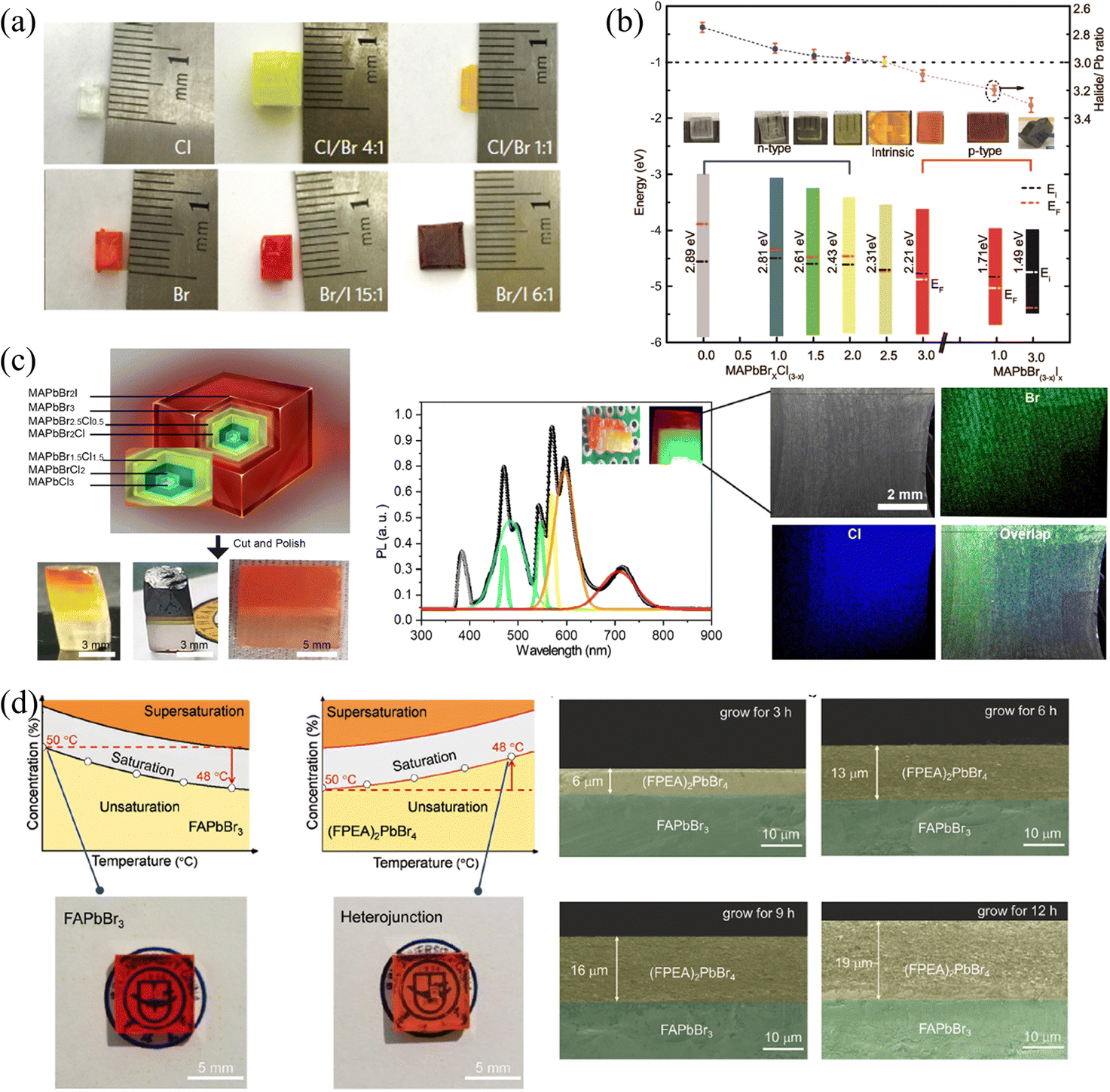 | ||
| Fig. 9 (a) MAPbX3 SCs with different halide components. Reprinted with permission from ref. 31, Copyright 2015, Springer Nature. (b) Halide-to-lead ratio, optical photographs, PN type and band structures of the MAPbX3. (c) Optical photographs of cascade epitaxial SCs, and corresponding PL and EDS spectra. (b) and (c) Reprinted with permission from ref. 38, Copyright 2020, American Chemical Society. (d) Solubility curves and photographs of 3D FAPbBr3 and 2D (FPEA)2PbBr4 SCs, and the thickness of the 3D/2D heterojunction with different reaction times. Reprinted with permission from ref. 80, Copyright 2021, John Wiley and Sons. | ||
Moreover, 2D HP could also be grown outside 3D HP SCs to construct the 2D/3D heterojunctions. Due to the inclusion of longer chains of organic molecules separating the inorganic layers, the structure of 2D HPs has significant differences from 3D HPs. Therefore, the A-site exchange cannot succeed like the X-site halide exchange in the original 3D HP structure, 2D HPs can only be grown by epitaxial growth. Wei and coworkers80 utilized the solution-processed epitaxial method to construct 3D/2D HP SCs heterojunction. Since 2D HPs do not possess inversed solubility like their 3D counterparts, the cooling method was used to grow the 2D (FAPEA2)PbBr4 SC layer outside the 3D FAPbBr3 SC, as shown in Fig. 9d. Owing to the same octahedral [PbBr6]4− sheets of (FAPEA2)PbBr4 and FAPbBr3, the 2D layer is closely epitaxially grown on the surface of 3D SC, and the thickness of the 2D layer linearly increased from 6 to 13 to 19 μm as grown in the saturated solution for 3, 6, and 9 hours, respectively. Unlike the above epitaxial SCs layers, 2D HP layers can also be grown on the surface of SCs by simple liquid immersion81 or spin-coating.24
2.3 Nanowires (microwires)
Nanowires (NWs) and microwires (MWs) can be viewed as another form of SCs; that is, under specific growth conditions and/or induced by external forces, the growth of SCs is promoted only in one dimension, and the size is much larger than that of the other two dimensions. Benefited from the specular one-dimensional (1D) structure, a large compositional gradient can be fabricated in these NWs and MWs to form bandgap-graded 1D structures, which have received ever-increasing interest in multi-color lasers82,83 and multi-wavelength detection and recognition.41 Therefore, this section will introduce the fabrication of halide gradient in these 1D NWs and MWs by different methods, meanwhile, the properties of these gradient NWs and MWs are presented and their advantages and disadvantages are compared in detail.Jin and coworkers77 synthesized bromide-gradient MAPbBrxI3−x NWs by perpendicularly connecting the as-prepared MAPbI3 NWs with bulk MAPbBr3 SCs to realize solid-to-solid ion exchange from one end of pure MAPbI3 NWs (shown in Fig. 10a). To be mentioned, even the ion exchange occurs in these small-sized NWs, where the NWs are about 5–10 micrometers in length and a few hundred nanometers in width, it takes at least 15 days due to the ultra-slow solid-phase ion diffusion. This is also consistent with the previous discussion in the single crystals section that the solid-phase ion exchange is hardly achieved in bulk SCs due to the difficulty of achieving close contact of interfaces and ultra-slow ion diffusion rate between solid phases. After the anion exchange reaction, the NWs removed from SC exhibit a halide gradient and have significantly blue-shifted PL emission at the ion-exchanged end (shown in Fig. 10b).
 | ||
| Fig. 10 (a) Schematic diagram of solid-phase ion exchange for HP NWs. (b) EDS mappings and PL spectra at different regions of compositional gradient MAPbBrxI3−x NWs. (a) and (b) Reprinted with permission from ref. 77, Copyright 2017, American Chemical Society. (c) PL spectra at the end and center of CsPbBrxI3−x NWs at different reaction times, and corresponding confocal laser scanning microscope image and schematic diagram of the growth process of compositional gradient CsPbBrxI3−x NWs. Reprinted with permission from ref. 89, Copyright 2018, John Wiley and Sons. (d) Schematic diagram of the dip-and-pull method for liquid-phase ion exchange for MWs, and corresponding characterization of the compositional gradient MWs. Reprinted with permission from ref. 41, Copyright 2022, John Wiley and Sons. | ||
In addition to the utilization of the source-moving chemical vapor deposition (CVD) method to fabricate compositional gradient NWs like those prepared by the Pan group.84–88 Yan and coworkers89 found that composition-graded CsPbBrxI3−x NWs were spontaneously formed due to the temperature-controlled anion-exchange reaction. Briefly, the quartz boat filled with CsI powder was placed at the center of the heating zone of the CVD system, and the PbBr2 and PbI2 with a molar ratio of 1![[thin space (1/6-em)]](https://www.rsc.org/images/entities/char_2009.gif) :1 were placed in the upper stream. The NWs were reacted in the system with temperature control at 450 °C. The obtained NWs possess an increased Br/I ratio from the center to the ends (shown in Fig. 10c). As the PL peak is composition-dependent, the PL spectra of the as-prepared NWs reacted from 5 min to 40 min exhibited a red shift in the central region, proving that the center is an I-rich region. The corresponding confocal laser scanning microscope images at different reaction times also indicated that the composition of whole NWs transforms from I-rich to Br-rich as the reaction processing with an inhomogeneous I-rich center consistently. The origin of this spontaneous inhomogeneity should be ascribed to the temperature-controlled anion exchange reaction, where if the temperature is higher than 530 °C, homogeneous nanowires are formed.
:1 were placed in the upper stream. The NWs were reacted in the system with temperature control at 450 °C. The obtained NWs possess an increased Br/I ratio from the center to the ends (shown in Fig. 10c). As the PL peak is composition-dependent, the PL spectra of the as-prepared NWs reacted from 5 min to 40 min exhibited a red shift in the central region, proving that the center is an I-rich region. The corresponding confocal laser scanning microscope images at different reaction times also indicated that the composition of whole NWs transforms from I-rich to Br-rich as the reaction processing with an inhomogeneous I-rich center consistently. The origin of this spontaneous inhomogeneity should be ascribed to the temperature-controlled anion exchange reaction, where if the temperature is higher than 530 °C, homogeneous nanowires are formed.
Our group41 proposed halide gradient MWs by dip-and-pull method to achieve liquid-phase ion exchange, which is similar to gradient films fabricated by the dip-and-pull method described above. Firstly, the space-limit solution method to grow PbBr2 MWs was employed. Briefly, the PbBr2 solution was dropped between two glasses to limit the longitudinal growth, and as the DMF solvent slowly volatilized, the one-dimensional PbBr2 MWs were obtained. Then, the as-prepared MABr2 NWs were soaked into MABr/isopropanol (IPA) solution to convert into MAPbBr3 MWs, accompanied by the change of PbBr64− octahedral from edge-sharing mode in PbBr2 to the corner-sharing mode in HPs. Finally, as illustrated in Fig. 10d, the dip-and-pull method was applied for MAPbBr3 MWs. MAPbBr3 MWs were dipped into MAI solution from one end to near the middle, and pulled out after exchanging the MWs for a certain period of time, then this operation was repeated in MACl solution at the other end to manipulate the Cl–Br–I halide exchange. Since the size of the Br− is between that of Cl− and I−, the halide exchange to Cl/I from MAPbBr3 MWs avoids excessive lattice mismatch, avoiding morphology destruction and defect formation. To prevent morphology destruction caused by abrupt halide ion change, the dip-and-pull rate was carefully controlled at 0.5 mm s−1. Thus, the gradient bandgap MAPbX3 MWs was fabricated, and the entire MW exhibits gradient PL peaks ranging from 428 to 758 nm.
2.4 Stability issue
Owing to the inherently soft lattice allowing greater tolerance to lattice mismatch,90 the compositional gradient in HP materials can be constructed in various approaches, and each method has its own advantages and limitations. As summarized above, the comparison of different approaches to realize gradient engineering is listed in Table 1. Nevertheless, the stability of the constructed gradient mainly depends on the specific HP formed rather than the methods. The stability of the compositional gradient requires considering the following aspects. First, the entropy-driven ion movement from the higher concentration to the lower tends to reach concentration equilibrium. Secondly, the ion migration due to lower activation energy may also affect the compositional gradients. In HPs, the migration activation energies are relatively low, taking MAPbI3 as an example, the activation energy of I−, MA+, and Pb2+ vacancies are 0.58, 0.84, and 2.31 eV, respectively.91 Thirdly, external energy such as photoirradiation may cause halogen ions to segregate.92,93| Classification | Ion exchange | Epitaxial methods | Spontaneous gradient | ||||
|---|---|---|---|---|---|---|---|
| Solid-phase | Liquid-phase | Vapor-phase | Deposition | Growth | Anti-solvent | Heteroatoms doping | |
| Speed | Slow | Fast | Medium | Controlled | Slow | Based on methods | |
| Applicability | Polycrystalline films53 | Polycrystalline films58 | NWs (MWs)89 | Sn/Pb gradient films55,56 | Sb, In/Pb gradient films57 | ||
| SCs78 | NWs (MWs)94 | SCs38 | |||||
| NWs (MWs)77 | |||||||
| Operation | Easy | Complicated (compared with ion exchange) | Selective | ||||
| Stability | Depending on the specific HP forms | ||||||
For the stability issue, whether the ion diffusion driven by the different ion concentrations can be effectively suppressed is the key to maintaining the compositional gradient. Taking polycrystalline film as an example, no matter what is the preparation method and chosen improved strategy, there are inevitably many grain boundaries inside it.4 Although defects exist at these grain boundaries to increase the probability of carrier recombination, the grain boundaries also act as barriers to ion diffusion. Thus, the polycrystalline films can exhibit excellent stability of compositional gradient, which tends to be maintained almost indefinitely.53,95 In contrast, the stability of HP films under ambient conditions limits their long-term use since water and oxygen molecules can enter the film along the grain boundaries, destroying the HP structure.96 In order to trade-off between the stability of the gradient and the performance of the films, an appropriate grain size is required. Moreover, the issues of ion migration and halogen ions segregating under external energy can also destabilize gradients in polycrystalline films.91–93
While for HP SCs, the absence of grain boundaries facilitates the transport of externally introduced ions, which is not conducive to maintaining the gradients. Generally, the ion-exchanged compositional gradient would become homogeneous after a few days. However, for the epitaxial method, there is an original interface between epitaxially-grown SCs, and the multi-composition epitaxial SCs, which decreases the concentration gradient between adjacent SCs, slow down the interdiffusion of halogen ions, and improve the stability of compositional gradients for long-term applications.38 Furthermore, the ion migration in HP SCs can be suppressed as a result of the reduction of halogen vacancies.76 It has been reported that the prepared NWs with the compositional gradient present good stability for more than 50 days.77 This phenomenon could be related to the impediment of ion diffusion inside the NWs (which often occurs in polycrystalline films with multiple grain boundaries). This hindrance may originate from the defects inside NWs based on the epitaxial growth of PbAc2 on CH3NH3I isopropanol solution. As hindered by these internal defects, the solid-phase ion exchange from MAPbI3 to MAPbBr3 led to only a blue shift from ∼780 nm to ∼750 nm after 15 days (even if solid-phase ion exchange should be slow). Moreover, the halide gradient is stable from 25 °C to 100 °C, showing great potential for long-term practical applications.
Furthermore, the epitaxial growth of 2D HP nanosheets (microsheets) also provides a new strategy to suppress ion diffusion and consequently improve gradient stability. Dou and coworkers stacked different 2D HP nanosheets (microsheets) layer-by-layer to construct vertical heterostructures by epitaxial growth97 and mechanical exfoliation-assembly.98 Since 2D HPs are composed of organic and inorganic layers periodically repeated along the out-of-plane direction, this quantum well structure can significantly reduce the propagation of ions along the out-of-plane direction. Therefore, it can not only reduce the ion diffusion by introducing a sharp epitaxial interface through the heterogeneous two-layer contact but also further improve the stability of the vertical composition gradient. Even the in-plane ion diffusion in 2D HPs can be inhibited by incorporating rigid π-conjugated organic ligands.97 In view of this, the introduction of 2D HPs can be regarded as a feasible solution to suppress the ion diffusion in the compositional gradient.
3. Application
As introduced in the section above, the compositional gradient can be effectively constructed in different forms of HPs. The gradient bandgap along with the formation of compositional gradient and the heterojunction formed by the connection of different P-type and N-type materials could exhibit improved carrier extraction. Besides, materials with compositional gradients can realize functions based on active layers with different bandgaps in one device, which is conducive to the realization of multi-band detection/emission and integration of the system. In this section, the advanced applications of these compositional gradient HPs and their advantages will be introduced. Besides, the different forms of HPs, their sizes will also play an important role in different application scenarios. We hope that through the systematic review, giving rise to the prosperity of the compositional gradient HPs in solar cells, LEDs, phototransistors and other novel applications.3.1 Enhanced carrier extraction
The continuous band structure formed by the compositional gradient is beneficial to the separation of charge carriers, which can effectively promote the extraction and transport of charge carriers under an applied bias.57 The variation of the halide composition in HPs dominantly affects the valence band maximum that exerts a notable extraction effect on holes. Furthermore, it is of remarkable significance for charge carrier balance to accelerate hole extraction due to the slower mobility of holes than electrons inside HPs.99The tilted valence band of the Br/I gradient gives rise to accelerated hole extraction in HPs films. Meanwhile, Choi and coworkers37 found that carriers in the gradient films (HBr-treated) exhibit a shorter average lifetime (22.85 ns) than that of the reference sample (177.98 ns), and HBr-treated films also present significant PL quenching, as shown in Fig. 11a. These phenomena should be attributed to the more efficient charge injection in HBr-treated, thus the hole extraction to the hole transport layer (HTL) can also be enhanced. As a result of the promoted carrier extraction in the Br/I gradient HP films, the HP solar cells exhibit increased Voc from 1.08 to 1.11 V, and FF from 0.71 to 0.74. Moreover, the long-term stability was dramatically enhanced in the compositional gradient films without a loss of current density. In addition, the prepared films with MA/Sn-rich top and FA/Pb-rich bottom lead to a distribution of bandgap energy, which is characterized by ultraviolet photoelectron spectroscopy (UPS), as shown in Fig. 11b. Therefore, the conduction and valence band energy levels increase as the vertical depth of films increases.56 Thus, the vertical compositional gradient of FA/MA and Pb/Sn in HP phototransistors is beneficial for the separation of photogenerated carriers, thereby enhancing the photogating effect in the HP channel. As a consequence, the maximum gains (G) of the transistor reach about 2 × 10⁵, 1 × 10⁶, and 9 × 10⁴ at 980, 760, and 370 nm illumination, respectively.56
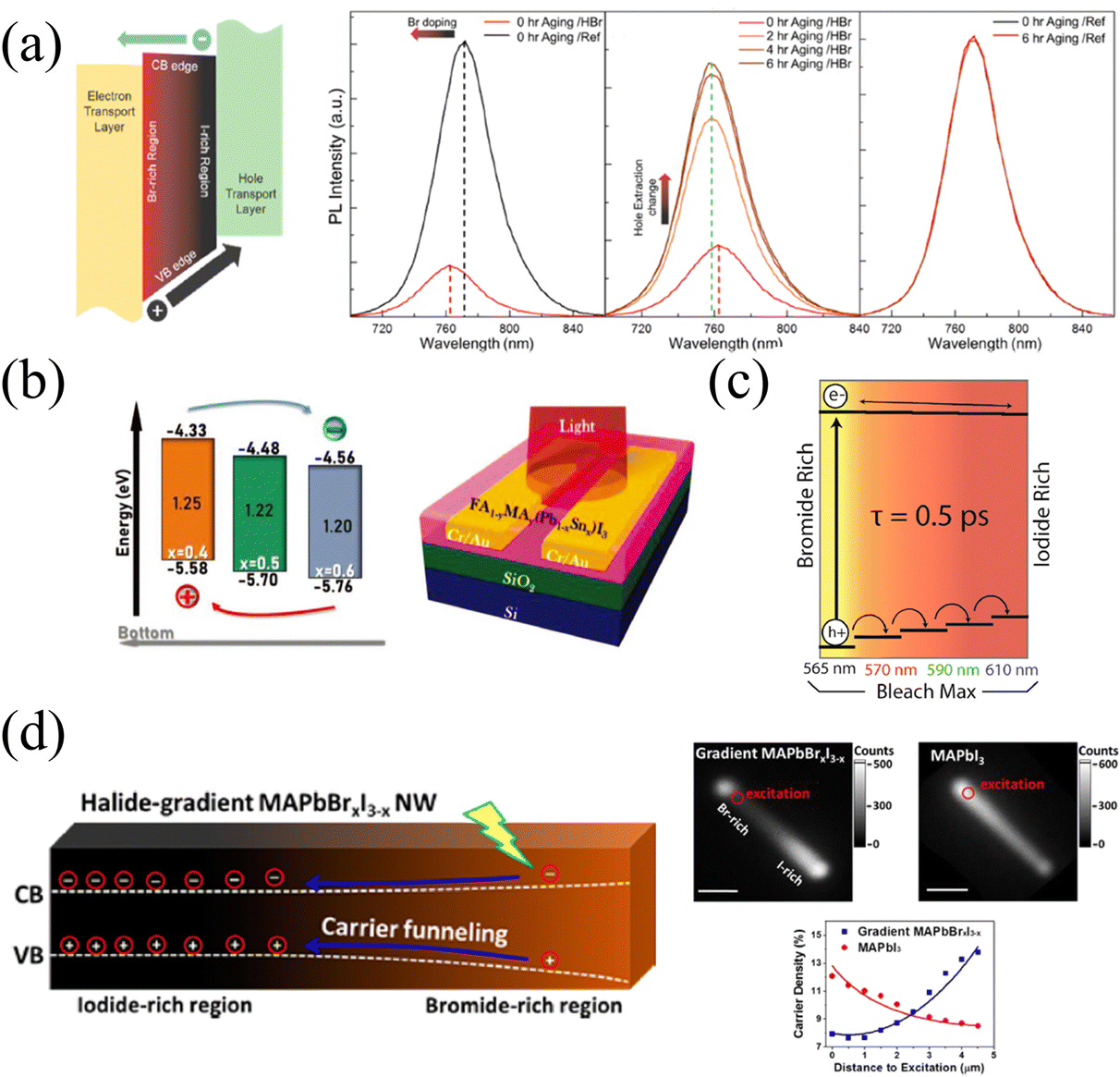 | ||
| Fig. 11 (a) Schematic diagram of the energy band level of compositional gradient HP film, and PL spectra of reference and HBr-treated films before and after aging. Reprinted with permission from ref. 37, Copyright 2016, American Chemical Society. (b) Schematic diagram of the energy band level of Sn/Pb gradient HP film, and corresponding phototransistor structure. Reprinted with permission from ref. 56, Copyright 2022, John Wiley and Sons. (c) Schematic diagram of the energy band level of compositional gradient CsPbBrxI3−x films. Reprinted with permission from ref. 54, Copyright 2016, American Chemical Society. (d) Schematic diagram of the energy band level of compositional gradient MAPbBrxI3−x NW, and corresponding characterization of carrier dynamics. Reprinted with permission from ref. 77, Copyright 2017, American Chemical Society. | ||
This enhanced holes extraction capability also exists in CsPbX3, within the bromine-iodide composition gradient, the valence band maximum shifts to higher energies from the Br-rich region to the I-rich region, facilitating the extraction of holes (shown in Fig. 11c). While electrons are less affected by the compositional gradient as a result of the insignificant change in the conduction band minimum.54,59 Furthermore, owing to the different N- and P-types possessed by HPs with different components, the built-in electric field generated in the PN junction formed by the composition gradient would also increase the injection current under forward bias.38
In addition to the driving force to holes from the Br-rich region to the I-rich region owing to the increased valence band maximum, Jin and coworkers77 also found that the movement of holes pulls the electrons to move together by the Coulomb force in the gradient MAPbBrxI3−x NWs. The unidirectional transportation of charge carriers forms an energy funnel instead of spontaneous carrier diffusion, resulting in carrier flow from the Br-rich region to the I-rich region, which can also be proved by inhomogeneous PL intensity on NWs (due to the recombination of holes and electrons), as illustrated in Fig. 11d. The inhomogeneous PL intensity is proportional to n2, where n represents the carrier density, and the relationship between relative carrier density and distance to the excitation spot along the NWs are opposite in gradient MAPbBrxI3−x and pure MAPbI3 NWs. The carrier transportation carrier movement driven by the energy funnel delivers about 60% of carriers over 2 μm, which is larger than the opposite diffusion caused by the concentration gradient (only 45%), thus resulting in the accumulation of carriers at the iodide-rich region. This effective unidirectional transportation of charge carriers promises great potential in long-distance carrier transportation and energy delivery for efficient LEDs.100
3.2 Multi-spectral recognition
Multi-spectral recognition is the technique of collecting and distinguishing photon signals from two or more frequency ranges and resolving the target spectral composition and proportions, which plays an essential role in the fields of imaging, spectrographic analysis, optical communications, and in situ characterization.53 To parse the spectrum, it is essential to realize narrowed light recognition, which generally requires optical prism or interference/interferometric filters to resolve the wide spectrum into narrow-band light or the integration of narrowband semiconductors. However, the miniaturization and integration of traditional multispectral detectors hamper its development, due to the inability to avoid optical components or rely on multi-detector integration.In light of this, the compositional gradient materials exhibit continuous bandgaps, which can achieve a continuous narrowband response without optical components and can realize multispectral recognition integrated into a single device. Yang and coworker101 achieved spectral recognition by computationally processing the spectral signals of different bandgap detectors on compositional gradient CdSxSe1−x nanowires. However, hindered by the optical bandgap of CdSxSe1−x, the effective recognition range only covered from 512 nm to 712 nm. While for HPs, the continuously tunable bandgap from UV to NIR accompanied by facial processed compositional gradient provides an outstanding platform for multispectral recognition. Sun et al.62 reported filter-free photodetector arrays based on compositional gradient HP film to realize color discrimination in the visible spectrum, as illustrated in Fig. 12a. On the as-prepared compositional gradient HPs film, they selected active layer regions with suitable bandgaps to build a detector array, that included units that responded only to blue light, to blue and green light, and to the full band. For color discrimination, the blue light information can be obtained from the unit that only responds to blue light, and the green light can be obtained by subtracting the blue light information from the unit that only responded to blue and green light, while the information of red light can be acquired in the same way (Fig. 12b). Furthermore, the light intensity can be calculated according to the relationship between current and light intensity, because the detection units on the device show high linearity for red, green, and blue light, reaching 106, 102, and 96 dB, respectively.
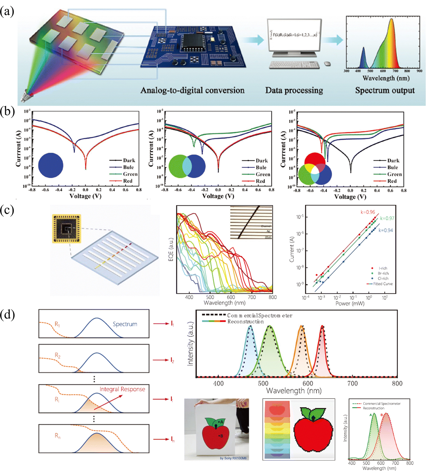 | ||
| Fig. 12 (a) Schematic diagram of the multi-spectral recognition system based on compositional gradient film. (b) I–V curves of detection units based on the absorbers with specific bandgaps under blue, green, and red light illumination. (a) and (b) Reprinted with permission from ref. 62, Copyright 2020, John Wiley and Sons. (c) Schematic diagram, EQE curves and high LDR of the multi-spectral recognition system based on single compositional gradient MW. (d) Multi-spectral recognition and imaging of the incident spectra based on single compositional gradient MW. (c) and (d) Reprinted with permission from ref. 41, Copyright 2022, John Wiley and Sons. | ||
Our group41 also achieved multispectral recognition based on compositional gradient MWs with the algorithm for computational spectral recognition. As shown in Fig. 12c, 30 μm channel Ag electrodes were constructed along the axial direction on the MAPbX3 MWs, where the MW is about 4 mm in length and 21 sensing units were fabricated on it. The responded EQE edge of these photodetectors gradually varies from 450 to 790 nm, as the component changes from MAPbCl3 to MAPbI3, with a responsivity of over 20 mA W−1. Meanwhile, the linear dynamic range (LDR) reached 59, 66, and 68 dB for the Cl-rich, Br-rich, and I-rich parts, respectively. These laudable detection parameters set the precondition for further computational spectral recognition. The algorithm for computational spectral recognition was proposed to realize multi-spectral recognition. Briefly, the photocurrent (Ii) of the detector unit should be the product of the response function Ri(λ) and the incident spectrum is F(λ) is expressed as
 | (1) |
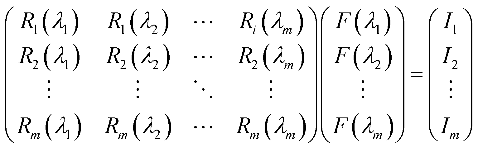 | (2) |
To simplify the computational process, the unknown function F(λ) was viewed as a linear combination of a series of Gaussian basis functions ϕj(λ)
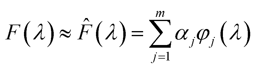 | (3) |
| Aα = c | (4) |
3.2 Multi-color emission
Laser stands for light amplification by stimulated emission of radiation, in which three unavoidable elements are required: gain medium, resonant cavity, and pumping source.82 Under the excitation of the pump source, the particles (atoms, molecules, ions, or carriers) realize the transition from the ground state to the excited state and achieve a population inversion. The particles at the excited state will return to the ground state under the excitation of the photon with proper energy, and release a photon perfectly identical to the excited photon. The resonant cavity imposes a limit on the transmission of generated photons. If the optical gain is greater than the optical loss and exceeds the threshold, the unidirectional high-intensity laser will release. Great progress in lasers has been reported based on the compositional gradient NWs.84–88 Since the use of low-dimensional nanostructures (such as NWs, nanorods, or nanosheets) as resonators can not only obtain low-threshold and high cavity quality factor (Q) but also realize the miniaturization of lasers. Moreover, the compositional gradient exhibits varying bandgaps on a single semiconductor, enabling dual-color or multi-color lasers to cover broadband spectra. The dual-color or multi-color lasers have profound potential in displays, chemical, biological sensing, optical communication, etc.,82 especially compared to LEDs, white light produced by multi-color lasers has a higher output power owing to the higher energy conversion efficiencies.Yan and coworkers89 proposed a dual-color laser based on the composition-graded CsPbBrxI3−x NWs. As shown in Fig. 13a, the position-dependent PL is presented, which essentially comes from the graded bandgaps, setting the precondition for realizing more than one color lasing under single excitation. As excited by a pulsed 400 nm laser with the excitation intensity exceeding the threshold focused at the diameter of NWs, the PL spectra across the NW were collected, where the bromine content decreases continuously from region A to C. It is worth mentioning that multi-mode lasing around 521 and 556 nm (which are detected in regions A and C, respectively) are collected in region B, which possesses the intermediate composition, as shown in Fig. 13b. The pumping fluence-dependent PL spectra indicate that with the pumping fluence lower than 8.1 μJ cm−2, the PL located at 534 nm is consistent with that under continuous laser excitation. While the pumping fluence (18 μJ cm−2) is greater than the threshold of cyan light, PL around 521 nm can be observed, and if it is greater than the threshold of both cyan and green light, the B region exhibits dual-color lasing of both 521 and 556 nm. The corresponding integrated intensity of the lasing peak at the cyan and green bands of region B versus pumping fluence also illustrates the above process. This result proves the dual-color lasing with a wavelength separation of 35 nm in the composition-graded CsPbBrxI3−x NWs, which provides a promising application strategy for compositional gradient HPs, especially HPs with nanostructures as gain media.
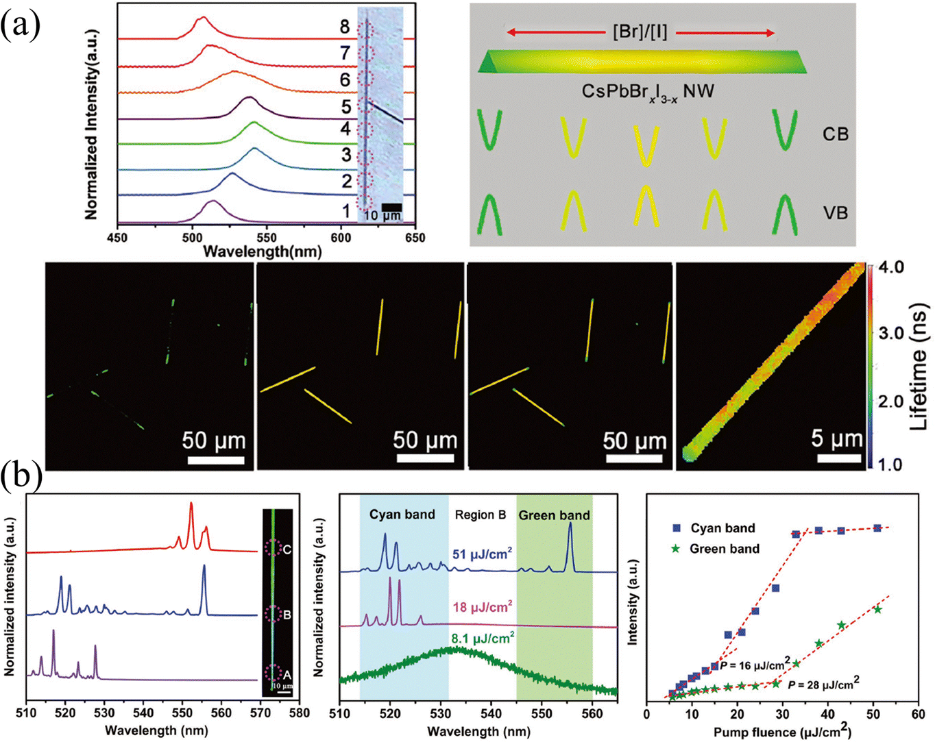 | ||
| Fig. 13 (a) Position-dependent PL spectra, schematic diagram of the energy band level, confocal laser scanning microscope image and fluorescence lifetime imaging microscope images of CsPbBrxI3−x NW. (b) Characterization of the dual-color lasing in the compositional gradient CsPbBrxI3−x NW. (a) and (b) Reprinted with permission from ref. 89, Copyright 2018, John Wiley and Sons. | ||
While for HPs-based LEDs, thanks to the tunable emission over the entire visible spectrum with a narrow bandwidth (<20 nm) and high photoluminescence quantum yield, HPs have garnered extreme interest as an ideal candidate for next-generation LED material.102 Despite remarkable progress in specific wavelength LEDs,16–19 the integration of multi-color and even white light emission is of significant importance. However, the active layer of LEDs needs to be sandwiched by the hole transport layer and the electron transport layer, thus direct utilization of single material with different bandgaps such as multi-color lasers is not feasible. Taking multi-color single-chip white LED as an example, the cascaded GaAs/GaN devices are separately sandwiched by respective N-doped and P-doped layers.103 However, it is attainable to introduce heterophase gradients in the active layer, e.g., α/δ-CsPbI3104 and CsPbBr3/Cs4PbBr6105 as the active layer to realize multi-color emission, which can be attributed to the charge transfer and balanced radiative recombination between the heterophases and introduced radiative defects, respectively. Moreover, the blue-green-red emitting HPs based on CsPbCl0.5/Br0.5, CsPbBr3, and CsPbBr0.4/I0.6 films can be integrated as an efficient UV to visible color converting material for multi-color emission.40
4. Conclusions
In this review, a series of composition gradient preparation methods for different forms of HPs are overviewed. According to the dimension or macroscopic form, HPs are divided into polycrystalline films, single crystals, and nanowires (microwires). It is worth mentioning that although 0-dimensional quantum dots (QDs) can change different components through ion exchange, they still need to be spin-coated to form gradients as polycrystalline films, thus the gradient preparation method is almost consistent with the polycrystalline films. Except for some methods that use an anti-solvent or doping ion size to induce spontaneous gradient formation, most gradient construction methods utilize ion exchange, which can be further divided into solid-, liquid-, and vapor-phase ion exchange. Among them, the solid-phase ion exchange is limited by the slow ion diffusion effect between solid phases, as well as the discontinuity of the interfaces, so external pressure and high temperature are required to accelerate the ion exchange. In contrast, liquid-phase and vapor-phase ion exchange have a faster exchange rate, and it needs to be considered that while achieving composition exchange, the exchanged ion will not diffuse too quickly throughout the entire material so that the overall composition changes. Furthermore, owing to the different ion concentrations between the gradients, the entropy-driven ion diffusion will reduce the gradient concentration and eventually favor a uniform composition. It is found that compared with polycrystalline films containing many grain boundaries (which hinder the diffusion of ions), ion-exchange gradients in SCs and SC-like nanowires (microwires) would be fully diffused evenly within a few weeks, associated with the ambient temperature and concentration gradient. This suggests that the stability of the gradient is of great importance as the gradient construction.Since the changes in the HP component (especially X-site halogen ions) can significantly affect the semiconductor bandgaps, the compositional gradient leads to a continuous change in the bandgap. For example, in the Br/I gradient, the valence band maximum increases as the I ratio increases, which is beneficial to the transport of holes, and finally improve the extraction efficiency of holes in optoelectronic devices. More importantly, the compositional gradient HPs can realize the integration of active layers with multiple bandgaps, which have profound implications in the integration and miniaturization of multi-spectral detection/recognition, and the emission of multi-color light. It is expected that this review can provide guidance for the further development of gradient HPs and their applications.
Conflicts of interest
There are no conflicts to declare.Acknowledgements
We acknowledge the financial support by the National Natural Science Foundation of China (No. 52172146), Natural Science Foundation of Jiangsu Province (BK20190443 and BK20200071), Shuangchuang Talent of Jiangsu Province (No. JSSCRC2021506).References
- Q. Jiang, J. Tong, R. A. Scheidt, X. Wang, A. E. Louks, Y. Xian, R. Tirawat, A. F. Palmstrom, M. P. Hautzinger, S. P. Harvey, S. Johnston, L. T. Schelhas, B. W. Larson, E. L. Warren, M. C. Beard, J. J. Berry, Y. Yan and K. Zhu, Science, 2022, 378, 1295–1300 CrossRef CAS PubMed
.
- C. Li, X. Wang, E. Bi, F. Jiang, S. M. Park, Y. Li, L. Chen, Z. Wang, L. Zeng, H. Chen, Y. Liu, C. R. Grice, A. Abudulimu, J. Chung, Y. Xian, T. Zhu, H. Lai, B. Chen, R. J. Ellingson, F. Fu, D. S. Ginger, Z. Song, E. H. Sargent and Y. Yan, Science, 2023, 379, 690–694 CrossRef CAS PubMed
- J. Park, J. Kim, H. S. Yun, M. J. Paik, E. Noh, H. J. Mun, M. G. Kim, T. J. Shin and S. I. Seok, Nature, 2023 DOI:10.1038/s41586-023-05825-y
- T. Yang, L. Gao, J. Lu, C. Ma, Y. Du, P. Wang, Z. Ding, S. Wang, P. Xu, D. Liu, H. Li, X. Chang, J. Fang, W. Tian, Y. Yang, S. F. Liu and K. Zhao, Nat. Commun., 2023, 14, 839 CrossRef CAS PubMed
- F. Cao, J. Chen, D. Yu, S. Wang, X. Xu, J. Liu, Z. Han, B. Huang, Y. Cu, K. L. Choy and H. Zeng, Adv. Mater., 2020, 32, 1905362 CrossRef CAS PubMed
- J. Feng, APL Mater., 2014, 2, 081801 CrossRef
- Y. Zhang, Y. Liu, Y. Li, Z. Yang and S. Liu, J. Mater. Chem. C, 2016, 4, 9172–9178 RSC
- K. Zheng, Q. Zhu, M. Abdellah, M. E. Messing, W. Zhang, A. Generalov, Y. Niu, L. Ribaud, S. E. Canton and T. Pullerits, J. Phys. Chem. Lett., 2015, 6, 2969–2975 CrossRef CAS PubMed
- W.-J. Yin, T. Shi and Y. Yan, Appl. Phys. Lett., 2014, 104, 063903 CrossRef
- J. S. Manser, J. A. Christians and P. V. Kamat, Chem. Rev., 2016, 116, 12956–13008 CrossRef CAS PubMed
- F. Cao, D. Yu, W. Ma, X. Xu, B. Cai, Y. M. Yang, S. Liu, L. He, Y. Ke, S. Lan, K.-L. Choy and H. Zeng, ACS Nano, 2020, 14, 5183–5193 CrossRef CAS PubMed
- S. Yakunin, D. N. Dirin, Y. Shynkarenko, V. Morad, I. Cherniukh, O. Nazarenko, D. Kreil, T. Nauser and M. V. Kovalenko, Nat. Photonics, 2016, 10, 585–589 CrossRef CAS
- Z. Song, C. L. McElvany, A. B. Phillips, I. Celik, P. W. Krantz, S. C. Watthage, G. K. Liyanage, D. Apul and M. J. Heben, Energy Environ.
Sci., 2017, 10, 1297–1305 RSC
- M. Cai, Y. Wu, H. Chen, X. Yang, Y. Qiang and L. Han, Adv. Sci., 2017, 4, 1600269 CrossRef PubMed
- A. Kojima, K. Teshima, Y. Shirai and T. Miyasaka, J. Am. Chem. Soc., 2009, 131, 6050–6051 CrossRef CAS PubMed
- S. Liu, Z. Guo, X. Wu, X. Liu, Z. Huang, L. Li, J. Zhang, H. Zhou, L. D. Sun and C. H. Yan, Adv. Mater., 2023, 35, 2208078 CrossRef CAS PubMed
- J. S. Kim, J. M. Heo, G. S. Park, S. J. Woo, C. Cho, H. J. Yun, D. H. Kim, J. Park, S. C. Lee, S. H. Park, E. Yoon, N. C. Greenham and T. W. Lee, Nature, 2022, 611, 688–694 CrossRef CAS PubMed
- J. Jiang, Z. Chu, Z. Yin, J. Li, Y. Yang, J. Chen, J. Wu, J. You and X. Zhang, Adv. Mater., 2022, 34, 2204460 CrossRef CAS PubMed
- Y. Sun, L. Ge, L. Dai, C. Cho, J. Ferrer Orri, K. Ji, S. J. Zelewski, Y. Liu, A. J. Mirabelli, Y. Zhang, J. Y. Huang, Y. Wang, K. Gong, M. C. Lai, L. Zhang, D. Yang, J. Lin, E. M. Tennyson, C. Ducati, S. D. Stranks, L. S. Cui and N. C. Greenham, Nature, 2023, 615, 830–835 CrossRef CAS PubMed
- S. Yakunin, M. Sytnyk, D. Kriegner, S. Shrestha, M. Richter, G. J. Matt, H. Azimi, C. J. Brabec, J. Stangl, M. V. Kovalenko and W. Heiss, Nat. Photonics, 2015, 9, 444–449 CrossRef CAS PubMed
- D. Yu, P. Wang, F. Cao, Y. Gu, J. Liu, Z. Han, B. Huang, Y. Zou, X. Xu and H. Zeng, Nat. Commun., 2020, 11, 3395 CrossRef CAS PubMed
- H. Wei, D. DeSantis, W. Wei, Y. Deng, D. Guo, T. J. Savenije, L. Cao and J. Huang, Nat. Mater., 2017, 16, 826–833 CrossRef CAS PubMed
- Z. Han, W. Fu, Y. Zou, Y. Gu, J. Liu, B. Huang, D. Yu, F. Cao, X. Li, X. Xu and H. Zeng, Adv. Mater., 2021, 33, 2003852 CrossRef CAS PubMed
- J. Li, Y. Zou, D. Hu, Y. Gu, Z. Han, J. Liu and X. Xu, Nanoscale, 2022, 14, 6109–6117 RSC
- S. Jin, ACS Energy Lett., 2021, 6, 3386–3389 CrossRef CAS
- L. N. Quan, B. P. Rand, R. H. Friend, S. G. Mhaisalkar, T. W. Lee and E. H. Sargent, Chem. Rev., 2019, 119, 7444–7477 CrossRef CAS PubMed
- Z. Shi, Y. Zhang, C. Cui, B. Li, W. Zhou, Z. Ning and Q. Mi, Adv. Mater., 2017, 29, 1701656 CrossRef PubMed
- A. D. Wright, C. Verdi, R. L. Milot, G. E. Eperon, M. A. Perez-Osorio, H. J. Snaith, F. Giustino, M. B. Johnston and L. M. Herz, Nat. Commun., 2016, 7, 11755 CrossRef PubMed
- N. J. Jeon, J. H. Noh, W. S. Yang, Y. C. Kim, S. Ryu, J. Seo and S. I. Seok, Nature, 2015, 517, 476–480 CrossRef CAS PubMed
- T. Chiba, Y. Hayashi, H. Ebe, K. Hoshi, J. Sato, S. Sato, Y.-J. Pu, S. Ohisa and J. Kido, Nat. Photonics, 2018, 12, 681–687 CrossRef CAS
- Y. Fang, Q. Dong, Y. Shao, Y. Yuan and J. Huang, Nat. Photonics, 2015, 9, 679–686 CrossRef CAS
- H. Min, D. Y. Lee, J. Kim, G. Kim, K. S. Lee, J. Kim, M. J. Paik, Y. K. Kim, K. S. Kim, M. G. Kim, T. J. Shin and S. Il Seok, Nature, 2021, 598, 444–450 CrossRef CAS PubMed
- L. Zhao, Y. Zhou, Z. Shi, Z. Ni, M. Wang, Y. Liu and J. Huang, Nat. Photonics, 2023, 17, 315–323 CrossRef CAS
- W. Tang, J. Zhang, S. Ratnasingham, F. Liscio, K. Chen, T. Liu, K. Wan, E. S. Galindez, E. Bilotti, M. Reece, M. Baxendale, S. Milita, M. A. McLachlan, L. Su and O. Fenwick, J. Mater. Chem. A, 2020, 8, 13594–13599 RSC
- R. Meng, G. Wu, J. Zhou, H. Zhou, H. Fang, M. A. Loi and Y. Zhang, Chem. – Eur. J., 2019, 25, 5480–5488 CrossRef CAS PubMed
- Y. Liu, Z. Yang, D. Cui, X. Ren, J. Sun, X. Liu, J. Zhang, Q. Wei, H. Fan, F. Yu, X. Zhang, C. Zhao and S. F. Liu, Adv. Mater., 2015, 27, 5176–5183 CrossRef CAS PubMed
- M. C. Kim, B. J. Kim, D. Y. Son, N. G. Park, H. S. Jung and M. Choi, Nano Lett., 2016, 16, 5756–5763 CrossRef CAS PubMed
- X. Wang, Y. Li, Y. Xu, Y. Pan, C. Zhu, D. Zhu, Y. Wu, G. Li, Q. Zhang, Q. Li, X. Zhang, J. Wu, J. Chen and W. Lei, Chem. Mater., 2020, 32, 4973–4983 CrossRef CAS
- T. Zhang, M. Long, M. Qin, X. Lu, S. Chen, F. Xie, L. Gong, J. Chen, M. Chu, Q. Miao, Z. Chen, W. Xu, P. Liu, W. Xie and J.-B. Xu, Joule, 2018, 2, 2706–2721 CrossRef CAS
- V. Naresh, B. H. Kim and N. Lee, Nano Res., 2020, 14, 1187–1194 CrossRef
- X. Xu, Z. Han, Y. Zou, J. Li, Y. Gu, D. Hu, Y. He, J. Liu, D. Yu, F. Cao and H. Zeng, Adv. Mater., 2022, 34, 2108408 CrossRef CAS PubMed
- G. Kim, S. An, S. K. Hyeong, S. K. Lee, M. Kim and N. Shin, Small, 2021, 17, 2006737 CrossRef CAS PubMed
- H. Jiang, S. Cui, Y. Chen and H. Zhong, Nano Select, 2021, 2, 2040–2060 CrossRef CAS
- K. Sandeep, K. Padmakumar, K. U. Ambili, P. Jishnu, K. H. Fousia, A. R. Ramesh, J. P. Rappai, V. Santhi and M. Shanthil, Phys. Status Solidi B, 2022, 259, 2100600 CrossRef CAS
- J. X. Zhong, W. Q. Wu, L. Ding and D. B. Kuang, Energy Environ. Mater., 2020, 4, 277–283 CrossRef
- S. Moradi, S. Kundu, M. Rezazadeh, V. Yeddu, O. Voznyy and M. I. Saidaminov, Commun. Mater., 2022, 3, 13 CrossRef CAS
- B. Suarez, V. Gonzalez-Pedro, T. S. Ripolles, R. S. Sanchez, L. Otero and I. Mora-Sero, J. Phys. Chem. Lett., 2014, 5, 1628–1635 CrossRef CAS PubMed
- S. Ryu, J. H. Noh, N. J. Jeon, Y. Chan Kim, W. S. Yang, J. Seo and S. I. Seok, Energy Environ. Sci., 2014, 7, 2614–2618 RSC
- F. Hao, C. C. Stoumpos, D. H. Cao, R. P. H. Chang and M. G. Kanatzidis, Nat. Photonics, 2014, 8, 489–494 CrossRef CAS
- J. Liu, Y. Zou, B. Huang, Y. Gu, Y. Yang, Z. Han, Y. Zhang, X. Xu and H. Zeng, Nanoscale, 2020, 12, 20386–20395 RSC
- T. Elmelund, R. A. Scheidt, B. Seger and P. V. Kamat, ACS Energy Lett., 2019, 4, 1961–1969 CrossRef CAS
- Y. Liu, F. Li, Q. Li, K. Yang, T. Guo, X. Li and H. Zeng, ACS Photonics, 2018, 5, 4504–4512 CrossRef CAS
- M. N. Zhang, X. Wu, A. Riaud, X. L. Wang, F. Xie, W. J. Liu, Y. Mei, D. W. Zhang and S. J. Ding, Light: Sci. Appl., 2020, 9, 162 CrossRef CAS PubMed
- J. B. Hoffman, A. L. Schleper and P. V. Kamat, J. Am. Chem. Soc., 2016, 138, 8603–8611 CrossRef CAS PubMed
- J. Cao, H. L. Loi, Y. Xu, X. Guo, N. Wang, C. K. Liu, T. Wang, H. Cheng, Y. Zhu, M. G. Li, W. Y. Wong and F. Yan, Adv. Mater., 2022, 34, 2107729 CrossRef CAS PubMed
- H. L. Loi, J. Cao, C. K. Liu, Y. Xu, M. G. Li and F. Yan, Small, 2023, 19, 2205976 CrossRef CAS PubMed
- H. W. Qiao, S. Yang, Y. Wang, X. Chen, T. Y. Wen, L. J. Tang, Q. Cheng, Y. Hou, H. Zhao and H. G. Yang, Adv. Mater., 2019, 31, 1804217 CrossRef PubMed
- J. Yan, X. Song, Y. Chen and Y. Zhang, Opt. Mater., 2020, 99, 109513 CrossRef CAS
- G. Tong, H. Li, G. Li, T. Zhang, C. Li, L. Yu, J. Xu, Y. Jiang, Y. Shi and K. Chen, Nano Energy, 2018, 48, 536–542 CrossRef CAS
- G. Lu, Z. Chen, Z. Fang, H. Li, Y. Gao, C. Lin, X. Dai, Z. Ye and H. He, Small, 2021, 17, 2103169 CrossRef CAS PubMed
- G. Cen, Y. Xia, C. Zhao, Y. Fu, Y. An, Y. Yuan, T. Shi and W. Mai, Small, 2020, 16, 2005226 CrossRef CAS PubMed
- H. Sun, W. Tian, X. Wang, K. Deng, J. Xiong and L. Li, Adv. Mater., 2020, 32, 1908108 CrossRef CAS PubMed
- H. Sun, K. Deng, Y. Zhu, M. Liao, J. Xiong, Y. Li and L. Li, Adv. Mater., 2018, 30, 1801935 CrossRef PubMed
- J. Xu, Y.-B. Tang, X. Chen, C.-Y. Luan, W.-F. Zhang, J. A. Zapien, W.-J. Zhang, H.-L. Kwong, X.-M. Meng, S.-T. Lee and C.-S. Lee, Adv. Funct. Mater., 2010, 20, 4190–4195 CrossRef CAS
- Y. Sheng, Y. Zha, X. Feng, F. Xing, Y. Di, C. Liu, X. Zhang and Z. Gan, Adv. Opt. Mater., 2023, 11, 2202230 CrossRef CAS
- Q. Dong, Y. Fang, Y. Shao, P. Mulligan, J. Qiu, L. Cao and J. Huang, Science, 2015, 347, 967–970 CrossRef CAS PubMed
- Y. Dang, Y. Liu, Y. Sun, D. Yuan, X. Liu, W. Lu, G. Liu, H. Xia and X. Tao, CrystEngComm, 2015, 17, 665–670 RSC
- J. M. Kadro, K. Nonomura, D. Gachet, M. Gratzel and A. Hagfeldt, Sci. Rep., 2015, 5, 11654 CrossRef PubMed
- D. Shi, V. Adinolfi, R. Comin, M. Yuan, E. Alarousu, A. Buin, Y. Chen, S. Hoogland, A. Rothenberger, K. Katsiev, Y. Losovyj, X. Zhang, P. A. Dowben, O. F. Mohammed, E. H. Sargent and O. M. Bakr, Science, 2015, 347, 519–522 CrossRef CAS PubMed
- M. I. Saidaminov, A. L. Abdelhady, B. Murali, E. Alarousu, V. M. Burlakov, W. Peng, I. Dursun, L. Wang, Y. He, G. Maculan, A. Goriely, T. Wu, O. F. Mohammed and O. M. Bakr, Nat. Commun., 2015, 6, 7586 CrossRef PubMed
- Y. Yang, Y. Yan, M. Yang, S. Choi, K. Zhu, J. M. Luther and M. C. Beard, Nat. Commun., 2015, 6, 7961 CrossRef CAS PubMed
- J. T. Tisdale and T. Smith, CrystEngComm, 2018, 20, 7818–7825 RSC
- Z. Lian, Q. Yan, T. Gao, J. Ding, Q. Lv, C. Ning, Q. Li and J. L. Sun, J. Am. Chem. Soc., 2016, 138, 9409–9412 CrossRef CAS PubMed
- A. A. Zhumekenov, M. I. Saidaminov, M. A. Haque, E. Alarousu, S. P. Sarmah, B. Murali, I. Dursun, X.-H. Miao, A. L. Abdelhady, T. Wu, O. F. Mohammed and O. M. Bakr, ACS Energy Lett., 2016, 1, 32–37 CrossRef CAS
- X. Gong, Z. Huang, R. Sabatini, C. S. Tan, G. Bappi, G. Walters, A. Proppe, M. I. Saidaminov, O. Voznyy, S. O. Kelley and E. H. Sargent, Nat. Commun., 2019, 10, 1591 CrossRef PubMed
- X. Wang, Y. Li, Y. Xu, Y. Pan, Y. Wu, G. Li, Q. Huang, Q. Zhang, Q. Li, X. Zhang, J. Chen and W. Lei, Phys. Status Solidi B, 2020, 257, 1900784 CrossRef CAS
- W. Tian, J. Leng, C. Zhao and S. Jin, J. Am. Chem. Soc., 2017, 139, 579–582 CrossRef CAS PubMed
- N. T. Shewmon, H. Yu, I. Constantinou, E. Klump and F. So, ACS Appl. Mater. Interfaces, 2016, 8, 33273–33279 CrossRef CAS PubMed
- Q. Huang, Z. Li, X. Chen, Y. Xia, Z. Zheng, A. Mei, K. Zhu, Y. Hu, T. Wang, Y. Rong and H. Han, Chem. Commun., 2021, 57, 6125–6128 RSC
- Y. He, W. Pan, C. Guo, H. Zhang, H. Wei and B. Yang, Adv. Funct. Mater., 2021, 21, 2104880 CrossRef
- X. Li, H. Li, W. Bi, Y. Song, C. Ge, A. Wang, Z. Wang, M. Hao, Y. Kang, Y. Yang and Q. Dong, Small, 2022, 18, 2107915 CrossRef CAS PubMed
- X. Zhuang, Y. Ouyang, X. Wang and A. Pan, Adv. Opt. Mater., 2019, 7, 1900071 CrossRef
- H. Li, X. Wang, X. Zhu, X. Duan and A. Pan, Chem. Soc. Rev., 2018, 47, 7504–7521 RSC
- F. Gu, Z. Yang, H. Yu, J. Xu, P. Wang, L. Tong and A. Pan, J. Am. Chem. Soc., 2011, 133, 2037–2039 CrossRef CAS PubMed
- J. Xu, X. Zhuang, P. Guo, Q. Zhang, W. Huang, Q. Wan, W. Hu, X. Wang, X. Zhu, C. Fan, Z. Yang, L. Tong, X. Duan and A. Pan, Nano Lett., 2012, 12, 5003–5007 CrossRef CAS PubMed
- Z. Yang, J. Xu, P. Wang, X. Zhuang, A. Pan and L. Tong, Nano Lett., 2011, 11, 5085–5089 CrossRef CAS PubMed
- A. Pan, W. Zhou, E. S. Leong, R. Liu, A. H. Chin, B. Zou and C. Z. Ning, Nano Lett., 2009, 9, 784–788 CrossRef CAS PubMed
- J. Xu, X. Zhuang, P. Guo, W. Huang, W. Hu, Q. Zhang, Q. Wan, X. Zhu, Z. Yang, L. Tong, X. Duan and A. Pan, Sci. Rep., 2012, 2, 820 CrossRef PubMed
- L. Huang, Q. Gao, L. D. Sun, H. Dong, S. Shi, T. Cai, Q. Liao and C. H. Yan, Adv. Mater., 2018, 30, 1800596 CrossRef PubMed
- H. J. Snaith, Nat. Mater., 2018, 17, 372–376 CrossRef CAS PubMed
- C. Eames, J. M. Frost, P. R. Barnes, B. C. O'Regan, A. Walsh and M. S. Islam, Nat. Commun., 2015, 6, 7497 CrossRef CAS PubMed
- S. J. Yoon, S. Draguta, J. S. Manser, O. Sharia, W. F. Schneider, M. Kuno and P. V. Kamat, ACS Energy Lett., 2016, 1, 290–296 CrossRef CAS
- E. T. Hoke, D. J. Slotcavage, E. R. Dohner, A. R. Bowring, H. I. Karunadasa and M. D. McGehee, Chem. Sci., 2015, 6, 613–617 RSC
- M. M. W. Iqbal, Q. Xie, M. Cai, X. Zou, Q. Zhang, R. Zeng, B. Zou, L. Liao and Q. Wan, Appl. Surf. Sci., 2023, 617, 156458 CrossRef CAS
- S. Jeon, S. Y. Lee, S. K. Kim, W. Kim, T. Park, J. Bang, J. Ahn, H. K. Woo, J. Y. Chae, T. Paik, T. Y. Seong and S. J. Oh, Adv. Opt. Mater., 2020, 8, 2000501 CrossRef CAS
- Q. Wang, B. Chen, Y. Liu, Y. Deng, Y. Bai, Q. Dong and J. Huang, Energy Environ. Sci., 2017, 10, 516–522 RSC
- E. Shi, B. Yuan, S. B. Shiring, Y. Gao, Akriti, Y. Guo, C. Su, M. Lai, P. Yang, J. Kong, B. M. Savoie, Y. Yu and L. Dou, Nature, 2020, 580, 614–620 CrossRef CAS PubMed
- Akriti, E. Shi, S. B. Shiring, J. Yang, C. L. Atencio-Martinez, B. Yuan, X. Hu, Y. Gao, B. P. Finkenauer, A. J. Pistone, Y. Yu, P. Liao, B. M. Savoie and L. Dou, Nat. Nanotechnol., 2021, 16, 584–591 CrossRef CAS PubMed
- X. Y. Chin, D. Cortecchia, J. Yin, A. Bruno and C. Soci, Nat. Commun., 2015, 6, 7383 CrossRef CAS PubMed
- M. Yuan, L. N. Quan, R. Comin, G. Walters, R. Sabatini, O. Voznyy, S. Hoogland, Y. Zhao, E. M. Beauregard, P. Kanjanaboos, Z. Lu, D. H. Kim and E. H. Sargent, Nat. Nanotechnol., 2016, 11, 872–877 CrossRef CAS PubMed
- Z. Yang, T. Albrow-Owen, H. Cui, J. Alexander-Webber, F. Gu, X. Wang, T.-C. Wu, M. Zhuge, C. Williams, P. Wang, A. V. Zayats, W. Cai, L. Dai, S. Hofmann, M. Overend, L. Tong, Q. Yang, Z. Sun and T. Hasan, Science, 2019, 365, 1017–1020 CrossRef CAS PubMed
- J. Chen, H. Xiang, J. Wang, R. Wang, Y. Li, Q. Shan, X. Xu, Y. Dong, C. Wei and H. Zeng, ACS Nano, 2021, 15, 17150–17174 CrossRef CAS PubMed
- X. Guo, G. D. Shen, B. L. Guan, X. L. Gu, D. Wu and Y. B. Li, Appl. Phys. Lett., 2008, 92, 013507 CrossRef
- J. Chen, J. Wang, X. Xu, J. Li, J. Song, S. Lan, S. Liu, B. Cai, B. Han, J. T. Precht, D. Ginger and H. Zeng, Nat. Photonics, 2020, 15, 238–244 CrossRef
- K. Ma, Q. Gui, C. Liu, Y. Yang, F. Xing, Y. Di, X. Wen, B. Jia and Z. Gan, Research, 2022, 2022, 9896548 CAS
| This journal is © The Royal Society of Chemistry 2023 |