 Open Access Article
Can ferroelectric polarization explain the high performance of hybrid halide perovskite solar cells?†
Tejas S.
Sherkar
* and
L.
Jan Anton Koster
Zernike Institute for Advanced Materials, University of Groningen, Nijenborgh 4, 9747AG, Groningen, The Netherlands. E-mail: t.sherkar@rug.nl
First published on 23rd November 2015
Abstract
The power conversion efficiency of photovoltaic cells based on the use of hybrid halide perovskites, CH3NH3PbX3 (X = Cl, Br, I), now exceeds 20%. Recently, it was suggested that this high performance originates from the presence of ferroelectricity in the perovskite, which is hypothesized to lower charge recombination in the device. Here, we investigate and quantify the influence of mesoscale ferroelectric polarization on the device performance of perovskite solar cells. We implement a 3D drift diffusion model to describe the solar cell operation. To account for the mesoscale ferroelectricity, we incorporate domains defined by polarization strength, P, in 3D space, forming different polarization landscapes or microstructures. Study of microstructures with highly-ordered polarized domains shows that charge transport and recombination in the solar cell depends significantly on the polarization landscape viz. the orientation of domain boundaries and the size of domains. In the case of the microstructure with random correlated polarization, a realistic scenario, we find indication of the existence of channels for efficient charge transport in the device which leads to lowering of charge recombination, as evidenced by the high fill factor (FF). However, the high open-circuit voltage (VOC), which is typical of high performance perovskite solar cells, is unlikely to be explained by the presence of ferroelectric polarization in the perovskite.
Introduction
Photovoltaic cells based on the use of hybrid halide perovskites, CH3NH3PbX3 (X = Cl, Br, I), have recently attracted great interest.1–4 These materials show desirable properties for use in solar cells, such as, favorable direct band gap, large absorption coefficient, high ambipolar charge mobilities, and long charge diffusion lengths.5–7 As a result, there has been a dramatic rise in their power conversion efficiency from 3.8% in 2009,5 to 19% in 2015,8 and a certified value of 20.1%.9 This excellent performance also derives from the finding that, in perovskite solar cells (PSC), the recombination of charge carriers is significantly low.10 Ferroelectricity has been hypothesized to play a key role in reducing charge recombination,11,12 and therefore is of considerable interest for further investigation.In the context of photovoltaics, ferroelectricity has been extensively studied in inorganic materials, including inorganic perovskites.13–19 A number of effects have been attributed to the ferroelectric nature of these materials such as the above band gap voltages and their switchable behavior.17,18,20 In these materials, the photovoltaic effect arises from charge separation at ferroelectric domain boundaries to generate a photocurrent.18,19 Recently, ferroelectricity has also been observed experimentally in hybrid halide perovskites, where sizeable (1100 nm) ferroelectric domains were shown to exist in CH3NH3PbI3 films.21 These ferroelectric domains are typically characterized by polarization resulting from the tetragonal PbX6 cage, halide ion off-centering and the methylammonium (MA = CH3NH3) cation orientation.22,23 Theoretical calculations showed that the orientation of molecular cations gives rise to an electrostatic landscape which can form internal pathways for efficient charge separation and transport in hybrid perovskites.11,24 On a mesoscale, it was suggested that the domain boundaries in hybrid perovskites can act as channels for charge transport.12 While, Frost and Liu et al. provide a key insight into the properties of hybrid halide perovskites,11,12 a quantitative influence of ferroelectricity on the device performance of PSCs is still lacking.
The origin of the low charge recombination found in PSCs can be said to be due to: (a) the excellent material properties, such as the high carrier mobilities and their long diffusion lengths, which then translates into an intrinsically low recombination strength of the perovskite, or (b) the creation of channels for efficient carrier transport resulting from ferroelectric polarization in perovskite, which then lowers the apparent recombination strength of the perovskite, or (c) a combination of both. In this context, it would therefore be of great interest to study the effect of ferroelectricity on the device characteristics of PSCs and clarify its role in the lowering of the apparent charge recombination strength.
In this paper, we report the influence of mesoscale ferroelectric polarization on the device performance of PSCs. We implement a three dimensional (3D) drift diffusion model to describe charge generation, transport and recombination in the device. The model also takes into account the mesoscale ferroelectricity by establishing domains defined by the polarization, P, in 3D space. Initially, we study two highly-ordered microstructures, with domain boundaries parallel and perpendicular to the electrodes respectively. Next, we study the realistic scenario of a microstructure with random correlated polarization, which can be envisaged as a composite of the two highly-ordered microstructures. To quantify the contribution of the ferroelectric polarization to the device performance in the context of charge recombination, we investigate the following cases: (a) high recombination strength plus the ferroelectric polarization and, (b) low recombination strength.
We show that the device performance depends significantly on the domain boundary orientation and the domain size. Ordered domains parallel to the electrodes and having net polarization direction along the thickness of the device, results in poor device performance as electrons and holes buildup at the domain boundaries and eventually recombine to give low fill factor (FF), with marginal improvement in open-circuit voltage (VOC). A device with ordered domains perpendicular to the electrodes and having net polarization direction in the plane of the device shows high short-circuit current (JSC) and FF, as electrons and holes encounter no domain boundaries during their transport toward the electrodes. In the case of random correlated polarization in domains, efficient transport of electrons and holes and their low recombination in the device gives rise to high FFs, which indicates the existence of channels for charge transport. However, a high VOC (relative to the band gap of the perovskite), which is a distinctive feature of PSCs,25 cannot be explained by mesoscale ferroelectric polarization. Using a simple model to describe the recombination in PSCs in a bimolecular way, we are able to show that, only the consideration of reduction in bimolecular recombination strength is able to successfully describe the high VOC of high performance PSCs.
Results and discussion
Ferroelectric polarization
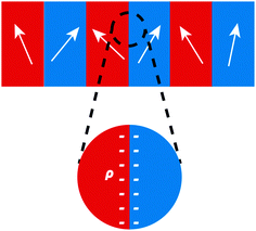
Ferroelectric materials are characterized by domains that are formed by the distribution of spontaneous polarization in space. A typical ferroelectric material with domains is shown in Fig. 1. The component of the polarization perpendicular to the domain boundary gives rise to bound charge at the boundary following26| ρpol = −∇·P | (1) |
3D drift-diffusion model
The structure of the planar perovskite solar cell used in the device simulation is as shown in Fig. 2. The crystalline structure of the perovskite is associated with well-defined valence and conduction bands separated by a band gap of 1.5 eV.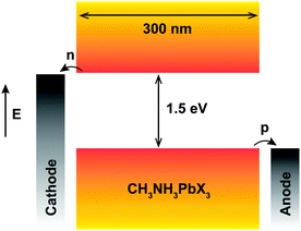 | ||
| Fig. 2 Device structure of the perovskite solar cell used in simulation. The energy offsets at both electrodes are 0.0 eV. | ||
In a typical planar perovskite solar cell with a p–i–n structure, the interface recombination at the doped hole (p) and electron (n) transport layer is found to be primarily dependent on the interface trap density and the energy level offsets,30–33 whereas the recombination in the perovskite absorber (i) layer is an intrinsic material property. Therefore, to exclusively study the charge recombination in the absorber layer, where the ferroelectric polarization is dominant, the p and n layers are not taken into account in the model. In addition, to disregard the role of any interface energy loss on the device performance, the valence band offset and the conduction band offset between anode/perovskite and perovskite/cathode, respectively, are set to 0.0 eV as seen in Fig. 2. Device structures without a transport layer were recently also studied experimentally, and shown to achieve high efficiencies including high open-circuit voltage.34–36
Our formulation of the 3D model is based on the drift-diffusion equations for electrons and holes throughout the device and on solving the Poisson's equation in three dimensions.37 In the perovskite layer, the absorption of light is shown to create both excitons and free charges.38,39 However, owing to the low exciton binding energy (22 meV),38 we assume the generation of free charges throughout the perovskite absorber. The transport of these free charges is then governed by diffusion and electrically induced drift; for electrons37
| Jn = −qnμn∇V + qDn∇n, | (2) |
| Jp = −qpμp∇V − qDp∇p. | (3) |
The electrostatic potential is solved from the Poisson's equation
 | (4) |
| q(VL − VR + Vapplied) = Wanode − Wcathode | (5) |
The electron (hole) density at the electrodes, in case of zero energy offset between the LUMO (HOMO) of the perovskite and the electrodes is given by the density of states, Nc/v, for the perovskite. Given the effective mass of charge carriers in the perovskite, m*, the density of states is calculated from the relation40
Nc/v = 2(2πm*kT/h2)![[/]](https://www.rsc.org/images/entities/char_e0ee.gif) | (6) |
Charge carriers in CH3NH3PbX3 can recombine via both, bimolecular and single carrier trapping (Shockley–Read–Hall) mechanism. However, being a direct band gap semiconductor,5,41 bimolecular recombination is found to be the dominant recombination process.42 In addition, experimental works have shown the density of traps to be low,43,44 suggesting minor impact on the solar cell performance. In our analysis, we model the charge recombination in the perovskite absorber in a bimolecular way, given by
| R = γnp | (7) |
 | (8) |
Device parameters
The parameter estimates for the device used in our simulation are shown in Table 1. Our calculations are based on a cell consisting of lead tri-halide perovskite (CH3NH3PbX3) as an absorber. The thickness of the perovskite absorber layer is assumed to be 300 nm which is typical for high performance perovskite solar cells.27 The generation of free charges, G = 5 × 1027 m−3 s−1 is assumed to be uniform throughout the absorber layer. Assuming the effective mass of carriers, m* ∼ 0.3 m0,46,47 the density of states of the valence and the conduction bands of the perovskite is calculated from eqn (6) to be Nc/v = 4.8 × 1024 m−3.| Parameter | Symbol | Value | Ref. |
|---|---|---|---|
| Perovskite thickness | L | 300 nm | 27 |
| Perovskite permittivity | ε | 6.5ε0 | 28 |
| Energy of conduction band in perovskite | Φ n | −3.9 eV | 29 |
| Energy of valence band in perovskite | Φ p | −5.4 eV | 29 |
| Hole mobility in perovskite | μ p | 2 cm2 V−1 s−1 | 6 |
| Electron mobility in perovskite | μ n | 2 cm2 V−1 s−1 | 6 |
The polarization in the perovskite is induced by the spontaneous feature i.e. the rotating methylammonium ions (MA) and the permanent PbX3 cage. Theoretical studies have estimated the value of the polarization density for the ferroelectric phase at room temperature to be a few μC cm−2.23,48 To examine the effect due to the permanent polarization on the photovoltaic working mechanism of perovksite solar cell, we initially perform calculations by considering a small polarization value of 0.05 μC cm−2 for the highly-ordered microstructures. For the realistic scenario of a microstructure with random correlated polarization, we then perform a study as a function of increasing value of polarization density.
We keep the pre-factor (γpre) equal to unity, which signifies high recombination strength, and then simulate the device with and without the presence of ferroelectric polarization in domains. In addition, we vary the size of domains from 15 nm to 100 nm. Finally, we simulate the device with low recombination strength (γpre = 10−4) as reported via experiments in the literature.10 A study as a function of the mobility and the langevin recombination pre-factor (γpre) is presented as additional simulation results in the ESI.†
Influence of ferroelectric polarization on device performance
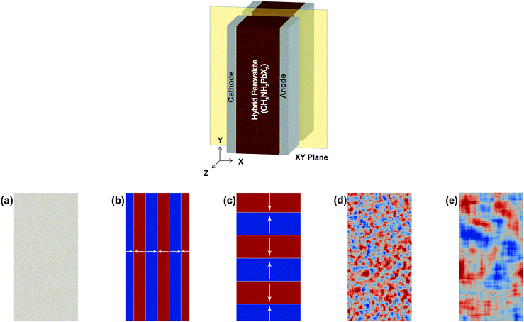
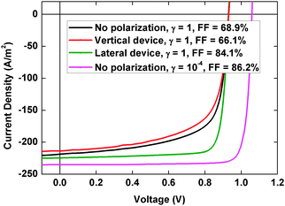
The various device microstructures considered in our calculations are shown in Fig. 3a–e. These structures differ in the polarization direction and in domain sizes. Fig. 3a shows the structure where no polarization exists in the perovskite (from here on, this structure is referred to as the reference structure). Fig. 3b and c show structures with polarization in the ±X and ±Y directions respectively (from here on, devices with these structures are referred to as vertical and lateral devices respectively). The approach used to obtain the short range (Fig. 3d) and long range (Fig. 3e) correlated structures is mentioned in the Methods section. Fig. 3d and e mimic the domain structures calculated by Frost et al. via the implementation of Monte-Carlo simulation of the polarized domain behavior in hybrid perovskites.24Given any structure, the bound charge is calculated on all domain boundaries (i.e. points where discontinuity in polarization occurs) following eqn (1) and is then incorporated in eqn (4) to be used in 3D drift diffusion simulation. For the high recombination strength (γpre = 1) scenario, the comparison between the simulated J–V characteristics of the perovskite solar cell for the model microstructures is shown in Fig. 4. As evidenced by the short-circuit current density (JSC) and fill factor (FF) values, the presence of ferroelectric polarization in domains significantly affects the macroscopic device performance. In all cases, the depolarizing electric field arising from the bound charges at domain boundaries results in accumulation of carriers at domain boundaries as seen from the carrier concentration profiles shown in Fig. 5. The domain boundaries are thus able to effectively separate the charge carriers in the bulk of the material. However, the mere presence of domain boundaries does not necessarily lead to efficient transport and extraction of carriers as explained below.
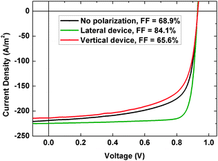 | ||
| Fig. 4 Simulated J–V curves for device with no polarization (Fig. 3a), vertical device (Fig. 3b) and lateral device (Fig. 3c). | ||
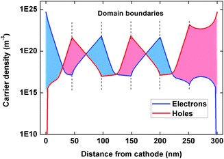 | ||
| Fig. 5 Carrier concentration profile at short-circuit conditions (Vapplied = 0 V) along the thickness of the vertical device structure as shown in Fig. 3b. The red and blue colored regions show the segregation of holes and electrons respectively, at the domain boundaries. | ||
The potential along the length of the device is mapped in Fig. 6 for the vertical and lateral structures. In the vertical device structure, the domain boundaries act as barriers for efficient carrier transport toward the electrodes. This results in extraction of fewer charge carriers (majority of which are between the electrodes and the first and the last domain boundary) at electrodes as compared to the device with no polarization, which leads to recombination at domain boundaries and an eventual loss in photocurrent. On the other hand, in the lateral device structure, charge carriers do not encounter any domain boundaries during their transport toward the extracting electrodes which explains the high photocurrent. The lateral domain boundaries can therefore be said to induce a channel-like behavior, where the segregated electrons and holes travel along the domain boundaries leading to efficient transport and low recombination loss. The fill factor (FF) which depends on the interplay between the charge transport, extraction and recombination in a device,49 is therefore the highest in the case of the lateral structure. Note that, even for small value of polarization density (0.05 μC cm−2), the lateral structure shows high FF (84.1%), very close to the calculated idealized limit for FF 88% for a solar cell with VOC = 0.93 V. For more information on the idealized limit for FF, please refer to the ESI.† A further increase in the polarization density would therefore only cause a marginal increase in FF as it approaches the idealized limit.
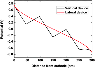 | ||
| Fig. 6 Potential landscape along the device thickness at short-circuit conditions (Vapplied = 0 V) for vertical and lateral structures. | ||
The vertical device structure has been recently studied in the context of inorganic ferroelectric photovoltaics, where the open-circuit voltage was shown to be higher than the band gap of the material.18,19 This phenomenon is a result of the high potential created by large number of domains boundaries with a potential step (ΔV > 10 mV) forming a thick device (few micrometers), in addition to the strong polarization of 30–40 μC cm−2 in some inorganic ferroelectrics including inorganic perovskites. Their negligible photocurrent18,19 can be explained by the strong polarization which produces massive depolarizing fields which forces majority of the charge carriers in the device to recombine. On the other hand, hybrid perovskites films used in PSCs are only a few hundred nanometers thick with fewer domain boundaries, and hybrid perovskites show a low polarization strength of only a few μC cm−2. This results in a weak depolarizing field arising from the bound charges on domain boundaries in hybrid perovskite films, which leads to only small potential step (ΔV) at domain boundaries and no significant alteration in the potential along the device. Therefore, no significant improvement in the open-circuit voltage is observed in the case of the vertical device structure in PSCs as seen in Fig. 4.
Fig. 7a and b show the simulated J–V curves for the lateral and vertical device respectively for variation in the size of domains. To examine the influence of domain size on the device performance of PSCs, we simulate the lateral and vertical device structures with domain sizes ranging from 15 to 100 nm under the consideration of high recombination strength. Large domains give rise to fewer domain boundaries in the device. In addition, the depolarizing field strength arising from the bound charges on domain boundaries falls inversely with squared distance, according to the Coulomb's law, from the domain boundaries into the domain bulk. This results in lower density of segregated charges at domain boundaries which can be efficiently extracted at the electrodes. Hence, devices with large domain size show poor performance as can be seen in Fig. 7a. In the case of lateral device structure, domain size smaller than 30 nm shows poor performance (not shown in figure). This is due to the recombination of segregated charges at adjacent domain boundaries, which increases with decrease in the domain size. For the case of vertical device structure, the photocurrent arises from the charge carriers segregated at domain boundaries close to the electrodes and the those charge carriers between the cathode and the first domain boundary, and between the anode and the last domain boundary. Since the decrease in the number of domain boundaries leads to fewer and thicker domains, the change in the photocurrent for the vertical device is not significant as seen from Fig. 7b. Now, if the polarization in the domains were to be strong, as is the case with some inorganic perovskites, the massive depolarizing field would result in recombination of majority of charge carriers at domain boundaries and the photocurrent would only originate from the charges between the electrodes and the first and last domain boundaries. This, once more echoes the observation of low photocurrent in inorganic perovskite devices. Also, as seen in Fig. 7b, the marginal increase in VOC with decrease in domain size or increase in number of domain boundaries agrees with the finding by Yang et al. where they observe increase in VOC with increase in the number of domain boundaries.18
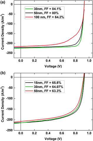 | ||
| Fig. 7 Simulated J–V curves for (a) lateral and (b) vertical device structures with different domain sizes. | ||
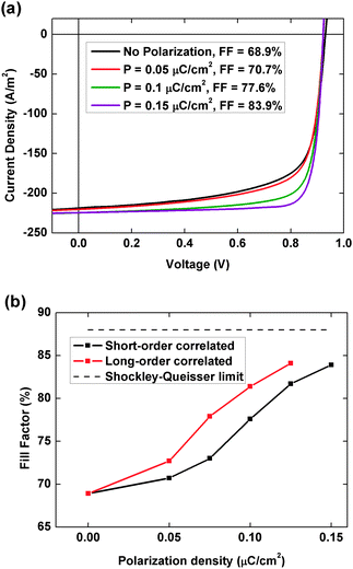
The highly ordered polarization domain microstructures shown in Fig. 3b and c are unlikely to occur in actual devices. In a systematic study, Frost et al. modeled the domain behavior by means of Monte-Carlo simulations providing insight into the formation of domain structures in hybrid perovskites.24 In order to study similar domain structures, we construct and simulate two complex structures with small (10 nm) and large (100 nm) domains defined by short-order and long-order correlated polarization in the perovskite as shown in Fig. 3d and e respectively. Fig. 8a compares the simulated J–V curves for different values of the polarization strength for short-order correlated microstructure. As can be seen, the fill factor (FF) is the parameter which is influenced most significantly with increasing polarization strength. The variation of the FF with polarization density is shown in Fig. 8b for both microstructures. As the FF is a directly influenced by the efficiency of charge transport and the degree of recombination in a solar cell, it is evident that the presence of polarization in the perovskite can result in enhanced charge transport and lowering of recombination in a perovskite solar cell (PSC). Since these complex microstructures can be considered to be a composite of the two previously discussed microstructures (Fig. 3b and c), the lateral structure (Fig. 3c) that shows high FF and channel like behavior for charge transport dominates the device operation in these complex microstructures. From Fig. 8b, the FF reaches 83.9% when P = 0.15 μC cm−2 for short-order correlated microstructure and 84.1% when P = 0.125 μC cm−2 for long-order correlated microstructure, which is very close to the idealized limit for FF 88% for a solar cell with VOC = 0.93 V. Although the ab initio value of polarization in the perovskite is reported to be few μC cm−2,23,48 an order of magnitude higher than considered here, a further increase in the value of polarization would lead to a marginal increase in FF.
In the case of vertical device (Fig. 3b), the increase in the polarization strength would lead to increase in the VOC and decrease in JSC and FF as shown in ref. 19. For the case of lateral device (Fig. 3c), increase in polarization strength would only result in a small increase in FF as the value approaches the idealized limit for FF.
We now consider the scenario of intrinsically low recombination strength in the perovskite by setting the pre-factor for bimolecular recombination, γpre = 10−4. This approximate value has been reported by Wehrenfenniget al. in their experimental work.10 The comparison between simulated J–V curves for the case with and without polarization in high recombination strength (γpre = 1) scenario, and no polarization in intrinsically low recombination strength (γpre = 10−4) scenario, is shown in Fig. 9. Depending on the microstructure, presence of polarization can either result in poor device performance as in the case of vertical domains or can give high fill factor and short-circuit current values as in the case of lateral domains and random correlated structures. However, no device structure is able to explain the high open-circuit voltage (1.1 V) which is characteristic of high performance PSCs.25,50 On the other hand, the device with intrinsically low recombination strength yields a FF of 86.2%, JSC of 235 A m−2 and notably, a high VOC of 1.08 V comparable to the VOC of high performance PSCs. This suggests that, the ferroelectric polarization is unlikely to explain the origin of high VOC of PSCs, and the origin is essentially intrinsic to the perovskite material.
Conclusions
We studied the influence of mesoscale ferroelectricity in perovskite film on the device performance of the perovskite solar cell, including the short-circuit current (JSC), the fill factor (FF), and the open-circuit voltage (VOC). We simulated the working of the solar cell with a 3D drift diffusion model and incorporated the mesoscale ferroelectricity in perovskite films by accounting for the bound charge on the polarized domain boundaries. To examine the role of ferroelectricity in the lowering of apparent charge recombination strength in the device, we considered two cases viz. (1) a high recombination strength (γpre = 1) in presence of ferroelectric polarization scenario, and (2) a low recombination strength (γpre = 10−4) scenario. In the context of charge recombination, we also investigated the effects that the orientation of the polarization in domains and the size of the domains has on the device performance of the solar cell. We showed that ferroelectric polarization in the perovskite material significantly influences the short-circuit current and fill factor of the solar cell.We demonstrated that the depolarizing field arising from bound charges is able to effectively separate opposite charge carriers in the bulk of the material resulting in the accumulation of charge carriers at domain boundaries. Polarization along the thickness of the device, which leads to formation of domains parallel to the electrodes, showed poor device performance as electrons and holes buildup at the domain boundaries and eventually recombine to give low short-circuit current and fill factor, with marginal improvement in open-circuit voltage. A device with ordered domains perpendicular to the electrodes and having polarization in the plane of the device showed high JSC and FF, as electrons and holes encounter no domain boundaries during their transport toward the electrodes. We also examined the influence of the domain size on the device performance, and showed that, for lateral devices the domain size significantly influences charge segregation and recombination dynamics in the device. For vertical devices, owing to the low polarization strength found in hybrid perovskites, the variation in domain size was found to have a marginal influence on the device characteristics.
The presence of highly-ordered polarized domains in the perovskite leads to creation of channels for efficient charge transport and lowering of charge recombination in the device which results into high fill factor (FF) and short-circuit current (JSC). Such ordering is however, unlikely to occur in actual devices. In the case of random correlated polarization in domains, a realistic scenario, we showed that electrons and holes appear to follow channels or pathways in the perovskite, giving rise to efficient charge transport and low charge recombination in the solar cell as evidenced by high FFs. Finally, we showed that the high VOC, which is distinctive feature of PSCs, can only be explained by the consideration of the intrinsically low recombination strength (γpre = 10−4) in hybrid perovskites.
Methods
Design of device microstructure with short-order and long-order correlated polarization
We fixed the average value of the polarization, Pavg in the perovskite to P = 0.05, 0.075, 0.1, 0.125, 0.15 μC cm−2. Initially, the polarization value and direction is set randomly for every grid point in 3D space. Now, a correlation is introduced by smoothing of polarization values at grid points enclosed in a averaging length (rx, ry and rz) in all three dimensions. The value of the averaging length determines the correlation range in the final structure. The structure shown in Fig. 3d was constructed by setting rx = ry = rz = 2 grid points, while the one shown in Fig. 3e was constructed by setting rx = ry = rz = 10 grid points. The smoothed correlated values were then renormalized with Pavg to obtain the final polarization map which defines the microstructures. We made ten realizations for each of the two microstructures.Acknowledgements
This is a publication by the FOM Focus Group ‘Next Generation Organic Photovoltaics’, participating in the Dutch Institute for Fundamental Energy Research (DIFFER). This work is part of the Industrial Partnership Programme (IPP) ‘Computational sciences for energy research’ of the Foundation for Fundamental Research on Matter (FOM), which is part of the Netherlands Organisation for Scientific Research (NWO). This research programme is co-financed by Shell Global Solutions International B.V.References
- G. Hodes, Science, 2013, 342, 317–318 CrossRef CAS PubMed.
- M. A. Green, A. Ho-Baillie and H. J. Snaith, Nat. Photonics, 2014, 8, 506–514 CrossRef CAS.
- N.-G. Park, Mater. Today, 2015, 18, 65–72 CrossRef CAS.
- H. J. Snaith, J. Phys. Chem. Lett., 2013, 4, 3623–3630 CrossRef CAS.
- A. Kojima, K. Teshima, Y. Shirai and T. Miyasaka, J. Am. Chem. Soc., 2009, 131, 6050–6051 CrossRef CAS PubMed.
- S. D. Stranks, G. E. Eperon, G. Grancini, C. Menelaou, M. J. Alcocer, T. Leijtens, L. M. Herz, A. Petrozza and H. J. Snaith, Science, 2013, 342, 341–344 CrossRef CAS PubMed.
- E. Edri, S. Kirmayer, S. Mukhopadhyay, K. Gartsman, G. Hodes and D. Cahen, Nat. Commun., 2014, 5, 3461 Search PubMed.
- N. J. Jeon, J. H. Noh, W. S. Yang, Y. C. Kim, S. Ryu, J. Seo and S. I. Seok, Nature, 2015, 517, 476–480 CrossRef CAS PubMed.
- W. S. Yang, J. H. Noh, N. J. Jeon, Y. C. Kim, S. Ryu, J. Seo and S. I. Seok, Science, 2015, 348, 1234–1237 CrossRef CAS PubMed.
- C. Wehrenfennig, G. E. Eperon, M. B. Johnston, H. J. Snaith and L. M. Herz, Adv. Mater., 2014, 26, 1584–1589 CrossRef CAS PubMed.
- J. M. Frost, K. T. Butler, F. Brivio, C. H. Hendon, M. Van Schilfgaarde and A. Walsh, Nano Lett., 2014, 14, 2584–2590 CrossRef CAS PubMed.
- S. Liu, F. Zheng, N. Z. Koocher, H. Takenaka, F. Wang and A. M. Rappe, J. Phys. Chem. Lett., 2015, 6, 693–699 CrossRef CAS PubMed.
- R. E. Cohen, Nature, 1992, 358, 136–138 CrossRef CAS.
- V. M. Fridkin and B. Popov, Sov. Phys. Usp., 1978, 21, 981 CrossRef.
- M. Qin, K. Yao and Y. C. Liang, Appl. Phys. Lett., 2008, 93, 122904 CrossRef.
- S. M. Young and A. M. Rappe, Phys. Rev. Lett., 2012, 109, 116601 CrossRef PubMed.
- T. Choi, S. Lee, Y. Choi, V. Kiryukhin and S.-W. Cheong, Science, 2009, 324, 63–66 CrossRef CAS PubMed.
- S. Yang, J. Seidel, S. Byrnes, P. Shafer, C.-H. Yang, M. Rossell, P. Yu, Y.-H. Chu, J. Scott and J. Ager, et al. , Nat. Nanotechnol., 2010, 5, 143–147 CrossRef CAS PubMed.
- J. Seidel, D. Fu, S.-Y. Yang, E. Alarcón-Lladó, J. Wu, R. Ramesh and J. W. Ager III, Phys. Rev. Lett., 2011, 107, 126805 CrossRef PubMed.
- H. Yi, T. Choi, S. Choi, Y. Oh and S.-W. Cheong, Adv. Mater., 2011, 23, 3403–3407 CrossRef CAS PubMed.
- Y. Kutes, L. Ye, Y. Zhou, S. Pang, B. D. Huey and N. P. Padture, J. Phys. Chem. Lett., 2014, 5, 3335–3339 CrossRef CAS PubMed.
- L. Bertoluzzi, R. S. Sanchez, L. Liu, J.-W. Lee, E. Mas-Marza, H. Han, N.-G. Park, I. Mora-Sero and J. Bisquert, Energy Environ. Sci., 2015, 8, 910–915 CAS.
- A. Stroppa, C. Quarti, F. De Angelis and S. Picozzi, J. Phys. Chem. Lett., 2015, 6, 2223–2231 CrossRef CAS PubMed.
- J. M. Frost, K. T. Butler and A. Walsh, APL Mater., 2014, 2, 081506 CrossRef.
- M. Grätzel, Nat. Mater., 2014, 13, 838–842 CrossRef PubMed.
- J. Guyonnet, Ferroelectric Domain Walls, Springer, Geneva, 2014 Search PubMed.
- C. Momblona, O. Malinkiewicz, C. Roldán-Carmona, A. Soriano, L. Gil-Escrig, E. Bandiello, M. Scheepers, E. Edri and H. Bolink, APL Mater., 2014, 2, 081504 CrossRef.
- M. Hirasawa, T. Ishihara, T. Goto, K. Uchida and N. Miura, Physica B, 1994, 201, 427–430 CrossRef CAS.
- P. Gao, M. Grätzel and M. K. Nazeeruddin, Energy Environ. Sci., 2014, 7, 2448–2463 CAS.
- H. Zhou, Q. Chen, G. Li, S. Luo, T.-B. Song, H.-S. Duan, Z. Hong, J. You, Y. Liu and Y. Yang, Science, 2014, 345, 542–546 CrossRef CAS PubMed.
- S. Ryu, J. H. Noh, N. J. Jeon, Y. C. Kim, W. S. Yang, J. Seo and S. I. Seok, Energy Environ. Sci., 2014, 7, 2614–2618 CAS.
- Q.-K. Wang, R.-B. Wang, P.-F. Shen, C. Li, Y.-Q. Li, L.-J. Liu, S. Duhm and J.-X. Tang, Adv. Mater. Interfaces, 2015, 2, 1400528 Search PubMed.
- D. Bi, L. Yang, G. Boschloo, A. Hagfeldt and E. M. Johansson, J. Phys. Chem. Lett., 2013, 4, 1532–1536 CrossRef CAS PubMed.
- S. Aharon, S. Gamliel, B. El Cohen and L. Etgar, Phys. Chem. Chem. Phys., 2014, 16, 10512–10518 RSC.
- A. Dymshits, A. Rotem and L. Etgar, J. Mater. Chem. A, 2014, 2, 20776–20781 CAS.
- S. Gamliel, A. Dymshits, S. Aharon, E. Terkieltaub and L. Etgar, J. Phys. Chem. C, 2015, 119, 19722–19728 CAS.
- D. Bartesaghi and L. J. A. Koster, Adv. Funct. Mater., 2015, 25, 2013–2023 CrossRef CAS.
- Q. Lin, A. Armin, R. C. R. Nagiri, P. L. Burn and P. Meredith, Nat. Photonics, 2014, 3, 106–112 CrossRef.
- A. Miyata, A. Mitioglu, P. Plochocka, O. Portugall, J. T.-W. Wang, S. D. Stranks, H. J. Snaith and R. J. Nicholas, Nat. Phys., 2015, 11, 582–587 CrossRef CAS.
- N. Ashcroft and N. Mermin, Solid State Physics, Saunders College, Philadelphia, 1976 Search PubMed.
- T. Baikie, Y. Fang, J. M. Kadro, M. Schreyer, F. Wei, S. G. Mhaisalkar, M. Graetzel and T. J. White, J. Mater. Chem. A, 2013, 1, 5628–5641 CAS.
- Y. Yamada, T. Nakamura, M. Endo, A. Wakamiya and Y. Kanemitsu, J. Am. Chem. Soc., 2014, 136, 11610–11613 CrossRef CAS PubMed.
- A. Baumann, S. Väth, P. Rieder, M. C. Heiber, K. Tvingstedt and V. Dyakonov, J. Phys. Chem. Lett., 2015, 6, 2350–2354 CrossRef CAS PubMed.
- D. Shi, V. Adinolfi, R. Comin, M. Yuan, E. Alarousu, A. Buin, Y. Chen, S. Hoogland, A. Rothenberger and K. Katsiev, et al. , Science, 2015, 347, 519–522 CrossRef CAS PubMed.
- L. J. A. Koster, O. Stenzel, S. D. Oosterhout, M. M. Wienk, V. Schmidt and R. A. Janssen, Adv. Energy Mater., 2013, 3, 615–621 CrossRef CAS.
- G. Giorgi, J.-I. Fujisawa, H. Segawa and K. Yamashita, J. Phys. Chem. Lett., 2013, 4, 4213–4216 CrossRef CAS PubMed.
- W.-J. Yin, J.-H. Yang, J. Kang, Y. Yan and S.-H. Wei, J. Mater. Chem. A, 2015, 3, 8926–8942 CAS.
- Y. Zhou, F. Huang, Y.-B. Cheng and A. Gray-Weale, Phys. Chem. Chem. Phys., 2015, 17, 22604–22615 RSC.
- D. Bartesaghi, I. del Carmen Pérez, J. Kniepert, S. Roland, M. Turbiez, D. Neher and L. J. A. Koster, Nat. Commun., 2015, 6, 7083 CrossRef CAS PubMed.
- H. S. Jung and N.-G. Park, Small, 2015, 11, 10–25 CrossRef CAS PubMed.
Footnote |
| † Electronic supplementary information (ESI) available: Additional simulation results. See DOI: 10.1039/c5cp07117h |
| This journal is © the Owner Societies 2016 |

