
 Open Access Article
 This Open Access Article is licensed under a
 Creative Commons Attribution 3.0 Unported Licence
Effects of Bi and Sb ion incorporation on the optoelectronic properties of mixed lead–tin perovskites†
F. M.
Rombach
 a,
L.
Gregori
bh,
A.
Sidler
c,
J.
Whitworth
d,
S.
Zeiske
ef,
H.
Jin
a,
E. Y.-H.
Hung
a,
S.
Motti
g,
P.
Caprioglio
a,
A.
Armin
e,
M.
Lenz
cj,
D.
Meggiolaro
*h,
F.
De Angelis
bhi and
H. J.
Snaith
*a
a,
L.
Gregori
bh,
A.
Sidler
c,
J.
Whitworth
d,
S.
Zeiske
ef,
H.
Jin
a,
E. Y.-H.
Hung
a,
S.
Motti
g,
P.
Caprioglio
a,
A.
Armin
e,
M.
Lenz
cj,
D.
Meggiolaro
*h,
F.
De Angelis
bhi and
H. J.
Snaith
*a
aDepartment of Physics, University of Oxford, Clarendon Laboratory, Parks Road, Oxford, OX1 3PU, UK. E-mail: henry.snaith@physics.ox.ac.uk
bDepartment of Chemistry, Biology and Biotechnology, University of Perugia and INSTM, Via Elce di Sotto 8, 06123, Perugia, Italy
cInstitute for Ecopreneurship, School of Life Sciences, University of Applied Sciences and Arts Northwestern Switzerland, Hofackerstrasse 30, 4132 Muttenz, Switzerland
dMaterials Innovation Factory, University of Liverpool, 51 Oxford Street, Liverpool L7 3NY, UK
eSustainable Advanced Materials (Sêr-SAM), Centre for Integrative Semiconductor Materials and Department of Physics, Swansea University Bay Campus, Fabian Way, Swansea, SA1 8EN, UK
fDepartment of Chemistry, Northwestern University, Evanston, IL 60208, USA
gSchool of Physics and Astronomy, Faculty of Engineering and Physical Sciences, University of Southampton, University Road, Southampton SO17 1BJ, UK
hComputational Laboratory for Hybrid/Organic Photovoltaics (CLHYO), Istituto CNR di Scienze e Tecnologie Chimiche “Giulio Natta” (CNR-SCITEC), Via Elce di Sotto 8, Perugia, 06123, Italy. E-mail: daniele.meggiolaro@cnr.it
iSKKU Institute of Energy Science and Technology (SIEST), Sungkyunkwan University, Suwon, 440-746, Korea
jDepartment of Environmental Technology, Wageningen University, Wageningen 6708 WG, the Netherlands
First published on 27th January 2025
Abstract
Doping with small densities of foreign ions is an essential strategy for tuning the optoelectronic properties of semiconductors, but the effects of doping are not well-understood in halide perovskites. We investigate the effect of Bi3+ and Sb3+ doping in lead–tin perovskites. Films doped with small amounts of BiI3 and SbI3 show greatly increased non-radiative recombination at precursor doping concentrations as low as 1 ppm for Bi3+ and 1000 ppm for Sb3+. We rationalize such behaviour by density functional theory (DFT) simulations, showing that these metal ions can be incorporated in the perovskite crystal by introducing deep trap levels in the band gap. Having found that very small amounts of Bi3+ greatly reduce the optoelectronic quality of lead–tin perovskite films, we investigate the presence of Bi impurities in perovskite precursor chemicals and find quantities approaching 1 ppm in some. In response, we introduce a facile method for removing Bi3+ impurities and demonstrate removal of 100 ppm Bi from a perovskite ink. This work demonstrates how the incorporation of small concentrations of foreign metal ions can severely affect film quality, raising the importance of precursor chemical purity.
1. Introduction
Lead halide perovskites (LHP) are outstanding materials for photovoltaics due to their excellent optoelectronic properties, such as direct band gaps, high absorption coefficients and long charge carrier lifetimes and diffusion lengths.1 The partial replacement of lead with tin narrows the band gap of the perovskite from 1.6 to ∼1.2 eV for lead–tin ratios around 40/60.2,3 Mixed lead–tin perovskites are thus promising materials for the development of single-junction as well as all-perovskite tandem solar cells in combination with neat LHPs.4Compared to LHPs, however, mixed lead–tin perovskites experience increased self-p-doping that may hinder their efficiencies in solar cells. When the amount of tin is comparable to lead, background hole densities in the range 1014–1017 cm−3 are reported.5–7 Such a wide range of reported values can be explained by variations in processing conditions between labs, particularly the extent of oxygen exposure before and during film deposition, which can strongly affect the density of Sn2+ vacancies. The increase in p-doping when moving from a lead-dominant to a tin-dominant perovskite composition is mainly due to a shift in the energy of the perovskite valence band maximum (VBM) towards the vacuum level, inducing a stabilization of the acceptor defects in the material. In parallel, the facile oxidation of tin(II) to tin(IV) promotes the formation of tin vacancies, limiting the long-term stability of the material.8,9
The ability to control the long-term stability and the self-p-doping level is of central importance for the full exploitation of lead–tin perovskites in solar cells. Reducing the background hole density below 1015 cm−3 is expected to improve energetic alignment,10 as well as reduce loss pathways involving the recombination of photo-excited electrons with the hole background.11 The use of SnF2 and Sn metal additives has been shown to successfully limit tin oxidation and the incorporation of Sn4+ during the perovskite film deposition.7,12,13 However, the magnitude by which these strategies can reduce self-p-doping in Sn-based perovskites is limited.12
Shifting the Fermi level of halide perovskites has been found to be surprisingly challenging compared to other semiconductor materials.14 Whilst both intrinsic doping (by under- or over-stoichiometric precursor ratios) and extrinsic doping (by the introduction of lattice impurities) have been successfully used to somewhat increase background carrier densities, large shifts in Fermi level remain elusive. Theoretical investigation suggests that this is mainly due to the facile formation of compensatory intrinsic defects in perovskite in response to doping, and the difficulty in finding dopants with formation energies of their presence in the lattice much smaller than the most stable structural defect.15
One strategy to control the p-doping and possibly increase the stability of lead–tin perovskites while retaining the native band gap is doping with metal ions. The incorporation of these ions may move the Fermi level in these materials by both directly introducing free carriers by ionization or by affecting the formation energies of intrinsic defects, inducing a shift in defect chemistry. Previously, heterovalent metal dopants such as Rb+, K+, Na+, Ga3+ and Ag+ have been demonstrated to increase the formation energies of Sn vacancies and passivate I− vacancies or iodine trimers, reducing non-radiative recombination rates in a range of perovskite compositions.16–21 There have also been previous experimental indications that the background carrier density of perovskites may be modulated through doping, e.g. by Ga3+ in lead–tin perovskites,18 and Bi3+ in neat lead perovskites.22 A challenge associated with doping is that metal ions much smaller or larger than Sn2+/Pb2+ are unlikely to be incorporated in the lattice at significant densities,22,23 be incorporated preferentially at interfaces,18 or even migrate out of the perovskite structure over time, reversing the effects of doping.17 In addition to this, the charge imbalance introduced by the incorporation of heterovalent dopants is expected to be partially compensated by the formation of negatively charged defects such as Pb2+ vacancies, A-cation vacancies or I− interstitials,18,22 which will not only decrease doping efficiency but may also negatively impact optoelectronic properties. Hence, the impact of metal dopants on the Fermi level of halide perovskites depends not only upon their ionization energy, but also on their effect on the formation energies of native perovskite defects.
Due to the comparable ionic radius and the similar electronic structure, Bi and Sb metals appear as a natural choice for n-doping, and hence compensate the self-p-doping and increasing the lattice stability of lead–tin perovskites. They are suggested to n-dope by incorporating in the perovskite in their 3+ charge state.24,25 Previous experimental works, however, have highlighted the emergence of deep trap states associated with the Bi3+ dopant in neat lead perovskites, strongly impacting the optoelectronic properties by increased non-radiative recombination.26–29 Such observations are in agreement with theoretical predictions.24,25 Recent computational studies on neat-Sn perovskite compositions found both Bi and Sb introduce deep recombination levels even when lead was entirely substituted by Sn.30 The deep ionization levels associated with the dopants shift down in energy by moving from lead to tin perovskite, keeping their deep nature. This is mainly due to the increase in energy of the VBM of the perovskite moving from lead to tin. A recent investigation on the effects of relatively large concentrations of Bi doping (1+%) of mixed lead–tin perovskites found that Bi also induces increased non-radiative recombination in these materials. Although Sb3+ doping has also been indicated to slightly n-dope neat lead perovskites, it has not been as widely explored.31,32 The effects of small densities of both Bi3+ and Sb3+ doping on lead–tin perovskites hence remain unexplored.
In this work we investigate the impact of Bi3+ and Sb3+ metal dopants on the optoelectronic properties of mixed lead–tin perovskites. We explore a wide range of dopant concentrations down to 0.01 ppm and find that Bi3+ doping densities as low as 1 ppm (corresponding to a Bi3+ density of ∼1015 cm−3 in the film) severely quench the photoluminescence of the perovskite. Sb3+ doping is also found to quench photoluminescence, but only at significantly higher densities of 100 ppm. The observed increase in non-radiative recombination is rationalized using DFT simulations. These show that both Bi3+ and Sb3+ can incorporate into the lattice of lead–tin perovskites, but induce deep electron traps in the band gap, similarly to what has been previously observed in neat lead perovskites. The disastrous impact of very small amounts of Bi3+ on the optoelectronic quality of the perovskite poses serious concerns regarding its presence as a potential impurity in perovskite precursor chemicals. Motivated by this, we carried out chemical impurity analysis of different precursor powders and found that in some precursors Bi is present in amounts that could affect perovskite quality. In response, we develop and validate a strategy to remove Bi3+ impurities from perovskite precursor chemicals based on reduction by Sn0 metal.
2. Results & discussion
2.1 Optoelectronic quality of Bi3+ and Sb3+-doped lead–tin perovskite films
To investigate the effects of Bi3+ and Sb3+ doping on the optoelectronic properties of mixed lead–tin perovskites, we fabricated perovskite films with 0.001 ppm (10−7% in the precursor solution, or 1 × 1012 cm−3 in the films) to 50![[thin space (1/6-em)]](https://www.rsc.org/images/entities/char_2009.gif) 000 ppm (5%, or 5 × 1019 cm−3) dopant. Films were doped by adding BiI3 and SbI3 (from stock solutions) to the filtered perovskite precursor solution, after which the precursor was stirred for 60 minutes. As SbI3 was found to be less soluble in these solvents, it could only be investigated up to a doping density of 1000 ppm (0.1%, or 1 × 1018 cm−3). The higher concentrations of Bi3+ and Sb3+ caused a clear reddish discoloration of the perovskite precursor solution. Bi3+ and Sb3+ are expected to be incorporated into the perovskite lattice at the metal cation position (Fig. 1a). Although the dopant added to the precursor solution may not entirely incorporate in the perovskite bulk at the higher concentrations, we expect that the density of incorporated dopant will follow the trend of dopant precursor concentration. For example, for Bi doping of MAPbBr3 it has been shown that Bi is incorporated into the lattice at approximately the same concentration as BiBr3 in the perovskite precursor solution.28 Throughout our paper, references to dopant density refer to the concentration of dopant added to the perovskite precursor solution, with respect to the sum of the lead and tin concentrations.
000 ppm (5%, or 5 × 1019 cm−3) dopant. Films were doped by adding BiI3 and SbI3 (from stock solutions) to the filtered perovskite precursor solution, after which the precursor was stirred for 60 minutes. As SbI3 was found to be less soluble in these solvents, it could only be investigated up to a doping density of 1000 ppm (0.1%, or 1 × 1018 cm−3). The higher concentrations of Bi3+ and Sb3+ caused a clear reddish discoloration of the perovskite precursor solution. Bi3+ and Sb3+ are expected to be incorporated into the perovskite lattice at the metal cation position (Fig. 1a). Although the dopant added to the precursor solution may not entirely incorporate in the perovskite bulk at the higher concentrations, we expect that the density of incorporated dopant will follow the trend of dopant precursor concentration. For example, for Bi doping of MAPbBr3 it has been shown that Bi is incorporated into the lattice at approximately the same concentration as BiBr3 in the perovskite precursor solution.28 Throughout our paper, references to dopant density refer to the concentration of dopant added to the perovskite precursor solution, with respect to the sum of the lead and tin concentrations.
 | ||
| Fig. 1 (a) Schematic illustrating trivalent doping of hybrid lead–tin perovskites. Bi3+ or Sb3+ incorporate at the substitutional Pb2+ site. The partial charge compensation by the formation of Sn2+/Pb2+ vacancies is also illustrated. (b) PLQE of lead–tin perovskite films doped with small quantities of (i) Bi3+ or (ii) Sb3+. (c) Absorbance around the band edge of lead–tin perovskite films doped with various amounts of Bi3+ and Sb3+. (d) Ultra-sensitive EQE measurements of electrically contacted lead–tin perovskite films doped with various amounts of Bi3+. | ||
Perovskite thin films were successfully deposited by solution processing from precursors containing the Bi3+ and Sb3+ doping densities described, with no significant visible differences in film drying and curing. We characterized these films by X-ray diffraction (XRD) (Fig. S1, ESI†) and found that the original lead–tin perovskite phase is unchanged for all concentrations of Bi3+ and Sb3+ tested. Optical measurements of both Bi3+ and Sb3+-doped films confirm this by showing no shift in band gap for the full range of doping densities. We did observe a slight reduction in XRD scattering peak intensity at Bi3+ densities above 5000 ppm. When 50000 ppm Bi3+ was added, we also observed two new XRD peaks corresponding to BiI3, suggesting that at this precursor concentration there is a significant amount of excess Bi3+ which is not incorporated in the perovskite crystal. This is consistent with previous studies on single crystals of Bi doped MAPbBr3, where Bi incorporation could be observed up to around 50000 ppm doping.27,28
To map the effect of Bi3+ and Sb3+ doping on the optoelectronic quality of the lead–tin perovskite films, we performed steady-state photoluminescence quantum efficiency (PLQE) measurements. Samples were excited with a red 660 nm laser at an intensity which resulted in an absorbed photon flux equivalent to AM 1.5 1 sun conditions for a 1.25 eV bandgap material. Surprisingly, we found that very small amounts of Bi3+ doping led to a severe decrease in the PLQE of the lead–tin perovskite films (Fig. 1b(i)), with the addition of 1 ppm Bi3+ causing an ∼80% reduction in PLQE with respect to undoped samples. To confirm, we also performed time-resolved photoluminescence (TRPL) decay measurements on the same samples and fitted the tails of the decays with a mono-exponential decay (Fig. S2, ESI†). The dynamics show an identical trend to the PLQE, with 1 ppm Bi3+ causing a ∼10-fold decrease in lifetime with respect to controls. This suggests that the addition of even very small densities of Bi3+ severely increases the rate of non-radiative recombination in PbSn perovskites. This is consistent with previous observations of Bi3+ doping in neat lead perovskites, in which 10 ppm Bi3+ was observed to already reduce device performance.26
Doping the lead–tin perovskite in the same manner with Sb3+ revealed that this dopant similarly increases non-radiative recombination rates in the perovskite films, but at significantly higher concentrations of 100–1000 ppm (Fig. 1b(ii)). For doping densities that did not completely quench the photoluminescence (below 1 ppm for Bi3+ and 1000 ppm for Sb3+), we found no change in either the position or the shape of the PL emission peak (Fig. S3, ESI†). Whilst previous investigations of Bi3+ doping in MAPbBr3 observed an enhanced emission in the region of 1000–1080 nm in the doped films,27–29 we did not observe any new emission peaks at longer wavelengths up to our detector limit of 1400 nm.
We could not discern significant changes to the above bandgap absorption properties, as measured by UV-vis-NIR transmission and reflectance spectrophotometry (Fig. 1c). To probe more subtle changes that may occur in the sub-bandgap region of the absorption onset and tail, we performed ultra-sensitive external quantum efficiency (EQE) measurements on electrically contacted Bi3+-doped lead–tin perovskite films.33 Films doped with 10000 ppm Bi3+ show a significant broadening of the EQE onset (Fig. 1d). This can be ascribed to increased energetic disorder, which has previously also been observed by others in Bi3+-doped neat Pb perovskites.26–29 However, for films doped with 10 ppm Bi3+, both EQE and absorptance spectra were found to be very similar to films without any Bi3+, despite the PLQE being strongly quenched at this density. Analogously, we also observed no change in the absorptance spectra of Sb3+-doped films up to 1000 ppm density. Hence, we conclude that at impurity levels between 1–10 ppm for Bi3+ and above 100 ppm for Sb3+, doping with these elements does not affect electronic disorder to an observable extent but does significantly increase the rate of non-radiative recombination. This would be consistent with the Bi3+ and Sb3+ dopants creating highly recombination-active traps in the perovskite, which cause rapid recombination even at densities that do not observably increase electronic disorder.
2.2 DFT simulations
To rationalize the observed impact of Bi3+ and Sb3+ on the lead–tin perovskite, we investigated the efficacy of their incorporation and their effect on the electronic band structure and defect energies of MAPb0.5Sn0.5I3 through DFT calculations. For simplicity, we have chosen MA as the mono-valent cation for the DFT calculations. Since the band structure near the CB minimum and VB maxima are dominated by the divalent metal and halide orbitals, and the crystal structure and lattice constant of a formamidinium/cesium mixed cation perovskite is similar to the MA perovskite, we do not expect that the choice of monovalent cation will significantly influence the calculated defect energies induced by the group V metal doping. Dopant equilibrium structures were obtained by using the Perdew–Burke–Ernzherof (PBE) functional34 in the 2 × 2 × 2 supercell of the phase with densities of ∼3%, see Computational details in ESI.†As expected, DFT analysis highlights that the incorporation of the dopants is thermodynamically more favorable in substitutional position to Pb and Sn than other positions in the lattice, e.g. interstitial or substitutional to the organic cation (see Table S1 of ESI†). Furthermore, the incorporation in substitutional position to Pb is slightly more favorable than on the Sn site for both Bi and Sb (see Table S1 and Fig. S4, ESI†), due to the more similar ionic radius of the dopants with lead. Hence, our defect analysis has been focused on dopants in substitutional position to Pb in the lattice. To provide accurate defect properties, the defect formation energies and thermodynamic ionization levels (TIL) have been calculated by using the PBE0 hybrid functional (α = 0.20)35,36 and by including spin–orbit coupling (SOC), see Computational details.
In Fig. 2a the calculated defect formation energies of the substitutional dopants in I-medium conditions of growth are reported and compared to defect formation energies of the most stable native defects in MAPb0.5Sn0.5I3, i.e. V2−Pb, V2−Sn, I−i and V+I. Bi dopant is stable in the positive state of charge (+III oxidation state) for Fermi levels up to 0.52 eV, where a deep (+/0) transition is present and the neutral state becomes the stable form of the defect. In heavily n-doped perovskites (Fermi level close to the conduction band) the negative form of the defect is also stable. Due to the similar ionic radius of Bi3+ (103 pm) and Pb2+ (119 pm), Bi3+ incorporation in the Pb site leads to a limited metal–iodide bond variation with respect to the pristine perovskite (see Fig. 3a). The analysis of the projected density of states (PDOS) of Bi+Pb shows that the dopant introduces a localized Kohn–Sham (KS) level in the band gap of the perovskite placed at ∼1.0 eV above the VBM (see Fig. 3b). Such a state traps one electron upon photoexcitation leading to an occupied KS level placed at 0.3 eV above the VBM, after lattice relaxation (Fig. 3b). Upon the relaxation, an elongation of the Bi–I bond lengths is observed due to the population of the antibonding state of the metal.
 | ||
| Fig. 2 (a) Defect formation energies of substitutional BiPb and SbPb dopants compared with the more stable native defects in MAPb0.5Sn0.5I3 (I-medium conditions); (b) associated thermodynamic ionization levels. Defect quantities have been calculated at PBE0-SOC (α = 0.20) level of theory by including DFT-D3 dispersions. | ||
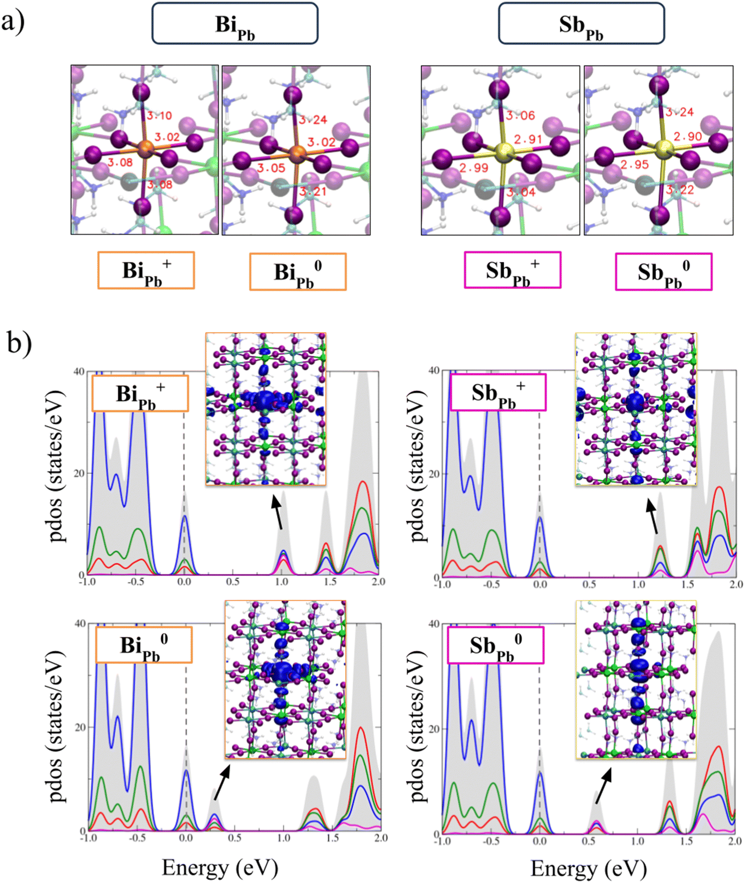 | ||
| Fig. 3 (a) Equilibrium structures of the positive and neutral BiPb, SbPb defects; (b) atom-projected density of states (PDOS) of the same defects, highlighting the presence of deep trap states in the band gap of the perovskite (blue = I, red = Pb, green = Sn, purple = dopant). In the diagrams the VBM energy is set to zero (dotted line). In the insets the plots of the LUMO (HOMO) Kohn–Sham (KS) orbitals of the positive (neutral) defects are reported. | ||
The in-gap nature of the LUMO state suggests that no barriers to the trapping of the electron on the Bi+Pb defect are present. We have investigated the non-radiative recombination of the hole on the neutral Bi0Pb defect by calculating the energy-coordinate diagram of the neutral and positive defect along distortion of the Bi–I bond, see Fig. S7 of ESI.† We have highlighted in the diagram, the presence of a small barrier (0.18 eV) to the recombination of the hole. This indicates that the inclusion of Bi strongly increases electron trapping and subsequent non-radiative recombination in the material.
Compared to Bi, Sb is stable in the +III oxidation state in a wider Fermi level range, with the positive charged state being the most stable form of the defect up to 0.92 eV above the VBM, i.e. the position of the (+/0) deep transition, see Fig. 2. Similarly to Bi, Sb is preferentially incorporated in the +III oxidation state in thermodynamic equilibrium, i.e. Sb+Pb. Due to the smaller radius, Sb3+ introduces a slight contraction of the metal–iodide bonds, see Fig. 3. The analysis of the electronic structure of the Sb+Pb defect highlights the presence of an unoccupied orbital below the CBM that after the electron trapping leads to the formation of an occupied KS level placed at ∼0.6 eV above the VBM, as reported in the PDOS of the neutral charged state (Fig. 3). The (+/0) ionization level of Sb occurs at higher energy with respect to Bi, i.e. 0.9 eV vs. 0.5 eV above the VBM, highlighting that Sb is a less active charge trap compared to Bi. Notably, the different behavior is attributed to the more limited SOC effects on the p-orbitals of the Sb with respect to Bi, since without inclusion of relativistic effects the energy difference between the (+/0) transitions in the two cases is around 0.1 eV, see Fig. S4 of ESI.†
In principle, the defect equilibrium obtained after the incorporation of the dopants could have an impact on the charge carrier equilibrium density. In the pristine perovskite the native Fermi level is placed at around 0.3 eV above the VBM and it is mainly set by the equilibrium between iodine vacancies and lead vacancies. After the incorporation of Bi and Sb the DFT calculations predict that the Fermi level shifts by 0.2 eV towards the middle of the band gap, with a decrease in hole density of around four orders of magnitude. If there were no other consequences of the Bi or Sb doping, this significant Fermi level shift would be advantageous.
If completely incorporated in the perovskite structure, the addition of 1 ppm Bi3+ would lead to a trap state density of 1015 cm−3 (substituting 0.0001% of the 1021 cm−3 Pb/Sn sites in the perovskite lattice). To investigate whether such a density of deep defects can completely explain the observed increase in non-radiative recombination, we performed TRPL and PLQE simulations which are presented in Fig. 5. We find that when modelling Bi as a mid-gap trap (0.625 eV from CB) with symmetrical hole and electron capture coefficients of 10−8 cm−3 s−1, a density of 1015 cm−3 (equivalent to the full incorporation of 1 ppm Bi) can indeed closely replicate the reductions in PLQE and TRPL lifetimes observed in the films, with only a slight deviation in the early-time shape of the TRPL decay.
However, performing the same simulation with a shallower trap (0.35 eV from the CB) to simulate the effect of Sb doping shows that the shallower energy level of Sb in the perovskite lattice cannot completely explain the reduced impact on non-radiative recombination (Fig. 4b). We find that the TRPL and PLQE results can be well-reproduced when assuming that only 0.3% of the added Sb incorporates in the perovskite lattice. Alternatively, the electron and hole capture coefficients of the Sb defect may in reality be lower than estimated here. Based on DFT predictions, no remarkable differences in the incorporation energies of Bi and Sb have been observed. Hence, the less severe effect of Sb3+ doping on non-radiative recombination rates and energetic disorder may be explained by a combination of a shallower trap energy and a kinetic hindrance to the incorporation of Sb3+ ions which are more strongly solvated with respect to Bi3+ in the precursor solution.
 | ||
| Fig. 4 Simulated TRPL decays and PLQE values with varying trap types and densities. TRPL and PLQE variation with (a) Bi trap density variation (0.625 eV from CB, equal hole and electron capture coefficients of 10−8 cm3 s−1), (b) Sb trap density variation (0.3 eV from CB, equal hole and electron capture coefficients of 10−8 cm3 s−1), and (c) shallow hole trap such as V2−Pb/Sn or I−i variation (0.15 eV from CB, asymmetrical hole and electron capture coefficients of 10−8, 10−10 cm3 s−1 respectively) (i) without additional Bi traps and (ii) with 1015 cm−3 additional Bi traps. All additional simulation parameters are given in the methods. | ||
Defect formation energy analysis confirms that the incorporation of Bi and Sb is largely compensated by the formation of lead or tin vacancies V2−Pb/Sn, while the formation of compensating iodine interstitials I−i shows more unfavorable thermodynamics, see Table 1. Previous computational studies on neat-lead perovskites demonstrated that non-radiative recombination on the Bi+Pb defect is hindered by the presence of a thermodynamic barrier to recombination. The loss of performance of Bi-doped perovskite solar cells was instead attributed to Fermi level shift induced by the dopant, increasing the density of deep acceptor defects, i.e. iodine interstitials, in the material.37 Whilst we expect Bi doping to cause a similarly large increase in the V2+Pb/Sn and I−i acceptor defects here, both of these defects were previously calculated to be relatively shallow defects in the bulk of mixed lead–tin perovskites, with a distance from the VB not exceeding 0.15 eV.8 We hence presume that their recombination activity is limited. To test the effect of an increase in the density of these shallow defects, we simulated their effect on PLQE and TRPL decays (Fig. 4c). We found that indeed, an increase in shallow defect density could not by itself recreate the severe decrease in PLQE and TRPL lifetime we observed without showing a very strong trap-filling feature in the first 10 ns of the TRPL decay (not observed in our experimental data). However, increasing the shallow defect density in addition to a 1015 cm−3 Bi trap density produced simulations that match the experimental TRPL decay shape better (Fig. 4c(i)). Hence, our simulations suggest that compensatory shallow defects contribute to recombination processes, but Bi/Sb defects determine overall non-radiative recombination rates. This evidence, together with the small barrier to recombination predicted by incorporation of the dopants is thermodynamically more favorable, suggest that the increased non-radiative recombination in of Bi- and Sb-doped films is mainly due to the direct trapping-recombination on the dopant sites. Encouragingly, this indicates that n-doping Sn-containing perovskites is not always doomed to increase non-radiative recombination, as the compensatory acceptor defects formed seem only minimally recombination-active.
| Reaction | M = Bi (eV) | M = Sb (eV) |
|---|---|---|
| (R1) 3/2PbPb + MI3 → M+Pb + 1/2V2−Pb + 3/2PbI2 | 0.12 | 0.14 |
| (R2) PbPb + MI3 → M+Pb + I−i + PbI2 | 0.50 | 0.53 |
2.3 Bi3+ impurities in perovskite precursor chemicals
The deleterious effect of very small amounts of Bi3+ doping (1 ppm) on the optoelectronic properties of lead–tin perovskites raises concerns about the potential presence of Bi3+ as an impurity in perovskite precursor chemicals. Even very high purity precursors normally only quote purity to 15 ppm and could thus have impurities on this scale (0.0001%). We tested a range of lead–tin perovskite precursor powders for Bi and Sb impurities by ICP-MS and were able to detect these elements to a sensitivity of 0.01 ppm. The type, supplier, and purity of each precursor we investigated is listed in Table S2 (ESI†), and the absolute Bi and Sb impurity densities determined by ICP-MS are presented in Table 2. These are representative of impurity concentrations that can be present under the typical operating conditions of a metal halide perovskite-producing laboratory, under which cross-contamination cannot be fully excluded. Even with strict fabrication procedures and cleanliness protocols, contamination may occur while precursor chemicals are stored in a glovebox area where Bi and Sb are also stored and occasionally handled. In addition, we emphasize that at such low impurity concentrations, batch-to-batch variation is likely and hence this data is not necessarily representative of other batches of a certain material or supplier.| Contaminant concentration (ppm) | ||
|---|---|---|
| Sb (mean ± stdev) | Bi (mean ± stdev) | |
| a Signifies a minimum amount, as some solids remained after sample digestion which were deemed insoluble in nitric acid. | ||
| FAI | 0.580 ± 0.225 | 0.057 ± 0.059 |
| CsI | 0.356 ± 0.057 | 0.027 ± 0.017 |
| PbI2 | 0.025 ± 0.002 | 0.026 ± 0.005 |
| SnI2 (A) | 0.204a ± 0.008 | Not detected (<0.01) |
| SnI2 (B) | 0.298a ± 0.002 | 1.059a ± 0.012 |
| SnF2 | 1.816a ± 0.047 | 1.613a ± 0.065 |
| Sn(0) | 0.476a ± 0.010 | 0.198a ± 0.002 |
The concentration of Bi which each precursor chemical would deliver to the perovskite ink (a 1.8 M dispersion of FA0.83Cs0.17Pb0.5Sn0.5I3 with 10% SnF2 and 10 mg ml−1 Sn0) is shown in Fig. 5a. In our case, no precursors contributed significant levels of Sb (>10 ppm), but one precursor contributed possibly significant levels of Bi (>0.1 ppm) to the solution. This was the SnI2 precursor labelled ‘B’, at 0.5 ppm. However, when we fabricated perovskite films made using this SnI2 and compared them to films made using an alternate SnI2 precursor containing no detected Bi (labelled ‘A’), we found no significant difference in PLQE (Fig. S7, ESI†). One possible explanation for this is that the Bi impurity could be present in its metallic neutral state within the precursor, since ICP-MS cannot determine in which oxidation state a trace impurity exists. Sn is more readily oxidized than Bi, so it is feasible that Bi impurities remain in their neutral state during the synthesis of SnI2. Bi0 is not expected to become dissolved in the perovskite ink, as neither Pb2+ nor Sn2+ are expected to be able to oxidize it, and as such the presence of Bi0 impurities in perovskite precursor chemicals is not expected to lead to Bi3+ doping of the perovskite.
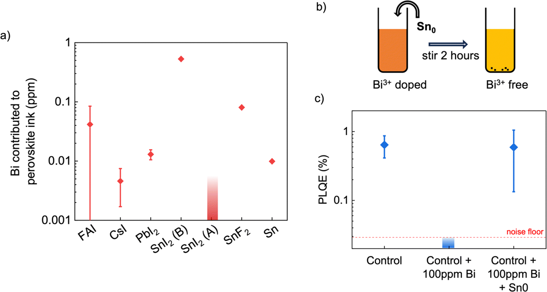 | ||
| Fig. 5 (a) Bi density, in ppm with respect to combined Pb and Sn content, contributed to FA0.83Cs0.17Pb0.5Sn0.5I3 perovskite precursor ink by commercial precursor chemicals, as determined by ICP-MS. (b) Schematic illustrating treatment of Bi3+-containing perovskite precursor ink with Sn0 powder to reduce and remove Bi3+. (c) PLQE of lead–tin perovskite films without any Bi3+ doping, doped with 100 ppm Bi3+, and doped with 100 ppm Bi3+ and subsequently treated with Sn0 for 1 hour, showing complete recovery of PLQE after Sn0 treatment. | ||
Although not demonstrated to be significant in our case, Bi3+ impurities could certainly present a problem for the field of perovskite photovoltaics in general, particularly when large quantities of precursors are needed for scaling up. We propose a facile solution for removing Bi3+ impurities by treating the perovskite ink with a small amount of Sn0 metal powder before filtering. Both Sn and Pb are more readily oxidized than Bi, which means that the following reaction is expected to take place between Sn0 and Bi3+ (eqn (1)).
| 3Sn0(s) + 2Bi3+(sol) ⇒ 2Bi0(s) + 3Sn2+(sol) | (1) |
3. Conclusion
In conclusion, we investigated the effect of Bi3+ and Sb3+ doping in lead–tin halide perovskite and demonstrated that both dopants strongly increase the rate of non-radiative recombination within the perovskite. Through DFT simulations, we have shown that Bi3+ and Sb3+ can be stably incorporated in the perovskite lattice in the substitutional position to Pb2+, where they directly induce deep electron trap states within the band gap of the material. Ultimately, we conclude that the strong charge trapping activity of Bi3+ and Sb3+ makes them unsuitable for use as n-dopants in tin-based perovskites.Our experiments showed that while lead–tin perovskites are more tolerant towards the presence of Sb3+ in the perovskite precursor, they are extremely sensitive to the incorporation of Bi3+, showing quenched photoluminescence at concentrations as low as 1 ppm. We found that some precursors contribute bismuth concentrations approaching 0.5 ppm to the perovskite precursor ink but reveal that the use of these precursors did not result in films with significantly accelerated non-radiative recombination, possibly due to Bi impurities existing in their metallic rather than ionic form. However, these Bi3+ impurities can be easily removed from perovskite precursors by stirring with metallic Sn0 powder. Using this method, we demonstrate the successful removal of 100 ppm Bi from our perovskite precursor such that the electronic quality of the resulting film is equal to that of undoped films.
This work demonstrates how very small impurity concentrations can strongly affect films quality and hence highlights the importance of precursor chemical purity. It also raises the need to screen potential perovskite dopants for the creation of potential trap states that lie within the perovskite bandgap, which may vary not only by dopant but also by perovskite composition.
Data availability
Data for this article are available at Oxford Research Archives at https://dx.doi.org/10.5287/ora-kqdreg40y.Conflicts of interest
H. J. S. is co-founder and chief scientific officer of Oxford PV Ltd, a company commercializing perovskite PV technology.Acknowledgements
This project received funding from the engineering and physical sciences research council (EPSRC), UK, under grant EP/S004947/1, the Royal Society International Exchange program, under grant IEC\R2\202294. Funded by the European Union. Views and opinions expressed are however those of the author(s) only and do not necessarily reflect those of the European Union or RIA or CINEA. Neither the European Union nor the granting authority can be held responsible for them. VALHALLA project has received funding from Horizon Europe Research and Innovation Action programme under Grant Agreement n° 101082176. M. L. and A. S. acknowledge funding from the Swiss State Secretariat for Education, Research and lnnovation (SERI) (within the European Union NEXUS project). A. A. and S. Z. acknowledge the funding and support by the UKRI through the EPSRC Program Grant EP/T028513/1 Application Targeted and Integrated Photovoltaics. This work made use of shared equipment located at the Materials Innovation Factory; created as part of the UK Research Partnership Innovation Fund (Research England) and co-funded by the Sir Henry Royce Institute. H. J. acknowledges the support of the sponsorships from Oxford PV. E. Y. H. thanks Xaar for PhD scholarship sponsorship.References
- M. A. Green, A. Ho-Baillie and H. J. Snaith, The Emergence of Perovskite Solar Cells, Nat. Photonics, 2014, 8(7), 506–514, DOI:10.1038/nphoton.2014.134.
- M. T. Klug, R. L. Milot, J. B. Patel, T. Green, H. C. Sansom, M. D. Farrar, A. J. Ramadan, S. Martani, Z. Wang, B. Wenger, J. M. Ball, L. Langshaw, A. Petrozza, M. B. Johnston, L. M. Herz and H. J. Snaith, Metal Composition Influences Optoelectronic Quality in Mixed-Metal Lead–Tin Triiodide Perovskite Solar Absorbers, Energy Environ. Sci., 2020, 13(6), 1776–1787, 10.1039/D0EE00132E.
- K. J. Savill, A. M. Ulatowski and L. M. Herz, Optoelectronic Properties of Tin–Lead Halide Perovskites, ACS Energy Lett., 2021, 6(7), 2413–2426, DOI:10.1021/acsenergylett.1c00776.
- M. T. Hörantner, T. Leijtens, M. E. Ziffer, G. E. Eperon, M. G. Christoforo, M. D. McGehee and H. J. Snaith, The Potential of Multijunction Perovskite Solar Cells, ACS Energy Lett., 2017, 2(10), 2506–2513, DOI:10.1021/acsenergylett.7b00647.
- C. C. Stoumpos, C. D. Malliakas and M. G. Kanatzidis, Semiconducting Tin and Lead Iodide Perovskites with Organic Cations: Phase Transitions, High Mobilities, and Near-Infrared Photoluminescent Properties, Inorg. Chem., 2013, 52(15), 9019–9038, DOI:10.1021/ic401215x.
- J. Thiesbrummel, V. M. Le Corre, F. Peña-Camargo, L. Perdigón-Toro, F. Lang, F. Yang, M. Grischek, E. Gutierrez-Partida, J. Warby, M. D. Farrar, S. Mahesh, P. Caprioglio, S. Albrecht, D. Neher, H. J. Snaith and M. Stolterfoht, Universal Current Losses in Perovskite Solar Cells Due to Mobile Ions, Adv. Energy Mater., 2021, 2101447, DOI:10.1002/aenm.202101447.
- K. J. Savill, A. M. Ulatowski, M. D. Farrar, M. B. Johnston, H. J. Snaith and L. M. Herz, Impact of Tin Fluoride Additive on the Properties of Mixed Tin–Lead Iodide Perovskite Semiconductors, Adv. Funct. Mater., 2020, 30(52), 2005594, DOI:10.1002/adfm.202005594.
- D. Meggiolaro, D. Ricciarelli, A. A. Alasmari, F. A. S. Alasmary and F. De Angelis, Tin versus Lead Redox Chemistry Modulates Charge Trapping and Self-Doping in Tin/Lead Iodide Perovskites, J. Phys. Chem. Lett., 2020, 11(9), 3546–3556, DOI:10.1021/acs.jpclett.0c00725.
- D. Ricciarelli, D. Meggiolaro, F. Ambrosio and F. De Angelis, Instability of Tin Iodide Perovskites: Bulk p-Doping versus Surface Tin Oxidation, ACS Energy Lett., 2020, 5(9), 2787–2795, DOI:10.1021/acsenergylett.0c01174.
- F. Pena-Camargo, J. Thiesbrummel, H. Hempel, A. Musiienko, V. M. L. Corre, J. Diekmann, J. Warby, T. Unold, F. Lang, D. Neher and M. Stolterfoht, Revealing the Doping Density in Perovskite Solar Cells and Its Impact on Device Performance, Appl. Phys. Rev., 2022, 9, 021409 CAS.
- R. L. Milot, G. E. Eperon, T. Green, H. J. Snaith, M. B. Johnston and L. M. Herz, Radiative Monomolecular Recombination Boosts Amplified Spontaneous Emission in HC(NH2)2SnI3 Perovskite Films, J. Phys. Chem. Lett., 2016, 7(20), 4178–4184, DOI:10.1021/acs.jpclett.6b02030.
- R. L. Milot, M. T. Klug, C. L. Davies, Z. Wang, H. Kraus, H. J. Snaith, M. B. Johnston and L. M. Herz, The Effects of Doping Density and Temperature on the Optoelectronic Properties of Formamidinium Tin Triiodide Thin Films, Adv. Mater., 2018, 30(44), 1804506, DOI:10.1002/adma.201804506.
- R. Lin, K. Xiao, Z. Qin, Q. Han, C. Zhang, M. Wei, M. I. Saidaminov, Y. Gao, J. Xu, M. Xiao, A. Li, J. Zhu, E. H. Sargent and H. Tan, Monolithic All-Perovskite Tandem Solar Cells with 24.8% Efficiency Exploiting Comproportionation to Suppress Sn(II) Oxidation in Precursor Ink, Nat. Energy, 2019, 4(10), 864–873, DOI:10.1038/s41560-019-0466-3.
- J. Euvrard, Y. Yan and D. B. Mitzi, Electrical Doping in Halide Perovskites, Nat. Rev. Mater., 2021, 6(6), 531–549, DOI:10.1038/s41578-021-00286-z.
- F. P. Sabino, A. Zunger and G. M. Dalpian, Intrinsic Doping Limitations in Inorganic Lead Halide Perovskites, Mater. Horiz., 2022, 9(2), 791–803, 10.1039/D1MH01371H.
- R. Shi and R. Long, Atomic Model for Alkali Metal-Doped Tin–Lead Mixed Perovskites: Insight from Quantum Dynamics, J. Phys. Chem. Lett., 2023, 14(11), 2878–2885, DOI:10.1021/acs.jpclett.3c00602.
- F. Liu, J. Jiang, Y. Zhang, C. Ding, T. Toyoda, S. Hayase, R. Wang, S. Tao and Q. Shen, Near-Infrared Emission from Tin–Lead (Sn–Pb) Alloyed Perovskite Quantum Dots by Sodium Doping, Angew. Chem., Int. Ed., 2020, 59(22), 8421–8424, DOI:10.1002/anie.201916020.
- Z. Chang, D. Zheng, S. Zhao, L. Wang, S. Wu, L. Liu, Z. Li, L. Zhang, Q. Dong, H. Wang, S. Wang, K. Wang and S. (Frank) Liu, Designing Heterovalent Substitution with Antioxidant Attribute for High-Performance Sn–Pb Alloyed Perovskite Solar Cells, Adv. Funct. Mater., 2023, 33(22), 2214983, DOI:10.1002/adfm.202214983.
- C. Park, J. Choi, J. Min and K. Cho, Suppression of Oxidative Degradation of Tin–Lead Hybrid Organometal Halide Perovskite Solar Cells by Ag Doping, ACS Energy Lett., 2020, 5(10), 3285–3294, DOI:10.1021/acsenergylett.0c01648.
- S. R. Sahamir, M. A. Kamarudin, T. S. Ripolles, A. K. Baranwal, G. Kapil, Q. Shen, H. Segawa, J. Bisquert and S. Hayase, Enhancing the Electronic Properties and Stability of High-Efficiency Tin–Lead Mixed Halide Perovskite Solar Cells via Doping Engineering, J. Phys. Chem. Lett., 2022, 13(13), 3130–3137, DOI:10.1021/acs.jpclett.2c00699.
- B. Chen, Z. Yu, A. Onno, Z. Yu, S. Chen, J. Wang, Z. C. Holman and J. Huang, Bifacial All-Perovskite Tandem Solar Cells, Sci. Adv., 2022, 8(47), eadd0377, DOI:10.1126/sciadv.add0377.
- A. L. Abdelhady, M. I. Saidaminov, B. Murali, V. Adinolfi, O. Voznyy, K. Katsiev, E. Alarousu, R. Comin, I. Dursun, L. Sinatra, E. H. Sargent, O. F. Mohammed and O. M. Bakr, Heterovalent Dopant Incorporation for Bandgap and Type Engineering of Perovskite Crystals, J. Phys. Chem. Lett., 2016, 7(2), 295–301, DOI:10.1021/acs.jpclett.5b02681.
- K. Kobayashi, H. Hasegawa, Y. Takahashi, J. Harada and T. Inabe, Electronic Properties of Tin Iodide Hybrid Perovskites: Effect of Indium Doping, Mater. Chem. Front., 2018, 2(7), 1291–1295, 10.1039/C7QM00587C.
- E. Mosconi, B. Merabet, D. Meggiolaro, A. Zaoui and F. De Angelis, First-Principles Modeling of Bismuth Doping in the MAPbI3 Perovskite, J. Phys. Chem. C, 2018, 122(25), 14107–14112, DOI:10.1021/acs.jpcc.8b01307.
- J. L. Lyons, Effective Donor Dopants for Lead Halide Perovskites, Chem. Mater., 2021, 33(15), 6200–6205, DOI:10.1021/acs.chemmater.1c01898.
- M. Yavari, F. Ebadi, S. Meloni, Z. S. Wang, T. C.-J. Yang, S. Sun, H. Schwartz, Z. Wang, B. Niesen, J. Durantini, P. Rieder, K. Tvingstedt, T. Buonassisi, W. C. H. Choy, A. Filippetti, T. Dittrich, S. Olthof, J.-P. Correa-Baena and W. Tress, How Far Does the Defect Tolerance of Lead-Halide Perovskites Range? The Example of Bi Impurities Introducing Efficient Recombination Centers, J. Mater. Chem. A, 2019, 7(41), 23838–23853, 10.1039/C9TA01744E.
- A. M. Ulatowski, A. D. Wright, B. Wenger, L. R. V. Buizza, S. G. Motti, H. J. Eggimann, K. J. Savill, J. Borchert, H. J. Snaith, M. B. Johnston and L. M. Herz, Charge-Carrier Trapping Dynamics in Bismuth-Doped Thin Films of MAPbBr 3 Perovskite. J. Phys, Chem. Lett., 2020, 11(9), 3681–3688, DOI:10.1021/acs.jpclett.0c01048.
- P. K. Nayak, M. Sendner, B. Wenger, Z. Wang, K. Sharma, A. J. Ramadan, R. Lovrinčić, A. Pucci, P. K. Madhu and H. J. Snaith, Impact of Bi3+ Heterovalent Doping in Organic–Inorganic Metal Halide Perovskite Crystals, J. Am. Chem. Soc., 2018, 140(2), 574–577, DOI:10.1021/jacs.7b11125.
- R. Meng, G. Wu, J. Zhou, H. Zhou, H. Fang, M. A. Loi and Y. Zhang, Understanding the Impact of Bismuth Heterovalent Doping on the Structural and Photophysical Properties of CH3NH3PbBr3 Halide Perovskite Crystals with Near-IR Photoluminescence, Chem. – Eur. J., 2019, 25(21), 5480–5488, DOI:10.1002/chem.201805370.
- L. Gregori, D. Meggiolaro and F. De Angelis, Combining Trivalent Ion-Doping with Halide Alloying to Increase the Efficiency of Tin Perovskites, Small, 2024, 2403413, DOI:10.1002/smll.202403413.
- L. Huang, S. Bu, D. Zhang, R. Peng, Q. Wei, Z. Ge and J. Zhang, Schottky/P-n Cascade Heterojunction Constructed by Intentional n-Type Doping Perovskite Toward Efficient Electron Layer-Free Perovskite Solar Cells, Sol. RRL, 2019, 3(2), 1800274, DOI:10.1002/solr.201800274.
- J. R. Palmer, J. Yang, A. Gupta, C. J. Dolan, B. W. Larson, S. P. Dunfield, A. Mannodi-Kanakkithodi and D. P. Fenning, Bismuth in Lead–Tin Alloy Perovskites: Effect on Material Properties and Photovoltaic Device Performance, ACS Appl. Energy Mater., 2024, 7(7), 2726–2734, DOI:10.1021/acsaem.3c03156.
- S. Zeiske, C. Kaiser, P. Meredith and A. Armin, Sensitivity of Sub-Bandgap External Quantum Efficiency Measurements of Solar Cells under Electrical and Light Bias, ACS Photonics, 2020, 7(1), 256–264, DOI:10.1021/acsphotonics.9b01531.
- J. P. Perdew, K. Burke and M. Ernzerhof, Generalized Gradient Approximation Made Simple, Phys. Rev. Lett., 1996, 77(18), 3865–3868, DOI:10.1103/PhysRevLett.77.3865.
- J. P. Perdew, M. Ernzerhof and K. Burke, Rationale for Mixing Exact Exchange with Density Functional Approximations, J. Chem. Phys., 1996, 105(22), 9982–9985, DOI:10.1063/1.472933.
- C. Adamo and V. Barone, Toward Reliable Density Functional Methods without Adjustable Parameters: The PBE0 Model, J. Chem. Phys., 1999, 110(13), 6158–6170, DOI:10.1063/1.478522.
- X. Zhang, J.-X. Shen, M. E. Turiansky and C. G. Van De Walle, Hidden Role of Bi Incorporation in Nonradiative Recombination in Methylammonium Lead Iodide, J. Mater. Chem. A, 2020, 8(26), 12964–12967, 10.1039/D0TA04968A.
- T. Nakamura, S. Yakumaru, M. A. Truong, K. Kim, J. Liu, S. Hu, K. Otsuka, R. Hashimoto, R. Murdey, T. Sasamori, H. D. Kim, H. Ohkita, T. Handa, Y. Kanemitsu and A. Wakamiya, Sn(IV)-Free Tin Perovskite Films Realized by in Situ Sn(0) Nanoparticle Treatment of the Precursor Solution, Nat. Commun., 2020, 11(1), 3008, DOI:10.1038/s41467-020-16726-3.
Footnote |
| † Electronic supplementary information (ESI) available. See DOI: https://doi.org/10.1039/d4tc02162b |
| This journal is © The Royal Society of Chemistry 2025 |