
 Open Access Article
 This Open Access Article is licensed under a
 Creative Commons Attribution 3.0 Unported Licence
Ultra-high absorption efficiency of InN nanowires with a wide bandwidth in the short-wave infrared range†
Yanmeng Chua,
ZhouXiang Chena,
Hanchen Zhua,
Linjun Zhanga,
Fuxiang Shang a,
Qichao Houa,
Lulu Chena,
Wenzhang Fangab,
Yishu Zhangab,
Zhiyuan Cheng*a and
Yunyan Zhang
*ab
a,
Qichao Houa,
Lulu Chena,
Wenzhang Fangab,
Yishu Zhangab,
Zhiyuan Cheng*a and
Yunyan Zhang
*ab
aCollege of Integrated Circuits, Zhejiang University, Hangzhou, Zhejiang 311200, China. E-mail: zycheng@zju.edu.cn; yunyanzhang@zju.edu.cn
bZhejiang Technology Innovation Center of CMOS IC Manufacturing Process and Design, Hangzhou 311200, China
First published on 3rd March 2025
Abstract
The group III–V semiconductor InN is a highly promising candidate for photoelectric detectors in the short-wave infrared (SWIR) range but faces significant challenges in material quality. In recent years, one-dimensional nanowires (NWs) have allowed their high-quality growth and have added structural advantages. However, the performance potential of InN NWs is little known. Here, the optoelectrical properties of hexagonal wurtzite InN NWs were systematically studied. The high absorptivity of InN itself, along with the antenna effect and leaky model resonance, results in the InN NWs exhibiting more than 99% light absorption in the 1000–1470 nm range and a wide range of incidence angles (0–65°). The absorption of InN NW arrays with a low filling factor (FF) of 12.83% can be 34% higher than that of thin film materials of the same thickness and an additional 28% enhancement can be obtained by tilting the NWs. A remarkable response of up to 1 A W−1 can be explicitly achieved at 1550 nm with precisely arranged InN nanowire arrays. This responsivity is 11.83% higher than that of InGaAs nanowire arrays. The results indicate that InN NWs with outstanding light absorption performance can be used as an efficient photosensitive material in the SWIR range for photovoltaics, detectors, and other optoelectronic devices.
 Yunyan Zhang | Yunyan Zhang received his Ph.D. degree from the Department of Electronic & Electrical Engineering at University College London in 2015. He is currently a professor at Zhejiang University. His current research interests include the integration of III–V and GeSn semiconductor devices for advanced microelectronics and optoelectronics. He has published >80 papers, with >30 papers in Tier 1 level journals with an impact factor ≥10, such as Nano Today, ACS Nano, Small, and Nano Letters. |
Introduction
Indium nitride (InN) is a thermodynamically stable group III–V wurtzite compound that exhibits a narrow direct and nearly invariant band gap with temperature.1,2 Currently, the bandgap of InN has been proven to be close to 0.7 eV, enabling its absorption cutoff edge to precisely cover the two most crucial communication bands in the short-wave infrared (SWIR) spectrum: 1310 nm and 1550 nm. More importantly, the absorption coefficient of InN surpasses those of indium gallium arsenide (InGaAs) and germanium (Ge), ubiquitous materials employed in SWIR photoelectric applications. The analysis presented in Fig. 1 provides a comparative evaluation of the light absorption characteristics of bulk InN against InGaAs3 and Ge.4 Notably, the graph illustrates that InN exhibits a 1.8 times higher absorption coefficient than InGaAs at 1550 nm. This remarkable difference underscores the profound potential of InN in advancing the fields of optics and optoelectronics in applications requiring enhanced SWIR sensitivity. In addition, InN possesses the highest electron mobility (up to 12![[thin space (1/6-em)]](https://www.rsc.org/images/entities/char_2009.gif) 000 cm2 V−1·s at 300 K (ref. 5)) within group III-nitride semiconductors. Due to the advantages of nitride materials, InN can potentially achieve a high-temperature application compared with other materials. Additionally, InN demonstrates a maximum saturation velocity of 6 × 107 cm s−16 and a minimum effective electron mass of 0.07m0.5 These attributes, which facilitate efficient carrier transport, position InN as a highly attractive contender for a wide range of applications, including terahertz field devices,7 ultrafast optical switchers,8 high-frequency electronic devices,9 etc. Consequently, InN emerges as a promising candidate for developing next-generation optical devices.
000 cm2 V−1·s at 300 K (ref. 5)) within group III-nitride semiconductors. Due to the advantages of nitride materials, InN can potentially achieve a high-temperature application compared with other materials. Additionally, InN demonstrates a maximum saturation velocity of 6 × 107 cm s−16 and a minimum effective electron mass of 0.07m0.5 These attributes, which facilitate efficient carrier transport, position InN as a highly attractive contender for a wide range of applications, including terahertz field devices,7 ultrafast optical switchers,8 high-frequency electronic devices,9 etc. Consequently, InN emerges as a promising candidate for developing next-generation optical devices.
 | ||
| Fig. 1 Comparison of the absorption coefficients of InN, InGaAs,3 and Ge4 with the responsivity performance of detectors with the same device structure in the SWIR range. | ||
The challenge of producing high-quality InN was primarily due to the difficulty in epitaxially growing single crystals on suitable or appropriate substrates, resulting in a prolonged misconception regarding its band gap, which was erroneously believed to be approximately 2 eV.10–12 Nevertheless, the realization of a higher-quality InN film grown through molecular beam epitaxy (MBE) or metal–organic chemical vapor deposition (MOCVD), along with theoretical calculations, has revealed that its actual band gap is approximately 0.7 eV.13,14 Furthermore, the exceptional characteristics of InN, including pronounced light absorption15 and minimal inter-valley scattering,16 render it highly suitable for achieving ultra-fast response and high efficiency in the detection of SWIR wavelength ranges, particularly at the communication band of 1310/1550 nm. Ultrafast and highly efficient optoelectronic conversion modules are crucial in various domains, including deep-space communication,17 last-mile access,18 temporary link establishment, areas with vulnerable radio-frequency signal devices,19 and densely populated metropolitan areas.20
The production of high-quality InN films is presently constrained to the process of epitaxial growth, which is mainly carried out on sapphire substrates21 or gallium nitride (GaN) templates22 with 25.40% and 21.27% lattice mismatch, respectively. The epitaxy of InN films on silicon (Si) substrates directly is accompanied by a significant lattice mismatch of up to 35.24%,23 resulting in the formation of a considerable quantity of defects, thus leading to a degradation in the device performance.24 This limitation poses challenges in integrating InN devices with complementary metal–oxide–semiconductor (CMOS) technology and the scalability of the production.
One-dimensional nanowires (NWs) can alleviate the constraints through radial elastic strain relaxation, offering a cost-effective solution for high-quality integration on Si substrates.25,26 Meanwhile, utilizing NWs as light-absorption materials for detectors also offers notable benefits. NWs have been found to exhibit enhanced light absorption per unit volume by significantly increasing light trapping compared to planar film-based devices with a much smaller amount of materials.27 Thus, the utilization of NWs holds considerable importance in the context of small-scale detectors. Substantial investigation has been carried out on single NW28 and periodic NW arrays29 to find the optimum structural characteristics suitable for photodetection applications. NW arrays can support a broader range of optical absorption modes, encompassing localized30 models, leaky model resonance, Fabry–Perot modes, and whispering-gallery modes,31 which can enhance and achieve a broad wavelength range of light absorption. In addition, a series of comprehensive electromagnetic simulations are conducted to investigate the diverse morphology-dependent absorption properties of NWs with various cross-sections, including square, circular, hexagonal, and triangular configurations.32,33 The obtained spectra of various cross-sections exhibit qualitative similarities, such as similar absorption peaks and analogous absorption enhanced mode, but slight variations in absorption intensity. These findings indicate the excitation of similar optical resonances across all structural configurations.33 In the case of group III–V materials, indium phosphide (InP) NW arrays with a height of 2 μm have shown a remarkable ability to absorb over 90% of incident energy from both transverse electric- (TE, where the electric field is perpendicular to the axis) and transverse magnetic (TM, where the electric field aligns parallel to the axis)-polarised light, even at incidence angles of up to 60° (ref. 34 and 35) in the visible light band. However, the absorption properties under varying structural parameters of group III–V NW arrays and the mechanism of light absorption in the SWIR range have not been elucidated yet.
In this paper, we conduct comprehensive research on the optical absorption characteristics of single and arrays of hexagonal wurtzite InN NWs. The enhanced mode including the antenna effect, the focus effect, leaky model resonance, etc. elucidates the dependence of the absorption enhancement mechanism on the NW size, height, tilt angle, and spacing over a broad wavelength spectrum. This deep understanding of their optical properties is a crucial foundation for designing next generation, high-performance NW photoelectric detection devices.
Results and discussion
Absorption mode analysis
All the calculation analyses were performed using the finite element method in COMSOL to reveal critical structural features determining the optical properties of hexagonal InN NWs. Fig. 2(a) provides a cross-sectional illustration that schematically depicts the configuration of a single InN NW, where “D” denotes the internal dimension of the regular hexagonal NW. The single NW is surrounded by air, with a perfectly matched layer (PML) enclosing the air to capture scattered light. Additionally, a scattering boundary condition (SBC) is applied to the outer surface of the PML. It is assumed that the NW extends infinitely in the axial direction. The utilization of this reduced 2D model has proven to be a valuable method for promptly determining the absorption mode and the light absorption characteristics of NWs.32,36 The incident light is directed perpendicular to the NW's axis, as indicated by the rainbow arrows above the NW. This assumption is practical since light absorption primarily occurs along the axial direction. The refractive index of InN is reported by F. Bechstedt et al.,37 while the real part of the refractive index for air was set as 1 and the imaginary part was set as 0. | ||
| Fig. 2 (a) Schematic of the 2D cross-section of a single hexagonal InN NW. (b) Absorption coefficient of the hexagonal InN NW as a function of wavelength (λ) and diameter (D). | ||
The absorption efficiency of unpolarized light is denoted as Qabs, which demonstrates a significant increase of more than one across a broad spectrum of wavelengths in the case of individual NW configurations, as seen in Fig. 2(b). This phenomenon means that a single NW possesses the capability to capture incoming photons beyond their physical cross-sectional area and thus is recognized as the “optical antenna effect”.36 The maximum absorption is observed at shorter near-ultraviolet wavelengths, where the absorption cross-section is nearly three times the physical cross-section, suggesting that InN has more significant potential for absorption at ultraviolet wavelengths. The increase in diameter results in an elevated absorption within the near-ultraviolet region. Besides, as the parameter diameter increases, two distinct peaks in Qabs experience a redshift, leading to plateaus that signify a notable enhancement in Qabs within the SWIR region. The intensity of the higher plateau gradually rises and reaches its local maximum at D = 320 nm where λ = 1245 nm, with Qabs reaching 132.5%, followed by a rapid decrease.
To establish the relationship between distinct enhanced absorption modes and the enhancement in the absorption of an NW, a subset of representative NW diameters that demonstrate one or more enhanced absorption peaks has been selected for further research, as indicated by grey dashed lines in Fig. 3(a) and (b). The enhancement peaks are designated as first, second, third, etc., in the ascending order of diameter. This analysis was achieved by examining the distribution of the electric field intensity |E| inside the NWs at the respective enhanced peaks, as illustrated in Fig. 3(c)–(h). The energy flow density and direction within the NWs, i.e., the Poynting vector, are also depicted. When photons impinge upon the NWs’ surface, their optical trajectories experience refraction due to the high refractive index of InN compared to air, leading to a bending of optical paths. This refraction causes the incident light to converge towards the lower central region of the NW, a phenomenon referred to as the “focus effect”, as illustrated by the directional energy flow arrows. Consequently, NWs exhibit an amplified nano-focusing effect and thus enhanced absorption strength. The first enhancement peak of TE arises from this focus effect, as shown in Fig. 3(c).
 | ||
| Fig. 3 Qabs of the single hexagonal InN NW as a function of λ and D under (a) TE- and (b) TM-polarized illumination. Distribution of the electric field intensity |E| inside the hexagonal InN NW for the corresponding peak indicated by grey dashed lines: (c)–(f) the 1st enhanced peak to the 4th enhanced peak under TE-polarized incidence; (g) and (h) the 1st enhanced peak to the 2nd enhanced peak under TM-polarized incidence. | ||
The second peak indicates that a larger diameter NW adopts different absorption enhancement mechanisms. The absorbed incident light becomes leaky and interacts with the outside medium, working as a valuable antenna. Many studies have proven that leaky mode resonance (LMR)38 can serve as the prominent contribution factor to augmentation of absorption for numerous nanostructures. When the incident wavelength coincides with one of the allowed LMRs, the incident light interacts with the re-emitted light, resulting in an amplified |E| intensity within the NWs. Consequently, the NW can efficiently capture and configure light inside its limits. Thus, light absorption and the subsequently generated photocurrent could be selectively increased at a desired wavelength by adjusting the NW diameters. TEml and TMml (where “m” and “l” represent the azimuthal mode number and radial order of the resonances, respectively) correspond to distinct LMR enhancement modes, as depicted in Fig. 3(c)–(h). The TE11 mode depicted in Fig. 3(d) contributes to the second highly enhanced Qabs in Fig. 3(a).
As the diameter of the NW continues to increase, the situation will continue to change. The third Qabs peak can be ascribed to the Fabry–Perot-type modes. When light is introduced into NWs, it will be scattered or reflected by the dielectric interface; consequently, the light will constructively interfere with itself, resulting in energy stored within the resonance cavity.
The fourth peak combines several higher-order modes (Fig. 3(f)). The hybrid mode plays a significant role in achieving the highest level of light absorption over the whole spectrum. Incident light with shorter wavelengths is prone to be absorbed at the surface, so the maximum absorption occurs due to the larger diameter.
Fig. 3(g) demonstrates that the first enhancement in absorption associated with the TM-polarized incidence arises from the resonance of the focus effect. Fig. S1† depicts a distribution diagram of the magnetic field intensity |H| that makes this phenomenon more apparent. The electric field intensity |E| is primarily concentrated at the radial periphery of the NW, whereas it becomes negligible in the core region. On the other hand, the field intensity associated with TM polarization is primarily localized inside the core region of the NW. This phenomenon is the reason behind the comparatively reduced absorption efficiency of TE polarization compared to TM polarization. It is notable that the second peak associated with the mixture of higher-order resonance modes, as shown in Fig. 3(h), contributes considerably to the overall Qabs in the short-wavelength region.
This phenomenon underscores the profound influence of NW diameter on regulating absorption modes within NWs. For photo-sensing applications such as photodetectors or photovoltaics, the current density can be optimized by tuning the diameters of NWs to better match the incident wavelength to obtain the maximum response. Consequently, the Qabs spectra exhibit a pronounced reliance on the individual NW parameters, matching with the distinctive resonance mode.
While the absorption mode of a single NW has been examined, the utilization of regularly arranged NW arrays in the device offers greater practicality for many applications such as photodetectors,39 solar cells,40 biosensors,41 metamaterials,42 light emitters43 and so on. The NW arrays exhibit distinct absorption characteristics compared to individual NWs as multiple reflections of light within NW arrays are influenced by complex dimensional parameters such as height, the aspect ratio between height and diameter, and spacing. It is imperative to investigate the impact of these parameters to fully exploit the potential of NW arrays.
Absorptance of 3D NW arrays
A periodic 3D NW array model is illustrated in Fig. 4(a). Assuming integration with CMOS technology, NW arrays are grown on a Si substrate. The NW diameter is still represented as “D”, while “P” signifies the period of the unit cell, and the height of the NW is represented as “H”. Here, D was set to 400 nm and P was set to 800 nm. Periodic boundary conditions are utilized to reduce computational complexity and improve processing efficiency. The periodic conditions are defined along the x and y axes with NWs surrounded by air. The upper boundary of the air and the lower boundary of the Si substrate are designated as PMLs to capture the scattered light. The incident light is perpendicular to the x–y plane. | ||
| Fig. 4 (a) The periodic model of the InN NW array. The absorption spectrum of NW arrays under (b) TE- and (c) TM-polarized incidence. (d)–(g) The longitudinal section of distribution of the electric field intensity |E| inside the 3D hexagonal InN NW under TE-polarized incidence with different NW heights and incident wavelengths. | ||
For the 3D NW absorption model, the absorptance A(λ) of NW arrays is given by A(λ) = 1 − R(λ) − T(λ), where R(λ) is the reflectance and T(λ) is transmittance. As depicted in Fig. S2,† the absorptance A(λ) dependence on the λ with diverse heights of the Si substrate is obtained under TE-polarized incidence. The Si substrate exhibits negligible absorption beyond 1000 nm and essentially no absorption after 1100 nm, corresponding to the Si absorption cut-off wavelength. Furthermore, it appears that the thickness of the substrate has minimal impact on the absorption characteristics of the NW arrays. In our subsequent models, the substrate thickness was set to 3 μm. Our primary focus lies on the absorptance of the NW arrays beyond 1000 nm.
The influence of NW height on the absorptance of the NW array was evaluated using the absorptance obtained under TE- and TM-polarized incidence. The absorption spectrum exhibits similarities for both TE- and TM-polarized incidences, as depicted in Fig. 4(b) and (c). As the NW height increases from 1 μm to 3.5 μm, the absorptance gradually rises while the absorptance reaches the maximum at 1436 nm. With a continuous increase in NW height, the absorptance of NW arrays reaches saturation over 95% absorptance across a wide range of wavelengths before the cut-off wavelength (∼1860 nm). Fig. 4(b) and (c) also illustrate the absorptance of a bulk InN film with a thickness of 3 μm for the sake of comparison. At the same height, the NW array shows a maximum absorptance increase of about 34% compared to the bulk at 1436 nm, and the corresponding NW absorption is about 98%.
The absorptance of the bulk InN film is greater than that of InN NWs at longer wavelengths, where the transmittance of NWs considerably improves. In the spectral regions spanning from 1000 to 1500 nm, it has been observed that the absorptance of a 1 μm-high NW array surpasses that of bulk materials with a thickness of 3 μm.
An examination of the normalized |E| reveals that inadequate NW height results in the dispersion of the residual field strength in the space between NW arrays. Consequently, for only the 1.5 μm height of the InN NW array, the efficient coupling of light into the NWs is hindered, as illustrated in Fig. 4(d). However, when NWs reach a height of 3 μm, there is a higher concentration of the electric field within the NWs, leading to an elevated absorptance, as shown in Fig. 4(e). Enhanced absorptance is observed in Fig. 4(f) when the incident light's wavelength matches the dimensions of the NW as the absorption length of light and the strength within the NW are enhanced. For λ > 1600 nm, several lobes of maxima and minima of |E| appear periodically along the NWs. Despite the increase in the strength of maxima |E|, the absorptance decreases significantly due to the majority of light being reflected from the top and transmitted through the Si substrate.
In addition to the factor of height, numerous researchers have indicated that the spatial arrangement of NWs, specifically the ratio of periodicity to diameter (P/D), can exert a substantial influence on the absorption properties of NW arrays.29,35,44 Fig. 5(a)–(d) display the absorptance spectra of NW arrays at different P/D ratios ranging from 1.5 to 3 under TE-polarized incidence. Fig. S3(a)–(d)† plot the absorptance under TM-polarized incidence. As the ratio of P/D increases, the competition among NWs diminishes, resulting in an enhanced field concentration within the NWs. Therefore, as the P/D ratio exhibits a progressive increase, there is a corresponding increase in the maximum achievable absorptance, which approaches a value of unity. When the ratio P/D reaches 2.5 and 3, the maximum absorptance can exceed 99% throughout a wide range of wavelengths from 1000 nm to 1470 nm, with the diameter ranging from 280 to 360 nm. For example, the NW with a diameter of 300 nm can achieve 99% absorptance in the wavelength range from 1000 nm to 1120 nm.
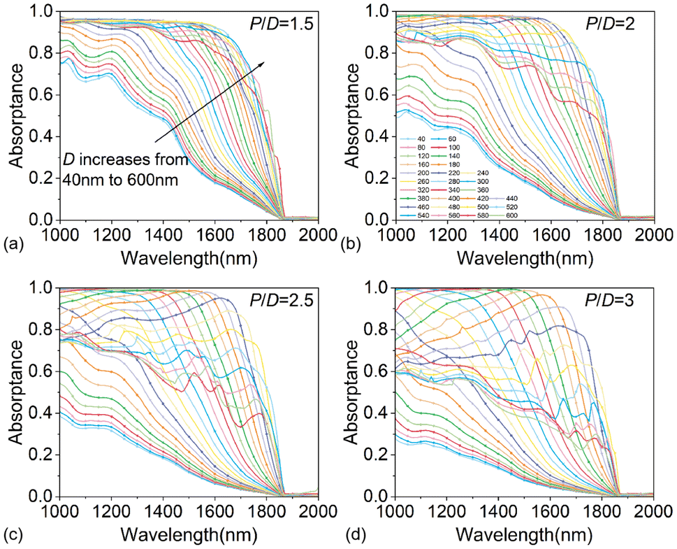 | ||
| Fig. 5 (a)–(d) Absorptance with the variation of P/D ranging from 1.5 to 3 for the NW array of length H = 3 μm for TE-polarized light. | ||
Additionally, for each P/D ratio, the absorptance versus D is also depicted. As the diameter increases, the absorptance initially increases, followed by saturation and eventually decreases rapidly. The absorptance of NW arrays with extremely small or large diameters has a narrow wavelength range capable of near-complete absorptance. Taking P/D = 2.5 as an example, when the diameter of the NW is small (<260 nm), the enhancement of absorptance is mainly due to the enhanced resonance caused by the increase in diameter. As the diameter gets large, the absorptance peak caused by LMR exhibits a continuous redshift. The abrupt decline in absorption observed in the NW array can be attributed to the enhanced transmission at longer wavelengths and increased reflection off the top, both of which are consequences of the greater diameter (>460 nm) of the array.
To be specific, the P/D ratio determines the overall absorptance, whereas the diameter D dominates the peak and mostly influences the wavelength at which peak absorptance occurs. Thus, to achieve optimal absorptance, it is imperative to meticulously tune the size of NWs and the arrangement of their arrays.
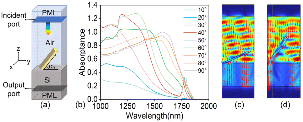
In contrast to cylindrical NWs, hexagonal NWs exhibit a distinct six-fold symmetry, which leads to variations in light absorption characteristics at different incident angles. The absorptance at various elevation angles α1 was initially computed, as α1 is determined from the angle formed between the outward unit normal vector to the boundary n and the incoming wave vector k, as depicted in Fig. 4(a). The angle of 0° denotes a scenario where light is incident vertically, whereas an angle of 90° signifies light incident in the x-direction at the uppermost part of the air layer. When the incidence elevation angle is below 40°, it is observed that the absorptance can surpass 95% across a broad range of wavelengths, while for α1 between 40° and 65°, the absorptance is as high as 90%, as seen in Fig. 6(a). As α1 increases, there is a corresponding redshift observed in the absorption peak at the longer wavelength. When the α1 exceeds 75°, the absorptance decreases rapidly. The optical power loss spectrum and the Poynting vector of different angles α1 at 1400 nm are shown in Fig. 6(c)–(e).
 | ||
| Fig. 6 (a) Absorptance as a function of wavelength and elevation angle α1. (b) Absorptance as a function of wavelength and azimuth angle α2 when α1 is set to 40°. (c)–(e) The optical power loss spectrum and the Poynting vector of different angles α1 at 1400 nm. (f)–(k) The optical power loss spectrum and the Poynting vector of different angles α2 at 1200 nm and 1400 nm. | ||
Subsequently, theoretical calculations were performed to determine the impact of varying azimuth angles α2 on the absorptance of NW arrays, assuming a fixed incident elevation angle α1 of 40°. α2 denotes the angle formed between the incident light and the axis while rotating within the x–y plane. An angle of 0° indicates a line parallel to the x-axis, whereas an angle of 90° degrees indicates a line parallel to the y-axis. Considering the symmetry of the hexagon, the analysis exclusively encompassed azimuth angles within the range of 0°–90°. The results are shown in Fig. 6(b). Almost all incident azimuths exhibit an absorptance of over 90% throughout the entire spectral range of concern. Due to the symmetry of the regular hexahedron, the absorptance also exhibits symmetry about 45°, with the 0° absorptance curve similar to that of 90° and the 10° absorption curve resembling that of 80° and so on. In the spectral range below 1350 nm, the absorptance exhibits the lowest efficiency when the α2 is 45°. This can be mainly attributed to the high reflectance of the incident light at 45° and the subsequent emission of NWs. These processes contribute to an overall rise in the total reflectivity of the NW array. Fig. 6(f)–(h) depict the optical power loss spectrum and Poynting vector of the x–y plane situated at the uppermost region of the NW, specifically at α2 equal to 20°, 40°, and 60° at a wavelength of 1200 nm. The optimal absorptance is achieved when α2 is set at 45° beyond the wavelength of 1350 nm. As seen in Fig. 6(i)–(k), the absorptance predominantly occurs at the core position, primarily attributed to the enhanced penetration of long wavelength light within the NW. Currently, the incidence azimuth angle α2 of 45° experiences a reduced impact from refraction, resulting in a higher absorption of photons.
Inclined InN NW arrays
Furthermore, the optical pathway can be extended by enhancing the reflection among the NW arrays, hence boosting the absorption, expanding methods to enhance absorption, and adjusting their dimensions and distributions to achieve higher absorption intensity. When NWs are aligned axially in parallel with the direction of light incidence and perpendicular to the substrate, a substantial proportion of the incident light is reflected toward air, while just a fraction of the photons that undergo refraction and reflection along the sidewalls of NWs has the possibility to be secondarily absorbed. One practical approach for expanding the optical pathway is accomplished by tilting the NWs at an angle relative to the substrate. Etching has been reported as an optional method to fabricate inclined Si NWs,45 while previous theoretical studies have also demonstrated that the inclined Si and GaAs NWs demonstrate enhanced absorption compared to perpendicular NWs.46,47Fig. 7(a) illustrates the schematic diagram of periodic inclined NWs, characterized by a diameter of 400 nm and a length of 3 μm. The inclination angle α3, denoted as the angle between the NW and the substrate, is defined as 90°, indicating a perpendicular orientation to the substrate, while 0° indicates the NW lying entirely flat. The resulting absorptions of InN NWs depend on the different α3 displayed in Fig. 7(b). The absorption in the theoretical simulation falls significantly below 100%, ascribed to their P/D ratio being considerably lower than the ideal value of 2.5. To intuitively illustrate how inclined NWs can affect absorption, the maximal absorption of the vertical NW arrays in SWIR is normalized for all other inclined NWs. The absorption effect of tilted NWs can increase the absorption rate by a further 28%.
 | ||
| Fig. 7 (a) The periodic model of the inclined InN NW array. (b) The absorption spectrum of the NW array is dependent on the inclination angle α3 under TE-polarized light. The cross-section of distribution of the electric field intensity |E| inside the inclined InN NW under TE-polarized incidence at λ = 1300 nm: (c) α3 = 20° and (d) α3 = 50°. | ||
The NWs that possess minor α3 from 10° to 20° show much lower absorption than vertical NWs, as the diameters of these near-lying flat NWs determine the absorbed length of the incident light, which is insufficient to absorb light. Compared to shorter wavelengths, the distribution of the electric field intensity |E| is predominantly localized near the border at longer wavelengths, as depicted in Fig. 7(c). Hence, the absorptance at longer wavelengths is comparatively lower than that at shorter wavelengths, consistent with Fig. 3(a). The absorption characteristics of NWs with an α3 ranging from 30° to 50° exhibit enhanced absorptions compared to the vertical ones. The absorption intensities exhibit a progressive augmentation and red-shift with the elevation of α3. The observed phenomenon can be explained by the guided-mode-fiber function of these inclined NWs, in which incident light simultaneously absorbs and undergoes multiple reflections within NWs’ sidewalls. At an α3 of 50°, the number of photons that are reflected subsequently increases due to the propagation of reflected light along the axis of NWs. Thus, the maximum absorption is obtained at a wavelength of about 1330 nm, as depicted in Fig. 7(d). With a further increase in α3, the projection area of the NWs on the substrate diminishes, leading to a reduction in the number of acceptable incident photons. Consequently, the absorption within the SWIR wavelength range experiences a decline. However, NWs with an inclination angle α3 ranging from 30° to 70° exhibit a distinct peak at around 1560 nm, which can be attributed to the resonance effect between the inclined NWs and the refraction and reflection of the incident light. The cross-sectional distribution of the electric field intensity |E| inside an inclined InN nanowire with α3 = 50° is taken as an example, as shown in Fig. S4.† Thus, it has been established that manipulating the inclined angle of the NWs while simultaneously ensuring the suitable dimensions and arrangement of the NW arrays can effectively modulate the absorption.
Comparison with InGaAs NWs
Having optimized the NWs based on their optical absorption performance, further simulations of their photoelectric properties were conducted utilizing the refined periodic structure seamlessly integrated onto a silicon substrate. The doping configuration of the repeating InN NW unit, as depicted in Fig. 8(a), incorporates a P-type ohmic contact at the apical end and an N-type ohmic contact at the base interface with Si, resulting in the formation of an efficient PIN structure within the NWs. The incident light direction is perpendicular to the substrate and parallel to the NW direction with the power set to 1 mW. | ||
| Fig. 8 (a) The doping configuration of the repeating NW unit in periodic arrays. Red represents n-type doping and blue represents p-type doping. (b) The responsivity curve of InN and the InGaAs NW array within the SWIR range. | ||
The responsivity curve of the InN NW array within the SWIR range is presented in Fig. 8(b), achieving a remarkable responsivity of ∼1 A W−1 at 1550 nm wavelength and the maximum responsivity can reach up to 1.16 A W−1 at 1730 nm. This finding underscores the potential of InN NW arrays as highly effective photodetectors.
For a comprehensive comparison, the responsivity data of InGaAs NW arrays with identical nanostructures and doping configurations were also included, which are also presented in Fig. 8(b). Notably, the InGaAs NWs exhibit a lower responsivity of 0.89 A W−1 at 1550 nm with a maximum responsivity of 0.93 A W−1, further validating the superior performance of the InN NW arrays. Table 1 presents the optical absorptance performance of InGaAs and InN NW arrays at 1550 nm with the same size.
| InN | InGaAs | |
|---|---|---|
| Absorption coefficient (cm−1) | 1.40 × 10⁴ | 0.19 × 10⁴ |
| Light absorption coefficient | 99.82% | 90.18% |
| Responsivity (A W−1) | 0.99 | 0.89 |
Conclusions
In summary, we have proven that the III–V NW arrays made of InN semiconductors are highly promising photosensitive materials in the SWIR range due to their outstanding light absorption properties. Our calculation shows that the subwavelength dimensions, high refractive index and high absorption coefficient of InN NWs enable them to absorb light beyond their projected area and sustain multiple enhancement light absorption modes, resulting in approximately 99% light absorption ability performance in the wide 1000–1470 nm range and incidence angles (0–65°). By adjusting the size, height, arrangement, and tilt angle of the NW arrays, even with a relatively low filling ratio and height, it is possible to achieve light absorption 28% higher than that of bulk devices with the same height. By adopting precisely optimized NW arrays, a response rate as high as 1 A W−1 can be achieved at 1550 nm wavelength by InN, which is 11.83% higher than that of InGaAs. Meanwhile, the maximum optical response in the SWIR range is 24.73% higher than that of InGaAs NW arrays. Our newly gained understanding of absorption features in individual NWs and NW arrays can now guide the rational design of high-efficiency NW-based photodetectors or photovoltage cells that can operate at high temperature.Data availability
The authors confirm that the data supporting the findings of this study are available within the article and its ESI.†Conflicts of interest
There are no conflicts to declare.Acknowledgements
This work was supported by the National Natural Science Foundation of China (Award/grant Number : 62474163), National Natural Science Foundation of China (Award/grant Number :U24A20318), Natural Science Foundation of Zhejiang Province (Award/grant Number : Z24F040009), Natural Science Foundation of Zhejiang Province (Award/grant Number : LZ24F040001), Qizhen Program of Zhejiang University (Award/grant Number : K20240015), Special Fund for Innovative Development of Hangzhou Chengxi Science and Technology Innovation Corridor (Award/grant Number : 226-2024-00050) and Youth Special Project of Zhejiang University of Integrated Circuits School.References
- I. Grzegory, J. Jun, S. Krukowski, P. Perlin and S. Porowski, InN Thermodynamics and Crystal Growth at High Pressure of N2, Jpn. J. Appl. Phys., 1993, 32, 343 CrossRef.
- V. Kumar and D. R. Roy, Structure, bonding, stability, electronic, thermodynamic and thermoelectric properties of six different phases of indium nitride, J. Mater. Sci., 2018, 53, 8302–8313 CrossRef.
- S. Adachi, Optical dispersion relations for GaP, GaAs, GaSb, InP, InAs, InSb, AlxGa1−xAs, and In1−xGaxAsyP1−y, J. Appl. Phys., 1989, 66, 6030–6040 CrossRef.
- T. N. Nunley, et al., Optical constants of germanium and thermally grown germanium dioxide from 0.5 to 6.6eV via a multisample ellipsometry investigation, J. Vac. Sci. Technol., B: Nanotechnol. Microelectron.: Mater., Process., Meas., Phenom., 2016, 34 DOI:10.1116/1.4963075.
- S. Zhao and Z. Mi, InN Nanowires: Epitaxial Growth, Characterization, and Device Applications, 2017, pp. 267–304 Search PubMed.
- S. K. O’Leary, B. E. Foutz, M. S. Shur and L. F. Eastman, Steady-state and transient electron transport within bulk wurtzite indium nitride: An updated semiclassical three-valley Monte Carlo simulation analysis, Appl. Phys. Lett., 2005, 87 DOI:10.1063/1.2135876.
- R. Ascázubi, I. Wilke, K. Denniston, H. Lu and W. J. Schaff, Terahertz emission by InN, Appl. Phys. Lett., 2004, 84, 4810–4812 CrossRef.
- J. Jia, T. Yagi and T. Makimoto, Ultrafast dynamics of electronic structure in InN thin film, 2021 Search PubMed.
- K. Ghosh and U. Singisetti, Design and Analysis of High Frequency InN Tunnel Transistors, 2013 Search PubMed.
- F. Gucmann, et al., InN crystal habit, structural, electrical, and optical properties affected by sapphire substrate nitridation in N-polar InN/InAlN heterostructures, Semicond. Sci. Technol., 2021, 36, 075025 CrossRef.
- K. S. A. Butcher and T. L. Tansley, InN, latest development and a review of the band-gap controversy, Superlattices Microstruct., 2005, 38, 1–37 CrossRef.
- G. Motlan, E. M. Tansley and T. L, Optical and electrical properties of InN grown by radio-frequency reactive sputtering, J. Cryst. Growth, 2002, 241, 165–170 CrossRef.
- J. Wu, et al., Unusual properties of the fundamental band gap of InN, Appl. Phys. Lett., 2002, 80, 3967–3969 CrossRef.
- Y. Nanishi, Y. Saito and T. Yamaguchi, RF-Molecular Beam Epitaxy Growth and Properties of InN and Related Alloys, Jpn. J. Appl. Phys., 2003, 42, 2549–2559 Search PubMed.
- B. A. Andreev, et al., Towards the indium nitride laser: obtaining infrared stimulated emission from planar monocrystalline InN structures, Sci. Rep., 2018, 8, 9454 Search PubMed.
- D.-J. Jang, et al., Carrier dynamics and intervalley scattering in InN, Opt. Mater., 2009, 31, 1857–1859 CrossRef.
- Y. Wang, N. Guan, J. Yu and H. Li, Research on Transmission Rate of Deep Space Optical Communications Based on PPM Technology, in 2022 2nd International Conference on Consumer Electronics and Computer Engineering (ICCECE), IEEE, 2022, pp. 356–359.
- E. Farooq, A. Sahu and S. K. Gupta, Survey on FSO Communication System—Limitations and Enhancement Techniques, 2018, pp. 255–264 Search PubMed.
- R. D. Esman, P. D. Biernacki, L. T. Nichols and P. J. Matthews, Optoelectronics for radio frequency conversion. in Conference Proceedings, LEOS'98. 11th Annual Meeting, IEEE Lasers and Electro-Optics Society 1998 Annual Meeting (Cat. No.98CH36243), IEEE, vol. 2, pp. 253–254.
- G.-O. Glentis, et al., Cost-effective adaptive optical network technologies for Metropolitan Area Networks, in 2014 16th International Conference on Transparent Optical Networks (ICTON), IEEE, 2014, pp. 1–4.
- Z. C. Feng, et al., Optical, surface, and structural studies of InN thin films grown on sapphire by molecular beam epitaxy, J. Vac. Sci. Technol., A, 2023, 41 DOI:10.1116/6.0002665.
- W.-C. Chen, et al., Study of InN epitaxial films and nanorods grown on GaN template by RF-MOMBE, Nanoscale Res. Lett., 2012, 7, 468 Search PubMed.
- W. Wang and G. Zhao, Lattice vibrations and optical properties of wurtzite InN in the reststrahlen region, Physica B: Condens. Matter, 2012, 407, 4313–4317 CrossRef.
- F. Gao, et al., Growth of InN Nanowires with Uniform Diameter on Si(111) Substrates: Competition Between Migration and Desorption of In Atoms, Small, 2017, 13 DOI:10.1002/smll.201603775.
- C. Honsberg, A. Barnett and D. Kirkpatrick, Nanostructured Solar Cells for High Efficiency Photovoltaics, in 2006 IEEE 4th World Conference on Photovoltaic Energy Conference, IEEE, 2006, pp. 2565–2568.
- R. R. LaPierre, Numerical model of current-voltage characteristics and efficiency of GaAs nanowire solar cells, J. Appl. Phys., 2011, 109 DOI:10.1063/1.3544486.
- L. Wen, et al., Theoretical analysis and modeling of light trapping in high efficicency GaAs nanowire array solar cells, Appl. Phys. Lett., 2011, 99 DOI:10.1063/1.3647847.
- E. Garnett and P. Yang, Light Trapping in Silicon Nanowire Solar Cells, Nano Lett., 2010, 10, 1082–1087 CrossRef CAS PubMed.
- Y. Guan, G. Cao and X. Li, Single-nanowire silicon photodetectors with core-shell radial Schottky junction for self-powering application, Appl. Phys. Lett., 2021, 118 DOI:10.1063/5.0046096.
- L. Hu and G. Chen, Analysis of Optical Absorption in Silicon Nanowire Arrays for Photovoltaic Applications, Nano Lett., 2007, 7, 3249–3252 Search PubMed.
- L. Liu, et al., Absorption and photoemission of optically localized GaN nanowire array cathode, MRS Commun., 2023, 13, 162–168 Search PubMed.
- Y. Berdnikov, et al., Mapping of Fabry–Perot and whispering gallery modes in GaN microwires by nonlinear imaging, Nanotechnology, 2021, 32, 40LT01 CrossRef CAS PubMed.
- L. Cao, et al., Semiconductor Nanowire Optical Antenna Solar Absorbers, Nano Lett., 2010, 10, 439–445 Search PubMed.
- T. J. Kempa, et al., Coaxial multishell nanowires with high-quality electronic interfaces and tunable optical cavities for ultrathin photovoltaics, Proc. Natl. Acad. Sci. U. S. A., 2012, 109, 1407–1412 CrossRef CAS.
- M. Aghaeipour and H. Pettersson, Enhanced broadband absorption in nanowire arrays with integrated Bragg reflectors, Nanophotonics, 2018, 7, 819–825 CAS.
- N. Anttu and H. Q. Xu, Coupling of Light into Nanowire Arrays and Subsequent Absorption, J. Nanosci. Nanotechnol., 2010, 10, 7183–7187 CrossRef CAS PubMed.
- J. Furthmüller, P. H. Hahn, F. Fuchs and F. Bechstedt, Phys. Rev. B, 2005, 72, 205106 Search PubMed.
- S. Mokkapati and C. Jagadish, Review on photonic properties of nanowires for photovoltaics [Invited], Opt. Express, 2016, 24, 17345 CrossRef CAS.
- Z. Li, et al., Review on III–V Semiconductor Nanowire Array Infrared Photodetectors, Adv. Mater. Technol., 2023, 8 DOI:10.1002/admt.202202126.
- A. Mukherjee, et al., GaAs/AlGaAs Nanowire Array Solar Cell Grown on Si with Ultrahigh Power-per-Weight Ratio, ACS Photonics, 2021, 8, 2355–2366 Search PubMed.
- D. Li, et al., A supersensitive silicon nanowire array biosensor for quantitating tumor marker ctDNA, Biosens. Bioelectron., 2021, 181, 113147 CrossRef CAS PubMed.
- B. Tekcan, et al., Semiconductor nanowire metamaterial for broadband near-unity absorption, Sci. Rep., 2022, 12, 9663 Search PubMed.
- N. Yulianto, et al., Wafer-scale transfer route for top–down III-nitride nanowire LED arrays based on the femtosecond laser lift-off technique, Microsyst. Nanoeng., 2021, 7, 32 CrossRef CAS PubMed.
- K. M. Azizur-Rahman and R. R. LaPierre, Wavelength-selective absorptance in GaAs, InP and InAs nanowire arrays, Nanotechnology, 2015, 26, 295202 CrossRef CAS PubMed.
- X. Meng, et al., Stable Superwetting Surface Prepared with Tilted Silicon Nanowires, Nano-Micro Lett., 2016, 8, 388–393 CrossRef.
- Z. Kordrostami and H. Sheikholeslami, Optimization of light trapping in square and hexagonal grid inclined silicon nanowire solar cells, Opt. Commun., 2020, 459, 124980 CrossRef CAS.
- M. Zamani, Z. Kordrostami and S. Hamedi, Efficient inclined core-shell nanowire solar cells, Optik, 2021, 248, 167974 CrossRef CAS.
Footnote |
| † Electronic supplementary information (ESI) available. See DOI: https://doi.org/10.1039/d4nr04586f |
| This journal is © The Royal Society of Chemistry 2025 |