
Reinforcing built-in electric field to enable efficient carrier extraction for high-performance perovskite solar cells
Jiahui
Cheng
,
Huijie
Cao
,
Shuming
Zhang
,
Fang
Yue
* and
Zhongmin
Zhou
 *
*
College of Chemistry and Molecular Engineering, Qingdao University of Science and Technology, Qingdao 266042, China. E-mail: fangyue@qust.edu.cn; zhouzm@qust.edu.cn
First published on 28th November 2023
Abstract
Perovskite solar cells (PSCs) have gained significant attention in recent years due to their low fabrication cost, solution-based processing, potential for flexibility and large-scale solar energy conversion. The performance of PSCs depends on effectively separating and collecting the photogenerated charge carriers before they recombine and lose excess energy. Therefore, efficient carrier extraction is crucial for achieving high-performance PSCs. The built-in electric field (BEF) within PSCs serves as the driving force for extracting carriers to their corresponding electrodes. Reinforcing the BEF can reduce carrier recombination in the bulk phase/interface, facilitate carrier separation and extraction, and minimize energy losses in PSCs. Up to now, numerous efforts have been made to enhance the BEF and further improve the photovoltaic performance of PSCs. This review first describes the carrier separation and extraction mechanism influenced by the BEF. It then summarizes various strategies used to enhance the BEF in PSCs, including forming semiconductor junctions, regulating energy levels through dipole layers and functional layer modifications, constructing a ferroelectricity polarization electric field (PEF) within PSCs, and mitigating the surface charge accumulation caused by ion migration. Finally, this review discusses the prospects for designing an enhanced BEF to promote the continuous development of high-performance PSCs. This review provides useful insights for further analyzing the mechanism of the BEF in PSCs and achieving breakthroughs in the efficiency of PSC devices through field effect passivation.
 Jiahui Cheng | Jiahui Cheng is currently a postgraduate majoring in chemistry at Qingdao University of Science and Technology under the supervision of Prof Zhongmin Zhou. His research fields are ferroelectric materials and perovskite solar cells. |
 Huijie Cao | Huijie Cao is currently a postgraduate in chemistry at Qingdao University of Science and Technology under the supervision of Prof Zhongmin Zhou. She received her BS degree (2022) in chemistry from Qingdao University of Science and Technology. Her current research focuses on efficient tin-lead perovskite solar cells. |
 Shuming Zhang | Shuming Zhang is currently a graduate student majoring in chemistry at Qingdao University of Science and Technology. In 2022, he received a bachelor of science degree from Qingdao University of Science and Technology. His research mainly focuses on tin-lead perovskite solar cells. |
 Fang Yue | Fang Yue is currently an associate professor at Qingdao University of Science and Technology. She received her PhD degree from the School of Chemistry and Chemical Engineering, Shandong University, in 2019, and then conducted her postdoctoral research at the Key Laboratory of Advanced Energy Materials Chemistry in Nankai University. Her research interests include perovskite solar cells and the design of rechargeable aqueous batteries. |
 Zhongmin Zhou | Zhongmin Zhou is currently a professor at Qingdao University of Science and Technology. He received his PhD degree from the Institute of Chemistry, Chinese Academy of Sciences (CAS), in 2014, and then conducted postdoctoral research at CAS – Qingdao Institute of Bioenergy and Bioprocess Technology, National Institute of Materials Science (NIMS), and The University of Tokyo. His research interest is functional materials and devices. |
1. Introduction
In recent years, influenced by the energy demand and environmental issue policies of countries around the world, the development of renewable and environment-friendly energy technologies has become a research priority in various countries. Photovoltaic technologies can directly convert solar energy into electricity by using photovoltaic devices, which have the potency to address the issue of energy crisis and environmental contamination. Among the various photovoltaic devices, perovskite solar cells (PSCs) are considered to be a promising candidate for next-generation photovoltaic cells due to their high power conversion efficiencies (PCE) and low-cost fabrication processes, benefiting from the distinctive merits of perovskite materials, including high charge carrier mobility, low exciton binding energy, easily tunable bandgap, long carrier diffusion length, and high absorption coefficient.1–5 In addition, the solution-processable fabrication at low temperature and affordable cost of materials makes PSCs convenient for achieving flexibility and large-scale application.6 In 2009, perovskite materials were used as sensitizers in dye-sensitized solar cells for the first time and a PCE of 3.8% was obtained.7 To date, the highest certified PCE of PSCs has reached 26.1%,8 benefiting from the intense efforts to develop novel device architectures and regulate the crystallization of perovskite materials. However, the certified efficiency is still below the Shockley–Queisser (S–Q) limit of single-junction solar cells.9 Therefore, the efficiency of PSCs has enormous potential to further increase with fast speed.In principle, the high efficiency of PSCs strongly depends on the efficient separation and extraction of photogenerated charge carriers to the corresponding electrodes. The built-in asymmetry arising from appropriate contacts in photovoltaic devices creates a driving force for carrier extraction. Commonly, the perovskite photoactive absorbing layer absorbs the energy of light and then produces electron–hole pairs (e–h pairs). Owing to the weak exciton binding energy, the e–h pairs are easily separated and migrate directionally under the driving force, and are subsequently extracted at the negative and positive poles through the electron transport layer (ETL) and the hole transport layer (HTL), respectively.10 There are two main mechanisms for charge extraction in solar cells, including diffusion and drift.11 The charge extraction mechanism based on diffusion is reliant on the establishment of kinetic selectivity at the contacts and long carrier diffusion length of the active layer.12 As for the drift-based mechanism, the charge extraction is driven by the built-in electric field (BEF). It is necessary to establish a drift–diffusion model to study the carrier separation mechanism in PSCs. In the diffusion-dominated PSC model, the BEF is not the main driving force for carrier separation. The selective contact of interface can ensure the effective extraction of the diffusion-driven carriers, but the BEF is still an important driving force for the directional transport of carriers.13,14 Therefore, an in-depth understanding of the source and mechanism of the BEF in PSCs is a prerequisite for obtaining high-performance PSCs. This BEF is mainly determined by the difference in work functions (WFs) between two electrodes or charge transport layers.15 In general, PSCs are composed of a perovskite layer sandwiched between the HTL and the ETL. The difference in the majority carrier concentration results in the formation of a space charge region (depletion region) near the interface between the perovskite layer and the transport layer, which produces a BEF. Under the action of the BEF, the photogenerated carriers can realize directional drift and give rise to a photocurrent. Moreover, a built-in potential arising from the BEF could avoid forming a reverse electric field inside the active layer, which will ensure efficient charge extraction through the ETL/HTL.12
It has been well recognized that the serious charge recombination at the perovskite bulk and interface hinders the efficient charge extraction and thus restricts further improvement of the device performance.16 Generally, perovskite films prepared by a simple solution method are polycrystalline, which induces inevitable structural defects at grain boundaries (GBs). These structural defects can serve as non-radiative recombination centers for photogenerated carriers, which will cause severe non-radiative recombination and energy loss. Maintaining the advantage of facile fabrication of PSCs and minimizing the energy loss require more effort. Besides the defect passivation strategy, regulating the internal driving force for carrier separation and transmission has been developed to solve this problem.17–23 For PSCs, the existence of the BEF can reduce the possibility of charge carriers being trapped by defects and help the trapped charge carriers escape.24,25
In view of the important role of the BEF in the process of carrier separation, extraction and transport in PSCs, the intensity of the BEF is directly related to the performance of PSCs.26 In previous studies, many strategies to enhance the BEF have been proposed. For example, constructing p–n junctions or heterojunctions in the perovskite layer or at the perovskite/transport layer interface can increase additional depletion regions, resulting in an enhanced BEF in PSCs.27,28 Introducing a dipole layer at the interface to regulate the WF of the functional layer also can be used to increase the BEF.29 Furthermore, designing a ferroelectric intermediate layer of two-dimensional (2D) perovskites or introducing ferroelectric materials can form an additional polarization electric field (PEF) which promotes charge extraction and thus improves the performance of PSCs.30
Although significant effort has been made in the design of an enhanced BEF and high-performance PSCs, there is still a lack of a comprehensive review that summarizes these strategies through the core point of the BEF. In this review, we briefly introduce the carrier separation and extraction mechanism affected by the BEF and the distribution of the BEF in PSCs. Then, we summarize the strategies proposed in the past few years to enhance the BEF (Fig. 1), which are divided into four parts: constructing junctions in PSCs, regulating the energy level, constructing the PEF and mitigating charge accumulation caused by ion migration. Finally, we discuss the problems existing in the BEF regulation strategy and look forward to the prospect of BEF enhancement for the development of high-performance PSCs.
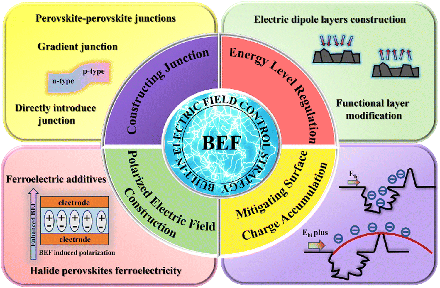 | ||
| Fig. 1 Schematic diagram of BEF regulation. | ||
2. Built-in electric field in PSC devices
Any PSC architecture undergoes the same basic process of energy conversion, that is, the light absorption layer of the solar cell absorbs sunlight and then triggers the generation, separation, and transmission of charge carriers and their collection at the corresponding electrode.31–34 Fundamentally, the device performance of PSCs mainly depends on the capture of light with different wavelengths by the perovskite absorbing layer and the separation and extraction of photo-generated charge carriers. Among them, efficient charge separation and extraction would ensure the effective operation of PSCs.The typical device structures of PSCs can be categorized into two main types: mesoporous and planar structures. The latter also includes regular n–i–p and inverted p–i–n devices, where n, i, and p represent the ETL, the perovskite layer, and the HTL, respectively.32 The sandwich structure of PSCs endows them with excellent interface selective contact. The BEF is formed near the interface, which can drive the directional movement of charge carriers. In fact, the BEF arises from the difference of WFs between the two contacts. This established BEF would provide a driving force for interfacial electron–hole separation and their extraction to the corresponding electrodes to create photocurrent. Furthermore, the deep-level defects in the bulk perovskite layer and the interface between the perovskite layer and the transport layer can form harmful non-radiative recombination centers, leading to serious energy loss. A strong BEF is sufficient to support the escape of photogenerated excitons in deep-level defects. In addition, the BEF is often directly related to the VOC of PSCs.35 Therefore, the related fundamental understanding of the BEF is necessary for elucidating the working principle of PSCs and further optimizing their performance.36–38
To study the separation and extraction mechanism of carriers affected by the BEF, it is crucial to pinpoint the location of BEF distribution and its intensity in PSCs. Eddi et al. used electron beam-induced current (EBIC) technology and cross-sectional SEM to plot the changes of the current amplitude generated in the device in cross-section, which is useful for locating the driving force for charge separation and thus analyzing the working principle of PSC devices.31 In principle, e–h pairs are generated when a scanning beam of electrons is directed toward the light absorbing layer. In the presence of a driving force for charge separation and contacts to collect the charge carriers, a current is generated in the form of an EBIC signal. The intensity of the EBIC signal indicates the efficiency of charge separation and collection. The results show that there exist two main efficient carrier separation positions (Fig. 2): one near the absorber/hole barrier layer and the other near the absorber/electron barrier layer interface. This “bimodal” structure is a feature of p–i–n solar cells, which contain a semiconductor absorber layer with low doping and high electron quality between the p- and n-layers.
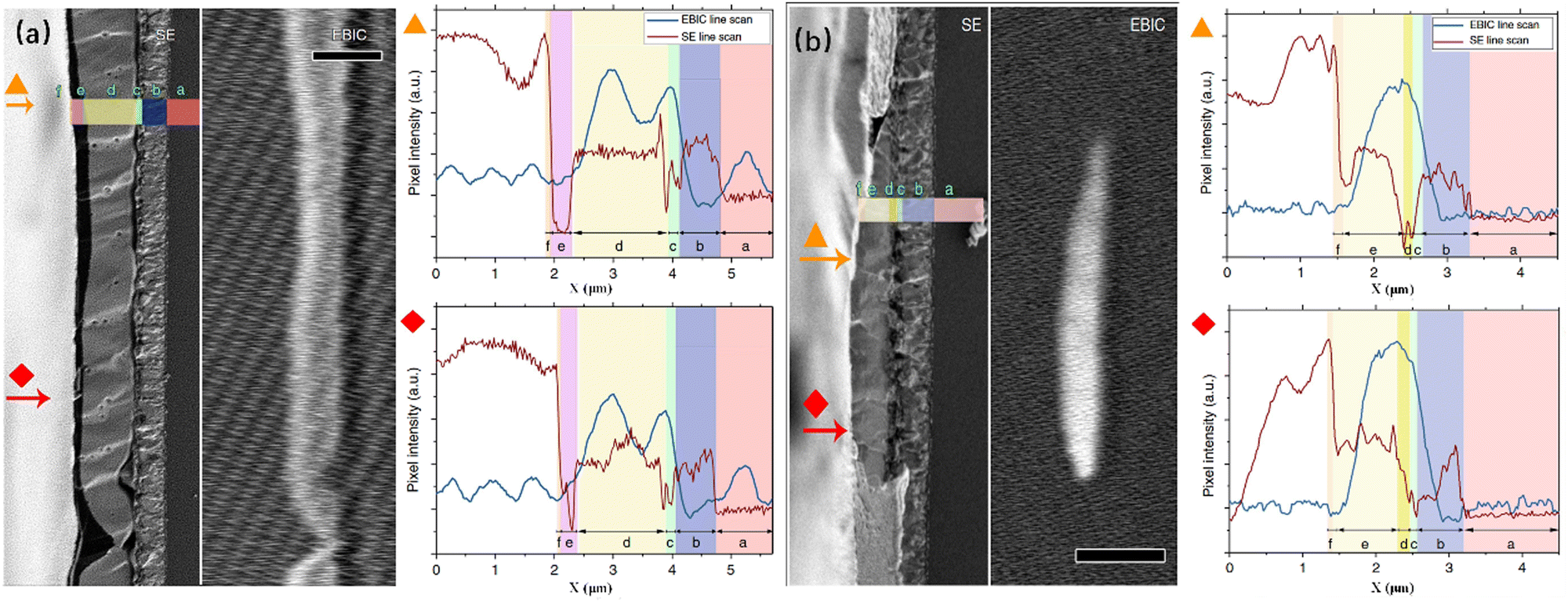 | ||
| Fig. 2 (a) EBIC characterization of a flat CH3NH3PbI3−xClx device with hole transporting material (HTM). SE image and corresponding EBIC image of a cross-section of a solar cell without mesoporous alumina. Left, SE image; right, EBIC image. (b) EBIC characterization of a CH3NH3PbI3−xClx device with a thin mesoporous-Al2O3 without HTM. SE image and corresponding EBIC image of a cross-section of a solar cell with a thin mesoporous-Al2O3 and without HTM. Left, SE image; right, EBIC image.31 Copyright 2014, Springer Nature. | ||
Since EBIC measurement is based on the local excitation and extraction of charge carriers by an electron beam, it cannot truly simulate solar cells under normal operating or dark conditions. The potential distribution of PSCs measured based on EBIC is inaccurate and speculative. The potential distribution in PSCs can be directly detected by Kelvin probe force microscopy (KPFM) by detecting the contact potential difference (CPD) between the needle tip and the sample using a probe. In addition, the KPFM measurement method obtains nano-resolution imaging through a local contact, which is more advantageous in exploring the potential distribution of PSCs.39–43 The mechanisms of EBIC and KPFM are described in Fig. 3.
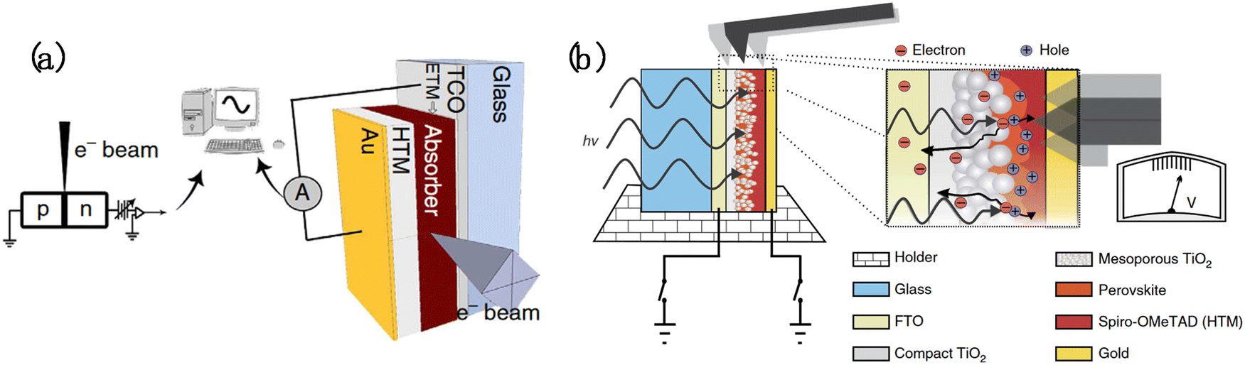 | ||
| Fig. 3 (a) Illustration of an EBIC experiment on a cross-section of a thin-film solar cell. The electron beam generates e–h pairs in the absorber material, which, after separation, creates a current generation profile inside the cell. TCO, transparent conducting oxide; ETM, electron transporting materials.31 Copyright 2014, Springer Nature. (b) Schematic diagram of the KPFM measurement principle.42 Copyright 2014, Springer Nature. | ||
Based on the KPFM measurement, Bergmann et al. studied the real spatial cross-sectional distribution of internal potential in high-efficiency mesoporous perovskite solar cells, which proved that the electric field in PSCs is uniform. However, the charge transfer is imbalanced under lighting conditions. Electron extraction is faster than hole extraction, leading to hole accumulation at the interface between the perovskite layer and the HTL. Such hole accumulation results in the formation of a potential barrier in the front of the HTL, which will reduce JSC in PSCs.42
Furthermore, Cai et al. studied the control of the potential distribution in high-performance PSCs through KPFM technology.44 They prepared p-type (rich-MAI) and n-type (rich-PbI2) perovskite devices to investigate the effect of semiconductor doping type on the formation of diode junctions in PSCs. As shown in KPFM (Fig. 4), there is a diode junction and significant potential drop between mesoporous-TiO2 and perovskite film in mesoporous-TiO2 structured PSCs, where the main charge separation occurred. Meanwhile, this diode junction is almost unaffected by the self-doping of the perovskite layer. In addition, there are two diode junctions near the perovskite/HTL and perovskite/ETL interfaces in planar PSCs, which are affected by the doping of perovskite layers. The mechanism of the BEF in PSCs can be better understood by determining the number, position, and intensity of junctions in PSCs through measuring the potential distribution and potential changes.
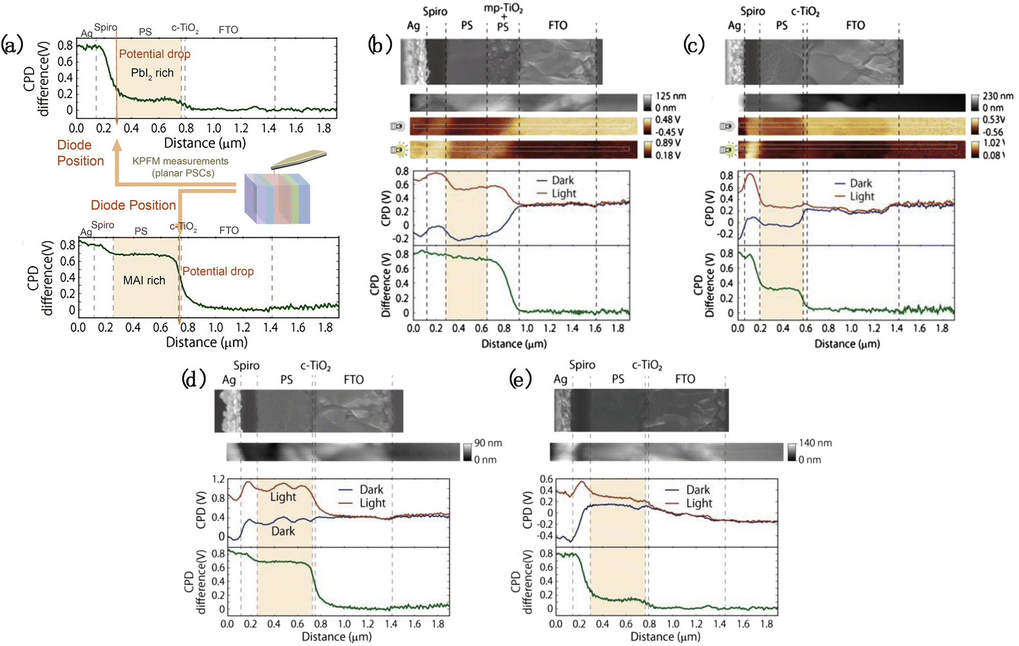 | ||
| Fig. 4 (a) KPFM measurements of planar PSCs. (b) and (c) KPFM characterization of the mesoporous type PSCs fabricated using MAI- and PbI2-rich precursors. (d) and (e) KPFM characterization of the planar type PSCs fabricated using MAI- and PbI2-rich precursors.44 Copyright 2018, Elsevier. | ||
3. Design strategies for enhancing the built-in electric field of perovskite solar cells
The BEF in PSCs provides a vital driving force for the separation and extraction of photogenerated charge carriers, which have a significant effect on the photovoltaic performance of PSCs. A strong BEF could facilitate efficient charge extraction to the corresponding electrodes and avoid charge recombination in the active layer. Thus, it is important to enhance the BEF for high efficiency of PSCs. In this section, the design strategies for enhancing the BEF and their influence on the performance of PSCs will be introduced in detail. These strategies consist of four main approaches: constructing junctions, regulating the energy level, constructing a ferroelectricity polarized electric field, and mitigating surface charge accumulation caused by ion migration.3.1. Constructing junctions
Perovskite solar cells possess junction characteristics. Shi et al. confirmed that the TiO2/CH3NH3PbI3/Au solar cell is a typical heterojunction solar cell by using the ideal current–voltage model of single heterojunction solar cells in PSCs without a hole layer.45 Since then, the strategies for the construction and enhancement of junctions in PSCs have been explored. Previous studies on the potential distribution in PSCs have shown that there are one or two junctions in PSCs depending on their structural framework (mesoporous or planar structure). The position of the junctions of PSCs is usually near the interface, and the BEF is generated in the junctions. The intensity of the intrinsic BEF depends on the thickness of the space charge layer (depletion layer) formed near the interface.The p–n junction is a frequently mentioned concept in semiconductor physics and is widely applied in conventional solar cells. Constructing additional p–n junctions in PSCs is a common strategy to enhance the BEF. In general, the majority of carriers of n-type semiconductors are electrons, and the majority of carriers of p-type semiconductors are holes. Thus, the difference in concentration would drive the majority of carriers to the low-concentration region when an n-type semiconductor is in contact with a p-type semiconductor. Under the influence of diffusion, the electrons go from the n-type region into the p-type region and the holes go from the p-type region into the n-type region. As for the p-type region, after the holes leave, the immovable ionized acceptors are no longer screened by the majority carriers (holes in the p-type material). Therefore, a negative charge region appears on the p-type material near the p–n junction. Similarly, a positive charge region composed of ionized donors is formed on the side of the n-region. The charges carried by these ionized donors and acceptors are usually called space charges.46 The transition region where the space charges exist is called the space-charge region, which is also called the depletion region. As a result, an electric field is produced in the space-charge region, which points from positive space charges to negative space charges. In addition to the p–n junction, the other semiconductor heterojunctions are also used for enhancing the BEF in PSCs.
Constructing additional junctions is an effective strategy to enhance the BEF of PSCs, which will increase the driving force for photogenerated charge extraction and thus improve the performance of PSCs. In this chapter, we summarize the recently proposed methods for constructing extra junctions, which comprise fabricating a perovskite–perovskite structure, the forming of gradient heterojunctions, and obtaining junctions directly inside PSCs through additives and other means.
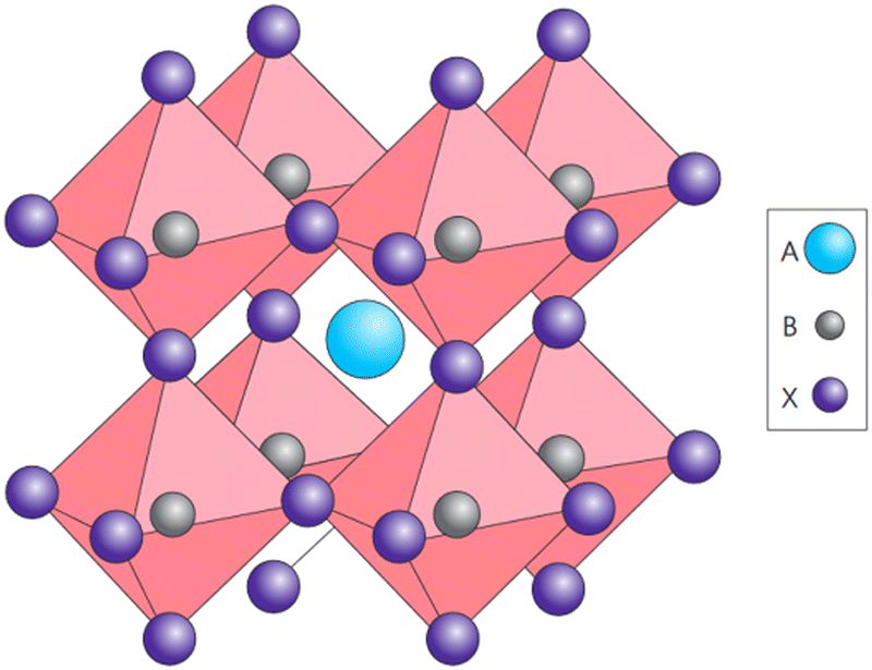 | ||
| Fig. 5 Cubic perovskite crystal structure.32 Copyright 2014, Springer Nature. | ||
Direct deposition of perovskite layers to achieve a double-layer structure is a common strategy to construct a p–n junction in PSCs. Combining a p-type perovskite and an n-type perovskite to form a p–n homojunction can generate an additional electric field and enhance the overall BEF in PSCs,27,47 which is beneficial for the extraction and transmission of charge carriers within PSCs. Since the perovskite layer is often obtained by a solution method in PSCs, it is difficult to avoid the first deposited perovskite layer being solvated by the second deposition of the perovskite layer. According to previous reports, vapor deposition can be used to solve this problem.53–55 Dänekamp et al. first prepared a perovskite–perovskite homojunction by a vacuum deposition method.47 By adjusting the relative deposition rates of MAI and PbI2, they obtained a perovskite junction containing p-type (MAI excess) and n-type (MAI defect) MAPbI3 (Fig. 6a and b). The CPD between two different types of perovskites was measured to be 250 mV (Fig. 6c and d), which indicates the obvious existence of potential change in the junction interior. The device based on two types of perovskite layers displays a high fill factor and high photovoltage, benefiting from efficient charge extraction and limited recombination in the presence of a perovskite homojunction. Furthermore, Li et al. utilized a combined deposition method to integrate a p–n homojunction into a planar structure (Fig. 6e–h).27 There is a significant potential change between the two layers of perovskite (Fig. 6i and g), which proves the formation of an internal electric field between them, resulting in an increase in the BEF of PSCs. The BEF in the homojunction induces the directional transport of photogenerated carriers, thereby reducing the carrier recombination loss.
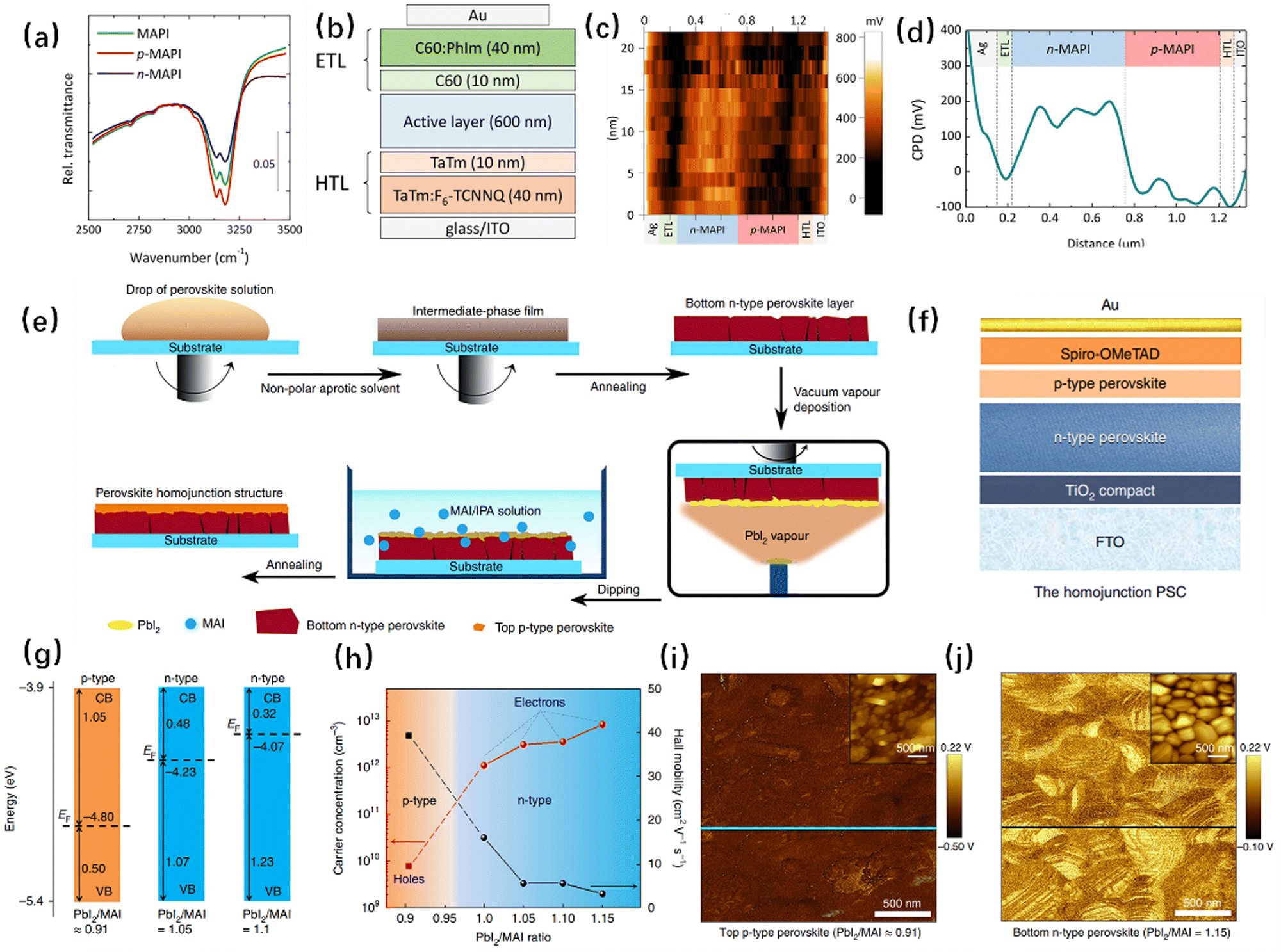 | ||
| Fig. 6 (a) IR relative transmittance spectra of the N–H stretching vibration for reference, n-type, and p-type MAPI films. (b) Scheme of the solar cell layout. (c) SKPM image of the cross section for a homojunction solar cell. (d) CPD profile of a p–n junction solar cell.47 Copyright 2018, American Chemical Society. (e) The bottom n-type perovskite layer is deposited by a one-step spin-coating method. The top p-type perovskite layer is deposited by vacuum vapour deposition followed by a dipping process. (f) The PSC with the homojunction composed by p-type and n-type perovskite layers. (g) and (h) surface potential maps (KPFM) of MAPbI3 films. (i) The energetic levels of the corresponding n-type (blue) and p-type (orange) perovskite films. (j) The carrier concentration (red symbols) and mobility (black symbols) for electrons (circle) and holes (square) in the perovskite films extracted by Hall measurements.27 Copyright 2019, Springer Nature. | ||
As for the low-dimension perovskite quantum dot films, the upper perovskite solvent does not technically dissolve the lower perovskite.56–59 During the preparation process, perovskite quantum dots are suspended in a colloidal solution through their surface ligands, and a layer of quantum dots is first deposited from the colloidal solution. The ligand is chemically removed and the resulting film is insoluble in a non-polar solvent. Thus, the subsequent quantum dot layer can be processed without affecting the lower layer film. Therefore, a perovskite double-layer structure can be prepared by quantum dot film deposition to construct a heterojunction and enhance the BEF. For example, Zhao et al. constructed an internal heterojunction by layer-by-layer deposition of perovskite quantum dots (Fig. 7a–c), which promoted charge extraction at the interface and improved photocarrier harvesting (Fig. 7d and e).59 Moreover, Li et al. prepared perovskite quantum dot solar cells with a double-layer structure (Fig. 7f).60 The combination of wide-bandgap α-CsPbI3 and narrow-bandgap FAPbI3 resulted in the formation of a heterojunction, which ensures more effective charge separation and extraction (Fig. 7g). The perovskite quantum dot deposition method provides a simple strategy for the preparation of double-layer perovskite PSCs, which is beneficial for the regulation of the BEF.
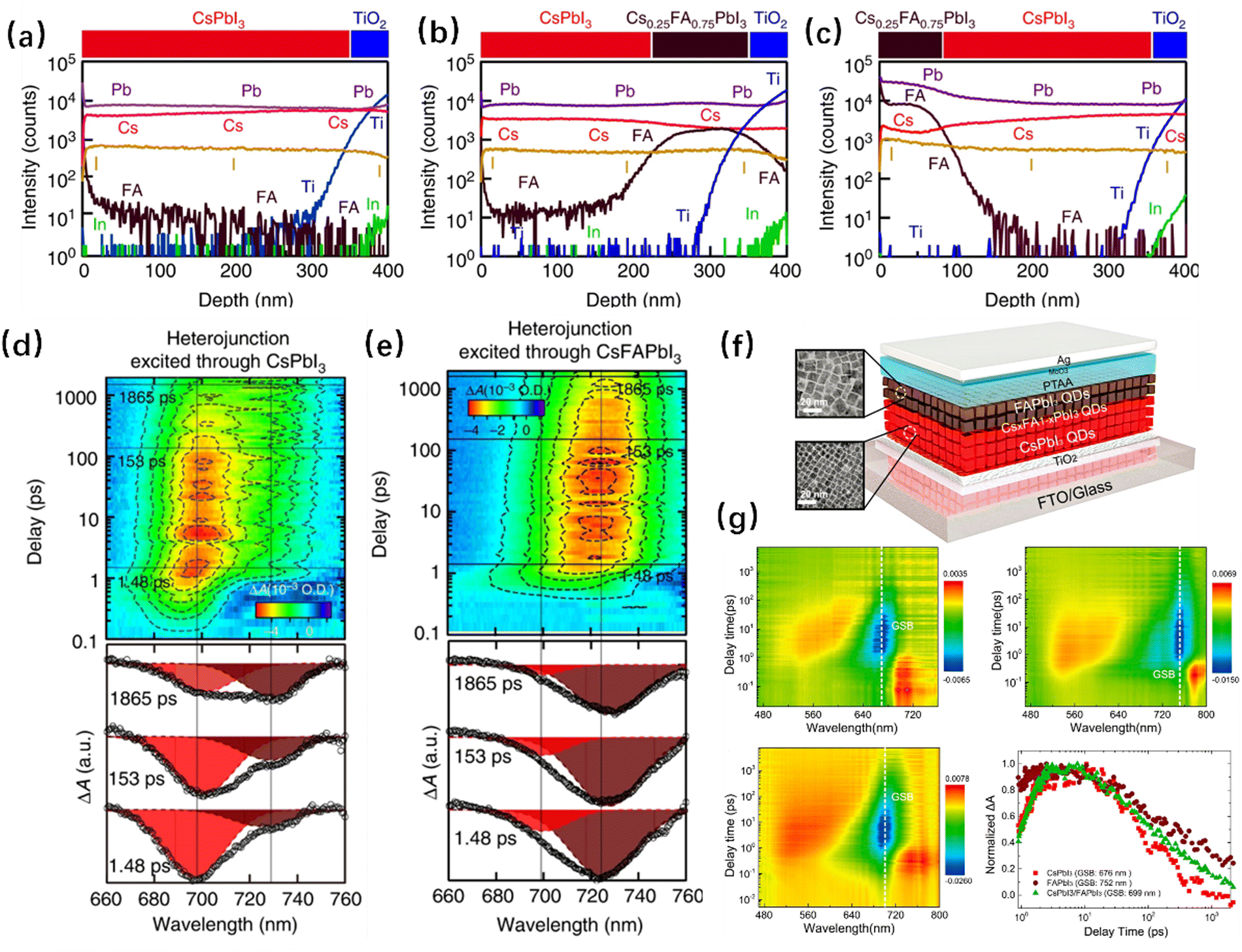 | ||
| Fig. 7 (a)–(c) ToF–SIMS depth profile of samples with the structure and interface location. (d) and (e) Transient absorption of heterojunction QD films.59 Copyright 2019, Springer Nature. (f) Schematic illustration of the PSCs. (g) TA measurements for time-wavelength-dependent TA color maps and TA spectra at a different GSB as a function of delay time.60 Copyright 2019, American Chemical Society. | ||
The construction of 2D/3D heterojunctions in PSCs is also an efficient strategy to introduce an extra electric field for efficient charge extraction. As for 2D perovskite materials, the Goldsmith tolerance factor has relatively loose restrictions on organic cations. Therefore, 2D perovskite materials are usually achieved by combining large-sized organic cations, which broadens the band gap of 2D perovskite materials. The wide bandgap of the 2D perovskite determines its weak optical performance potential and is difficult to be used as a main light absorbing material. However, this structure makes the 2D perovskite have excellent humidity stability, so it has broad application prospects in PSCs.61–66 In the past few years, many high-performance PSCs have used two-dimensional (2D) or quasi-two-dimensional (quasi-2D) perovskites modified three-dimensional (3D) perovskites to construct 2D/3D perovskite heterojunction structures. This structure can effectively enhance the BEF and achieve defect passivation and effective band alignment. Therefore, the optical performance parameters and PCE of PSCs can be improved.
Many strategies have been reported for enhancing the BEF based on 2D/3D heterojunction structures. Grancini et al. innovatively constructed the ultra-stable 2D/3D (HOOC(CH2)4NH3)2PbI4/CH3NH3PbI3 perovskite junction of carbon-based structure.67 This work prepared a stable 2D/3D heterojunction in PSCs and improved the stability of PSCs. He et al. applied dodecyl ammonium bromide (DABr) to react with PbI2 in GBs, which formed a clear 2D/3D heterojunction and increased the intensity of the BEF (Fig. 8a).68 At the same time, the super-long chain organic molecules have a good hydrophobic effect, which can inhibit the penetration of water and effectively improve the humidity stability (Fig. 8b and c). Furthermore, Zhou et al. developed a novel amino-functionalized fullerene (C60) derivative added to the MAPbI3 perovskite as a spacer for a 2D/3D hybrid perovskite.69 The derivative of C60 increases the electron density in the 2D/3D heterojunction and induces additional BEF enhancement (Fig. 8d), which promotes electron transport in 2D/3D PSCs. In addition, the formation of a 2D/3D heterojunction effectively reduces the trap-state density (Fig. 8e and f), which is beneficial to avoid BEF loss.
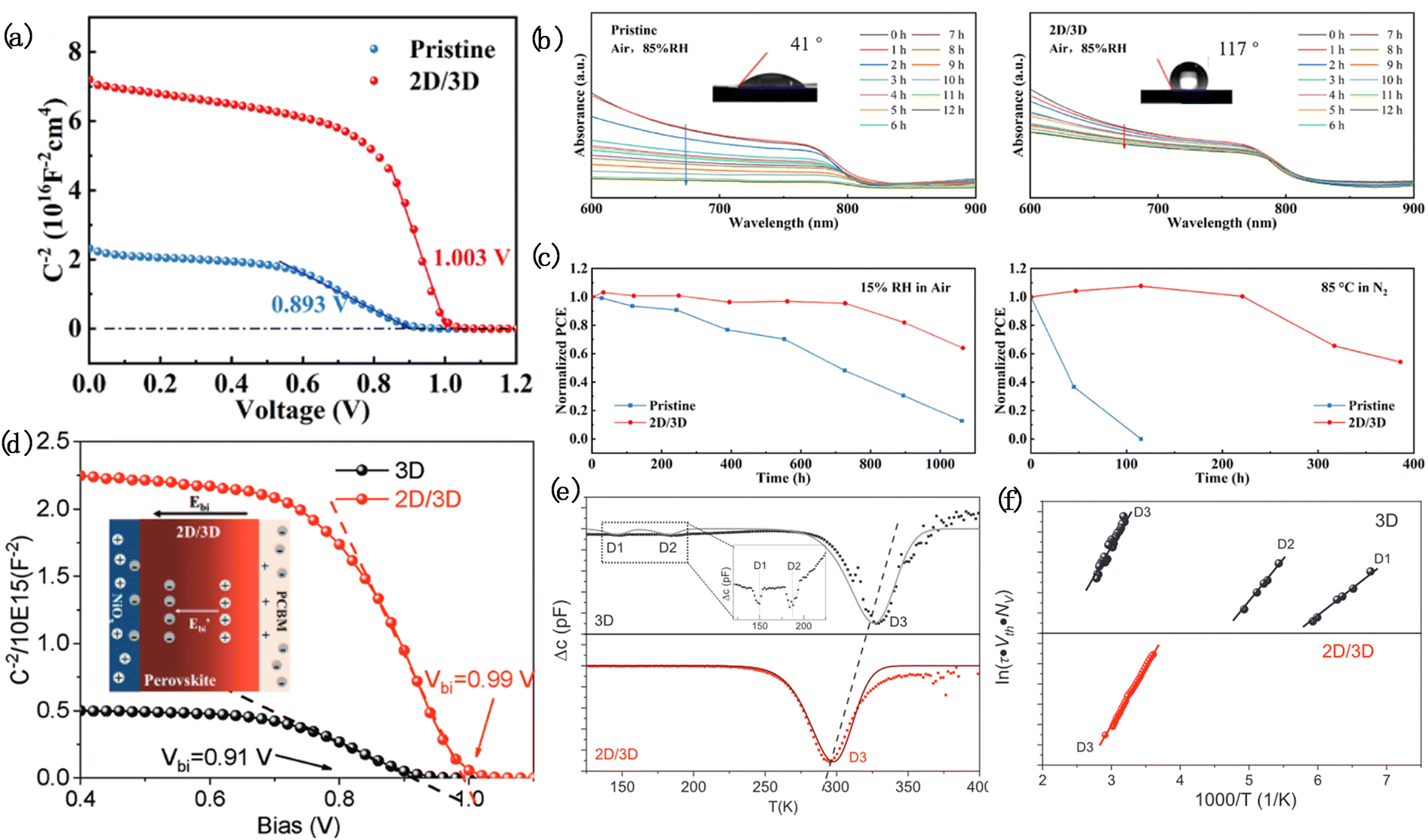 | ||
| Fig. 8 (a) Mott–Schottky plots of the pristine and 2D/3D devices. (b) Pristine and 2D/3D perovskite films exposed to ambient air with a relative humidity of 85%. Inset: contact angle images. (c) Normalized PCE of PSCs under wet conditions.68 Copyright 2022, Elsevier. (d) Schematic illustration of the BEF of the 2D/3D PSCs (inset) and Mott–Schottky curves. (e) DLTS spectra of 3D and 2D/3D PSCs. (f) Arrhenius plots obtained from DLTS signals.69 Copyright 2022, Wiley. | ||
The space charge region formed by the 2D/3D heterojunction can control the intensity of the BEF by adjusting the thickness of the 2D perovskite layer. However, the 2D perovskite obtained by the solution spin coating method will produce an additional metastable quasi-2D perovskite phase, which cannot effectively control the thickness.70 Jang et al. developed a solvent-free solid phase in plane growth (SIG) to deposit the 2D perovskite on a 3D perovskite, thus obtaining a stable and highly crystalline 2D (C4H9NH3)2PbI4 film (Fig. 9a) in PSCs and made the BEF can be designed through adjusting the width of the depletion region.71 The SIG-processed film consistently shows only one sharp peak that corresponds to a pure 2D perovskite with no formation of the quasi-2D perovskite phase (Fig. 9b), which implies that the 2D film can be grown on the 3D surface in any desired thickness by repetition of the SIG process. Finally, the BEF enhancement of PSCs (Fig. 9c) based on the 2D/3D heterojunction improves the separation and extraction of carriers. As a result, the device performance is improved, resulting in a VOC of 1.185 V and a certified steady-state efficiency of 24.35% (Fig. 9d). In this work, the thickness of the 2D perovskite layer can be approximated to the thickness of the space charge region according to the Anderson model,61 so the SIG method can directly control the BEF.
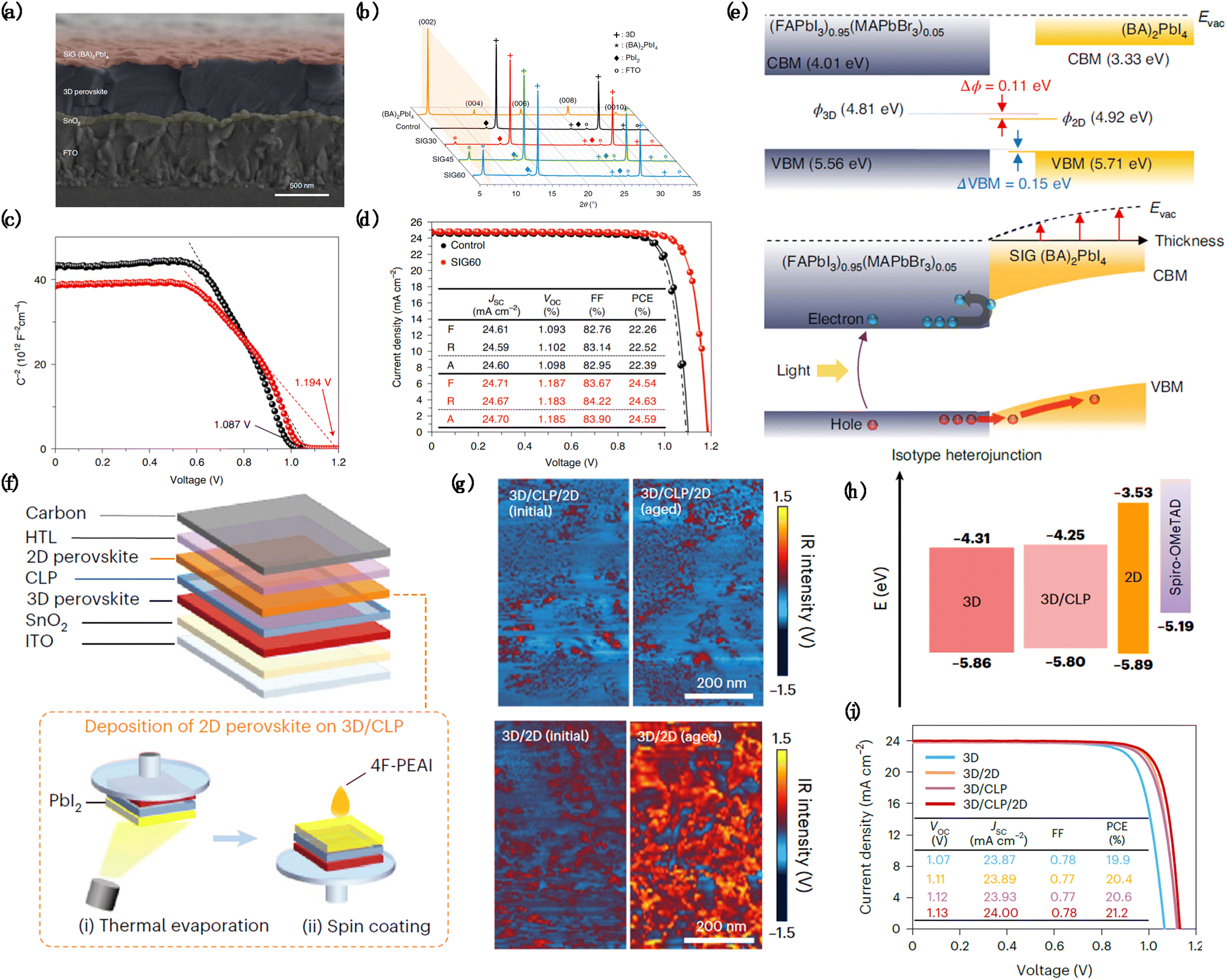 | ||
| Fig. 9 (a) X-ray diffraction patterns of the control film (3D perovskite only), 2D/3D films developed by the SIG process under different temperature conditions, and a pure 2D perovskite film. (b) A cross-sectional SEM image of the SIG-processed 2D/3D device. (c) J–V curves of 3D/2D heterojunction PSCs prepared by the SIG method. (d) Motts–Schottky plots of PSCs prepared by the SIG method. (e) Estimated energy-level alignment in the 2D/3D heterojunction. (f) Schematic diagram of the 3D/CLP/2D perovskite device structure.71 Copyright 2021, Springer Nature. (g) AFM–IR images of 3D/2D and 3D/CLP/2D perovskite heterostructures before and after aging at 100 °C for 120 min. (h) Energy diagram of the 3D perovskite, 3D/CLP, 2D perovskite and spiro-OMeTAD. (i) Representative J–V curves of PSCs fabricated using 3D perovskite, 3D/2D, 3D/CLP, and 3D/CLP/2D perovskite heterostructures as the light absorbing layer.72 Copyright 2023, Springer Nature. | ||
Furthermore, the contact between the 2D and 3D layers will result in ion diffusion, leading to the gradual disappearance of the 2D layer. To ensure the stability of the 2D/3D structure, Luo et al. introduced cross-linked polymers (CLP) into the upper layer of the 3D perovskite layer, and then deposited the 2D perovskite layer through a vapor-assisted two-step method, forming a 3D/CLP/2D perovskite heterostructure (Fig. 9e and f). The CLP stabilizes the heterostructure by inhibiting the diffusion of cations between 2D and 3D perovskites (Fig. 9g). Meanwhile, the introduction of the CLP can optimize the energy level alignment (Fig. 9h). In this work, PSCs based on carbon electrodes achieved an efficiency of 21.2% (Fig. 9i).72
It is a challenge to construct gradient heterojunctions with precise controllable and ideal energy level distribution for enhancing the BEF and realizing high-performance PSCs.76 Various strategies have been reported to achieve high-quality gradient heterojunctions for PSCs. For example, Li et al. realized energy level gradient distribution by regulating the halogen ratio of CsPbX3 and formed a gradient heterojunction with MAPbI3 to prepare a hole-free device (Fig. 10a).77 The increase in the proportion of bromides will broaden the energy band and increase the valence band maximum (VBM) of the perovskite, which can expand the difference between the Fermi levels of the acceptor and the donor in the gradient heterostructure. Therefore, the multi-layer distribution meeting the gradient energy level orientation can be prepared (Fig. 10b). The existence of the gradient heterojunction enhances the BEF and provides an additional hole driving force, which is beneficial for the separation of electron–hole pairs in the perovskite light absorption layer.
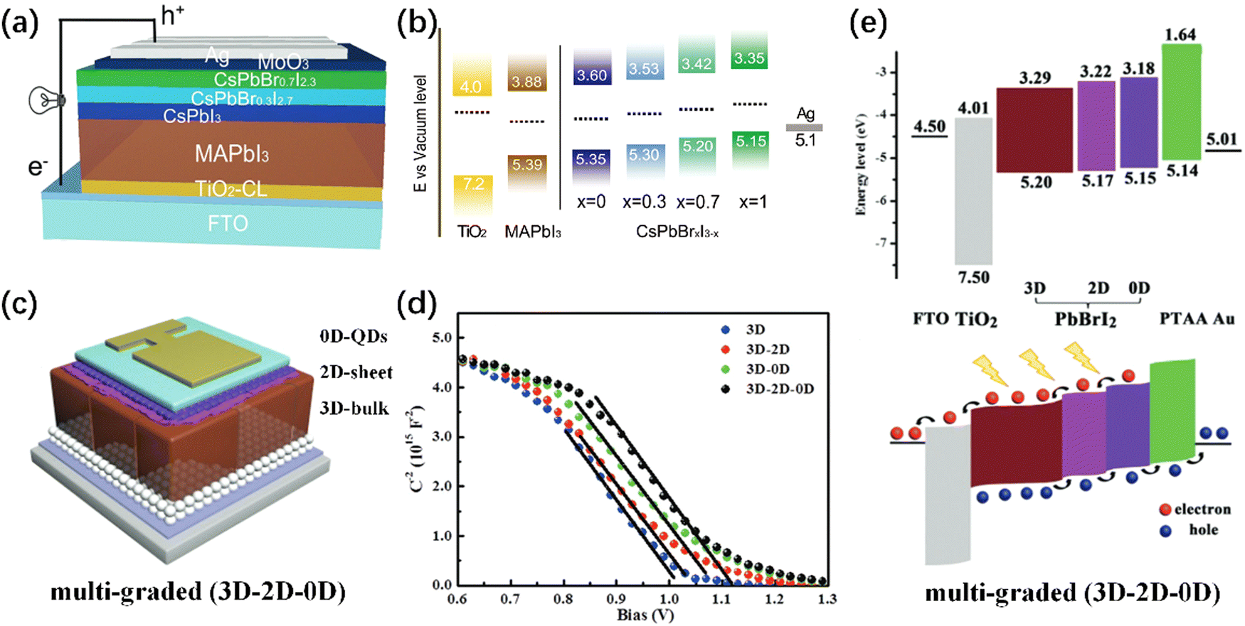 | ||
| Fig. 10 (a) Schematic diagram of solar cell configuration with graded CsPbBrxI3−x films. (b) Energy diagram of solar cells with graded CsPbBrxI3−x.77 Copyright 2017, Wiley. (c) Schematic diagram of the gradient structure of the 3D–2D–0D perovskite. (d) Mott–Schottky curves with/without dimensional gradient heterojunctions. (e) Energy-level diagram of multigrade CsPbBrI2 PSCs (top) and the carrier-transport mechanism in multigrade CsPbBrI2 PSCs (bottom).78 Copyright 2018, Wiley. | ||
Furthermore, gradient heterojunctions can be designed by low-dimensional perovskites. Zhang et al. prepared inorganic perovskite material CsPbBrI2 into bulk–nanosheet–quantum dots (3D–2D–0D) dimensional structures to obtain a multiple dimensional gradient heterojunction (Fig. 10c).78 The introduction of the 3D–2D–0D gradient junction optimized the energy level orientation (Fig. 10e) and enhanced the BEF of the PSC device (Fig. 10d). Zhu et al. introduced different Ln3+ (Yb3+, Ce3+, Eu3+, and Sm3+) doped CsPbBrCl2 perovskite quantum dots (PQDs) to prepare high-performance PSCs.79 In this work, Ln3+ was doped in CsPbBrCl2 PQDs and applied to PSCs to achieve gradient doping of Ln3+. The introduction of Ln3+ formed a stronger Ln–I bond than Pb–I, which can adjust the WF, optimize the band alignment, and thus enhance the BEF (Fig. 11a–c). In addition, the CsPbBrCl2:Sm3+ modified PSCs have the optimal band alignment that can reduce interface carrier recombination. The PSC device based on the MAPbI3 modified with CsPbBrCl2:Sm3+ showed a maximum PCE of 22.52% and a high VOC of 1.20 V, representing 91% of the S–Q limit. In addition, the strategy of constructing gradient heterojunctions to enhance the BEF is of great significance for the preparation of lead-free environment-friendly PSCs. Wu et al. prepared a FASnI3 perovskite layer with a vertical Sn2+ gradient (Fig. 11d–f) to construct a heterostructure. In this work, the Fermi level moves up from the bottom to the top with the increase of Sn2+ content, which generates an additional electric field, and thus enhances the BEF and minimizes the bulk recombination loss inside the tin perovskite.80
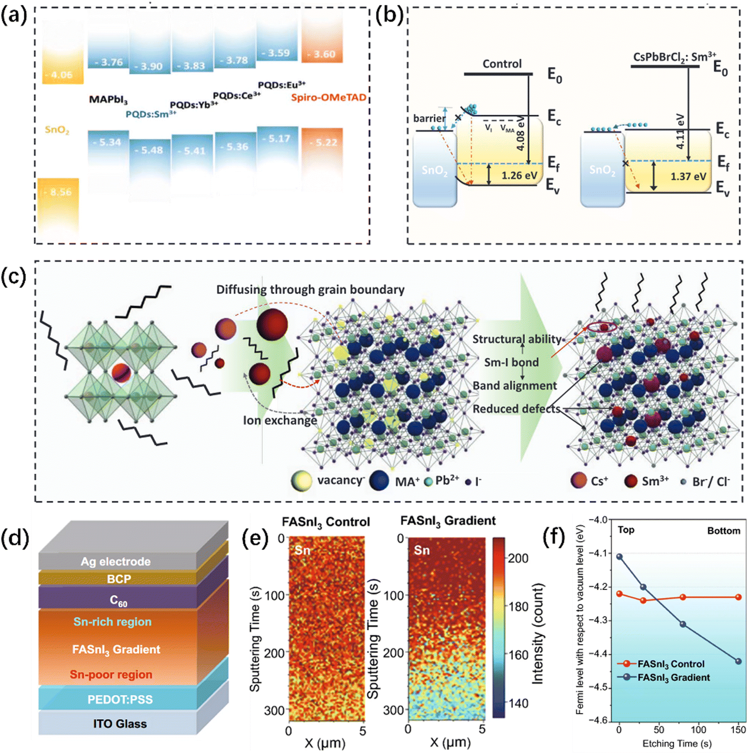 | ||
| Fig. 11 (a) Bandgap alignment for layers in a PSC device. (b) Schematic diagrams of energy band alignment for control and CsPbBrCl2:Sm3+ devices. (c) Schematic of the MAPbI3 perovskite crystal with defects and schematic of the proposed CsPbBrCl2:Sm3+ modified perovskite crystal structure.79 Copyright 2022, Wiley. (d) Schematic illustration of the gradient FASnI3-based inverted PSCs. (e) TOF–SIMS 2D mapping profiles of Sn along the x–z plane for the FASnI3 control and FASnI3 gradient films. (f) Depth profiles of the Fermi level in FASnI3 control and FASnI3 gradient films derived from the valence-band XPS analysis.80 Copyright 2022, Springer Nature. | ||
Meanwhile, the design of heterojunctions is not limited to the perovskite layer. Wu et al. hetero-epitaxially grew rutile type TiO2 single crystal array films on the fluorine-doped tin oxide (FTO) layer to construct an efficient electron selective layer with gradient Sn-doped interface by the hydrothermal method and subsequent thermal treatment.81 The Sn4+ diffuses from the FTO layer to the TiO2 film, resulting in gradient distribution of Sn4+ dopants in the film. The gradient doping induced a BEF perpendicular to the FTO substrate, which promotes the collection of photoelectrons in the TiO2 film and thus leads to the overall improvement of device performance and stability. Tan et al. obtained an interface gradient heterojunction BTA+–CsPbI3−xBrx by low-temperature treatment of quaternary bromide (BTABr) in inorganic CsPbI3 PSCs.82 The Br− in BTABr diffused into CsPbI3 thin films, which passivate coordination deficient Pb2+ and inhibit the formation of Pb clusters, effectively reducing the generation of I vacancies and suppressing non-radiative recombination. Meanwhile, the gradient Br− distribution and organic cation surface termination help to optimize the energy level arrangement between the CsPbI3 perovskite and HTL through I/Br ion exchange, thereby further promoting charge transfer in the device.
3.1.3.1. Perovskite layers. For PSCs with an inverted p–i–n structure, the perovskite layer deposited on the anode with high WF usually has a p-type surface, leading to a large degree of energy level mismatch with the ETL, which is not conducive to charge transport.83 The conversion of p-type to n-type on the perovskite surface can achieve a well-matched energy level between the perovskite layer and the ETL.84,85 Meanwhile, the p–n junction will be spontaneously formed inside the perovskite active layer to enhance the BEF. Such a strategy is also universal for PSCs with n–i–p structure.
The introduction of additives can realize the transformation of semiconductor properties in the upper layer of the perovskite, forming a similar-double-layer structure, which is classified as the p–n junction. Xiong et al. directly observed the complete transformation from p-type to n-type surface energetics of perovskite MAPbI3 in the process of defect passivation by using capsaicin as an additive.28 This leads to the spontaneous formation of a p–n homojunction located at about 100 nm below the perovskite surface (Fig. 12a–d). The presence of the p–n homogeneous junction in devices enhances the built-in potential, resulting in a high VOC of the device. Finally, an efficiency of 21.88%, a filling factor (FF) of 83.81%, and excellent device stability were achieved. Furthermore, Liu et al. adopted a double-layer modification strategy to modify the perovskite layer and the ETL by introducing different functionalized natural vitamins.86 Vitamin D2 is introduced into the perovskite layer to transform its surface energetics from n-type to p-type, forming a spontaneous n–p homojunction (Fig. 12e and f), which increases the BEF and the hole extraction efficiency of PSCs. Meanwhile, vitamin C with high conductivity is introduced into the SnO2 ETL, which improves the electron mobility of SnO2 films and reduces interface energy level offset. Therefore, the interface charge transfer ability is improved.
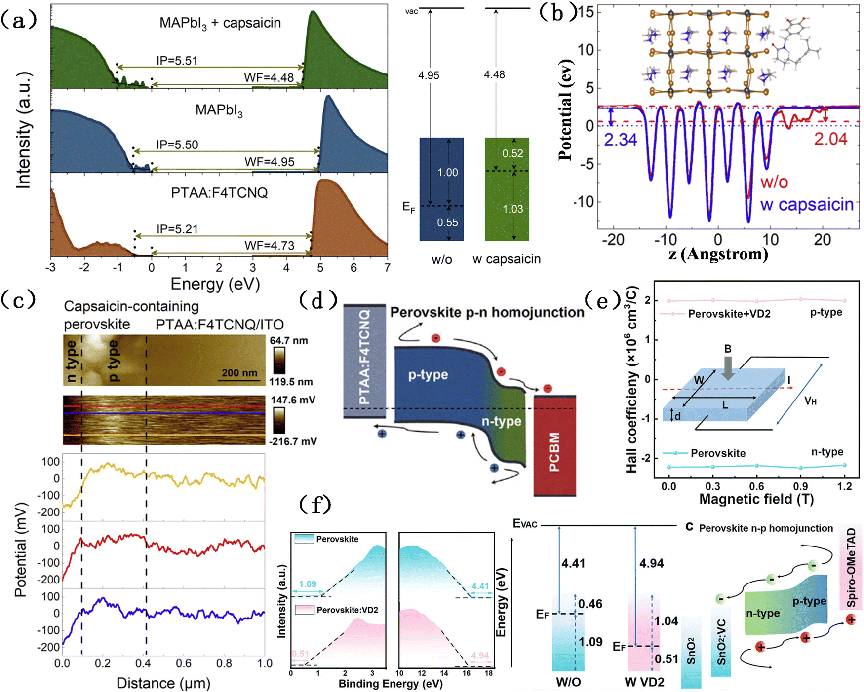 | ||
| Fig. 12 (a) UPS spectra of the secondary electron cutoff region and valence band region. (b) Calculated electrostatic potential and Fermi level of the perovskite surface with and without capsaicin. (c) Cross-sectional AFM topographies, corresponding KPFM images, and potential profiles under zero-voltage bias. (d) Energy level alignment schematics of the PSC comprising capsaicin.28 Copyright 2021, Elsevier. (e) Hall effect measurement of perovskite films. The inset shows the Hall effect measurement setup. (f) UPS spectra and energy level alignment schematics.86 Copyright 2023, Wiley. | ||
Direct cation doping can also form a p–n junction across the perovskite. Yu et al. constructed a p–n homojunction in the Sn–Pb perovskite layer by a gradient doping of Ba2+.87 The suitable Ba2+ doping can effectively compensate for p-type doping of the Sn–Pb perovskite and transform it into n-type without a change of bandgap. Induced by the unique film formation process, the distribution of Ba2+ cations is heterogeneous in perovskite films. Most of the Ba2+ remains in the top 600 nm region of the perovskite film, which turns this region into a weak n-type. In contrast, the bottom of the film remains as p-type (Fig. 13a–c). Therefore, the p–n homojunction is generated from top to bottom in the perovskite layer. The BEFs arising from this p–n homojunction facilitate the extraction of photogenerated carriers, which can increase the carrier extraction length and enhance the carrier recombination lifetime. In addition, the increased carrier extraction length offsets the negative impact of the increase in the thickness of the Sn-Pb perovskite layer. Such optimization makes Sn-Pb perovskites more suitable as a narrow band gap part of the perovskite tandem solar cells (Fig. 13d and e). Ultimately, the Sn–Pb single junction PSCs and all-perovskite tandem solar cells achieved a PCE of 21.8% and 25.3% (5.9 mm2), respectively. Moreover, doping directly at the interface can also form a junction. Li et al. prepared a heterojunction by the method of surface vulcanization to construct inverted PSCs (Fig. 13f).88 The Pb–S bond formed by surface vulcanization can shift the Fermi energy level of the perovskite interface upward. The surface energy band bending can align the energy levels of the perovskite/ETL and form a back electric field to accelerate the extraction of electrons (Fig. 13g). Finally, the resultant inverted device exhibited a PCE of 24.3% and a high VOC of 1.19 V (Fig. 13h), corresponding to a low voltage loss of 0.36 V.
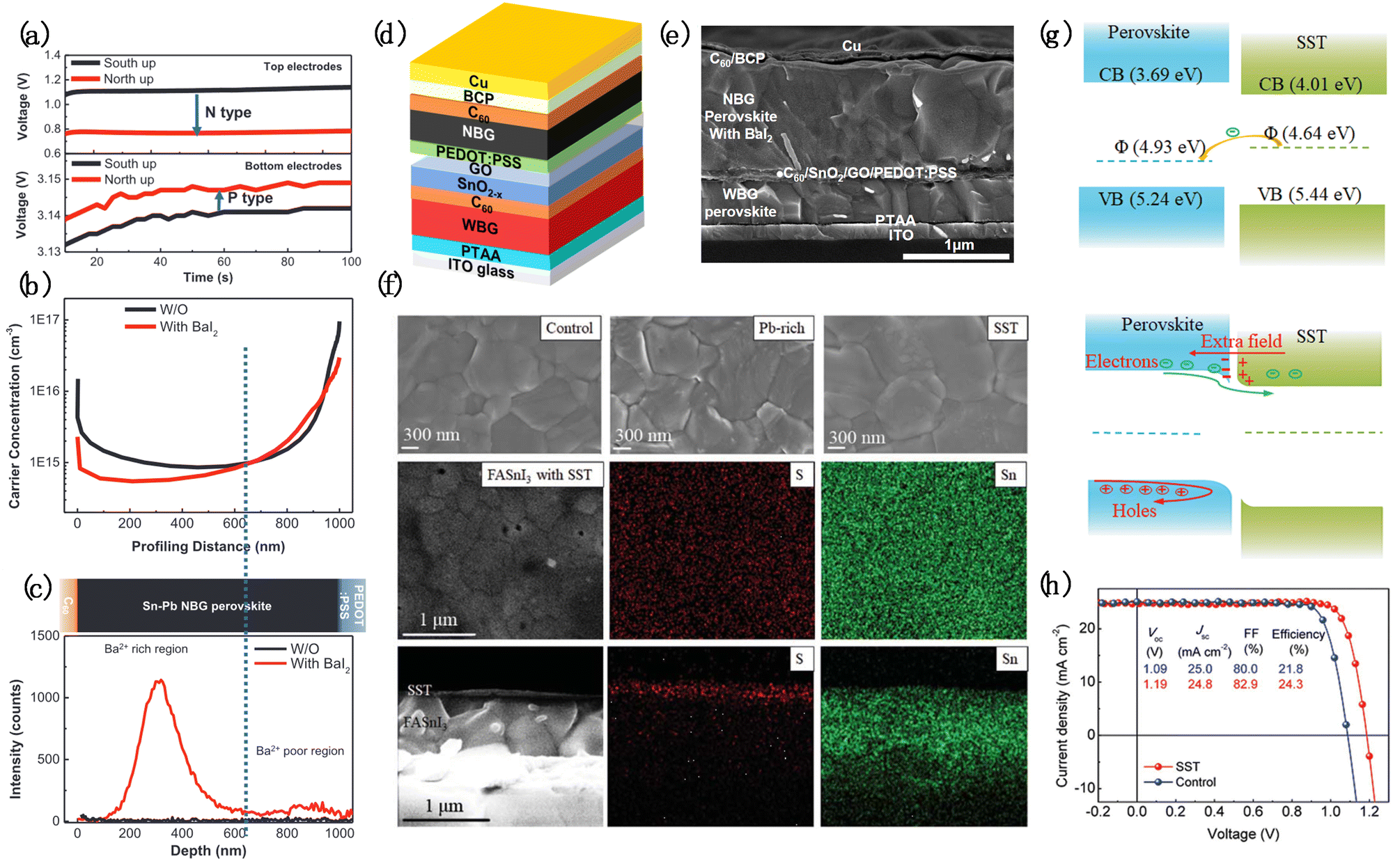 | ||
| Fig. 13 (a) Time-dependent Hall voltages for the Sn–Pb perovskite. (b) and (c) DLCP and TOF–SIMS measurements. (d) Schematic diagram of the structure. (e) Cross-sectional scanning electron microscope (SEM) image.87 Copyright 2022, Wiley. (f) SEM images, SEM–EDX mapping of the perovskite film and cross-sectional SEM–EDX mapping. (g) Energy level of perovskite films and back-surface field formation at the perovskite surface with SST. (h) J–V curves of control and SST-based PSCs.88 Copyright 2022, AAAS. | ||
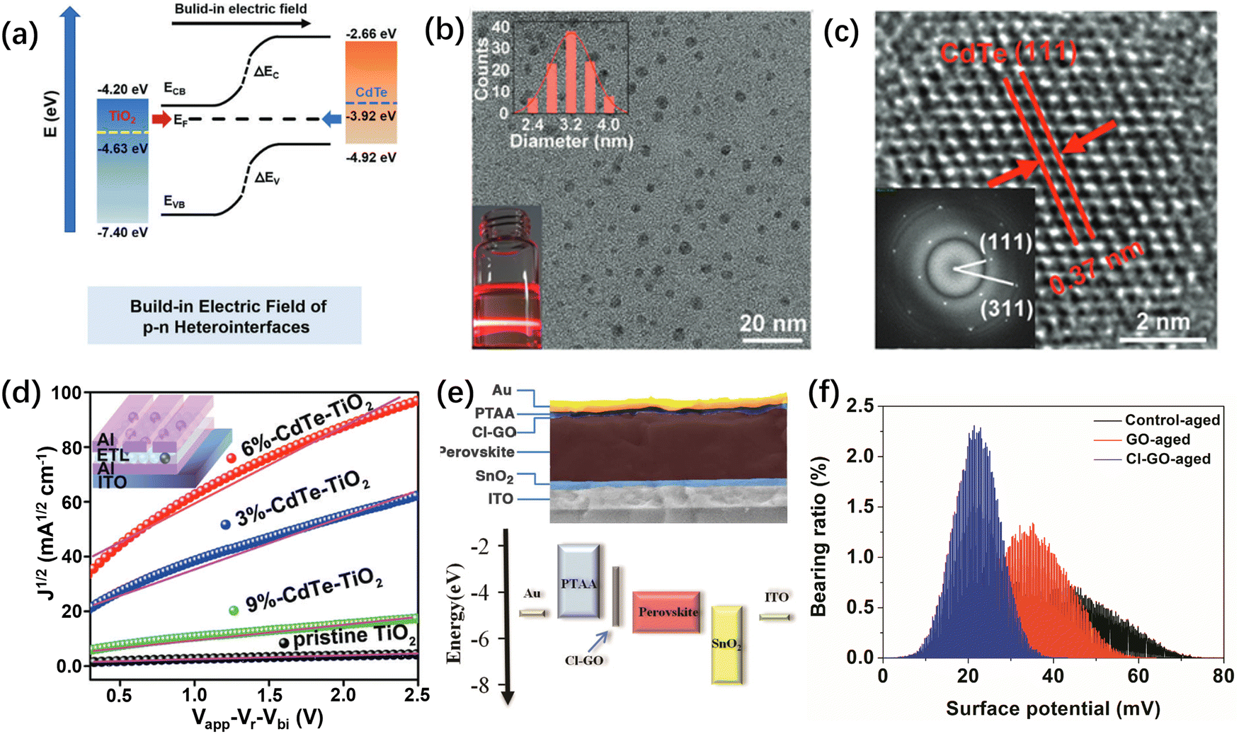
3.1.3.2. Transport layers. The commonly used transport layer usually suffers from unsatisfactory carrier mobility and mismatched interface energy level, which result in unnecessary energy loss. Introducing additional junctions in the transport layer can be used to address this issue to a certain extent. Guo et al. prepared Nb-doped SnO2 as an ETL by high target utilization sputtering (HiTUS) technology.89 The doped SnO2 ETL has a higher electron density and formed a unilateral p–n heterojunction with the perovskite layer. The p–n heterojunction can tune the built-in space-charge field in PSCs and contribute to effective carrier separation. Zhao et al. embedded a p–n heterojunction in the ETL by laser irradiation (Fig. 14a).90 The p-type CdTe NCs with Mie-scattering characteristics were prepared (Fig. 14b and c) in the precursor solvent used for the chemical bath deposition of the TiO2 ETL, and then positioned at the particle boundary of the TiO2 ETL by liquid phase pulsed laser irradiation technology. The formation of the p–n heterogeneous interface in the CdTe-TiO2 electron transport layer produces numerous localized BEFs, which improves the transport of photogenerated carriers and increases the electron mobility (Fig. 14d).
 | ||
| Fig. 14 (a) Schematic illustration of the functions of embedded p–n heterointerfaces. (b) TEM image of CdTe NCs (inset: size distribution diagram and Mie-scattering image). (c) HRTEM and corresponding fast Fourier transform of CdTe NCs. (d) Electron mobilities of different ETLs using the SCLC model.90 Copyright 2023, Wiley. (e) Cross-sectional SEM image of the cell and the schematic energy level alignment of the cell. (f) The distribution of surface potential measured by KPFM.91 Copyright 2019, AAAS. | ||
3.1.3.3. Introducing an intermediate layer. The heterostructure of the perovskite layer and the transport layer is crucial for the extraction of photogenerated carriers. In general, on the perovskite side of the heterostructure, the component elements are fixed by relatively weak chemical bonds, such as ionic bonds, hydrogen bonds, and van der Waals interactions. The weak bonding property makes the soft lattice of the perovskite easy to decompose, so it is difficult to form stable heterostructures in the perovskite. It has been reported that the unbonded ions in the perovskite may diffuse to the transport layer, destroy the heterojunction, and thus weaken the BEF. The stability of the heterojunction is affected by light, heat, electric field, and other factors.91–94 The introduction of a suitable intermediate layer can enhance the stability of the junction and can form a new junction. Wang et al. reported a stable heterojunction structure prepared by a solution method.91 By introducing chlorinated graphite oxide (Cl-GO) as the intermediate layer (Fig. 14e) between the lead-rich perovskite surface and poly-triarylamines (PTAA), the interaction of Cl-GO and the perovskite layer forms strong Pb–Cl and Pb–O bonds. The constructed stable heterostructure (Fig. 14f) can reduce charge recombination and efficiently extract photogenerated charge carriers. Furthermore, Hu et al. studied the formation of the MAPbI3/graphene heterojunction by graphene-coating through first-principles calculations.95 This structure can resist the instability of the perovskite caused by a humid environment and enhance the BEF.
3.2. Regulating the energy level
The energy level alignment between contacting semiconductors plays a critical role in improving the performance of PSCs due to its great impact on the separation and recombination of photogenerated charge carriers. In general, the energy level mismatch in PSCs would lead to severe non-radiative recombination and low charge extraction efficiency.96–99 Selecting the appropriate functional layer is considered to be an important strategy for forming well-matched energy levels to reduce interfacial carrier recombination and enhance charge extraction. The CB (VB) of the HTL (ETL) should be chosen to provide the energy barrier for selective electron (hole) extraction, which can be achieved through high bandgap materials. The unobvious potential barrier can lead to unexpected accumulation of charge carriers, resulting in the reverse electric field, leading to enhanced recombination of charge carriers.100,101 In contrast, the VB/CB of the HTL (ETL) should be aligned with the VB/CB of perovskite absorbers to allow for effective majority charge extraction.99As is well known, the difference in the WF between two contacts strongly influences the formation of a BEF in PSCs, in which the WF arises from the difference between the vacuum level and the Fermi level.15 Thus, the regulation of the energy level for selective contact layers can be used to increase the BEF for maximizing charge extraction and VOC. The excellent energy level orientation between functional layers would effectively avoid the loss of the BEF. At the same time, on the premise of energy level alignment, expanding the WF difference between the two poles/transport layers can enhance the BEF.102 Tuning the energy level position of selective contact layers, including the ETL/HTL and perovskite layer, can optimize the WF difference in PSCs. The Fermi level of the selective contact materials can be tuned via vacancy defect doping, substitution doping, and molecule modification. In this chapter, we divide the strategy of energy level regulation into the construction of a dipole layer and functional layer modification. The former is a kind of interface engineering, which can efficiently and directly adjust the WF of the perovskite surface to achieve the enhancement of the BEF. The latter changes the WF by developing and modifying the HTL and the ETL.
Lee et al. applied p-doped poly(9,9-bis(4′-sulfonatobutyl)fluorene-alt-co-1,4-(2,5-dimethoxy)phenylene) (p-PFP-O) as a HTL for the anode and poly[(9,9-bis(3′-(N,N-dimethylamino)propyl)-2,7-fluorene)-alt-2,7(9,9-dioctylfluorene)] (PFN) as an ETL for the cathode (Fig. 15a and b).29 The introduction of this strong electric dipole expands the WF difference of the interface between the electrode and the transport layer, thus enhancing the BEF in PSCs. Wang et al. introduced electric dipole molecules PTFCN and CF3BACl to enhance the WF difference Δμ1 between the two electrodes and Δμ2 between the upper and lower surfaces of the perovskite (Fig. 15c).107 Ultimately, the maximization of the BEF can be achieved within the controllable range. Yu et al. developed Ni phthalocyanine (NiPc) modified by four methoxy group ethoxy units as hole transporting materials (HTMs).108 The molecular structure of NiPc effectively increases the intramolecular dipole, which builds an intramolecular electric field inside NiPc and accelerates charge transport. Ansari et al. applied quasi-3D aziridine lead iodide (AzPbI3) as the surface intermediate layer of the primary 3D perovskite film. The existence of AzPbI3 dipoles on the surface of the perovskite changes the WF, which provides an enhanced electric field and thus improves the photovoltaic parameters significantly.109
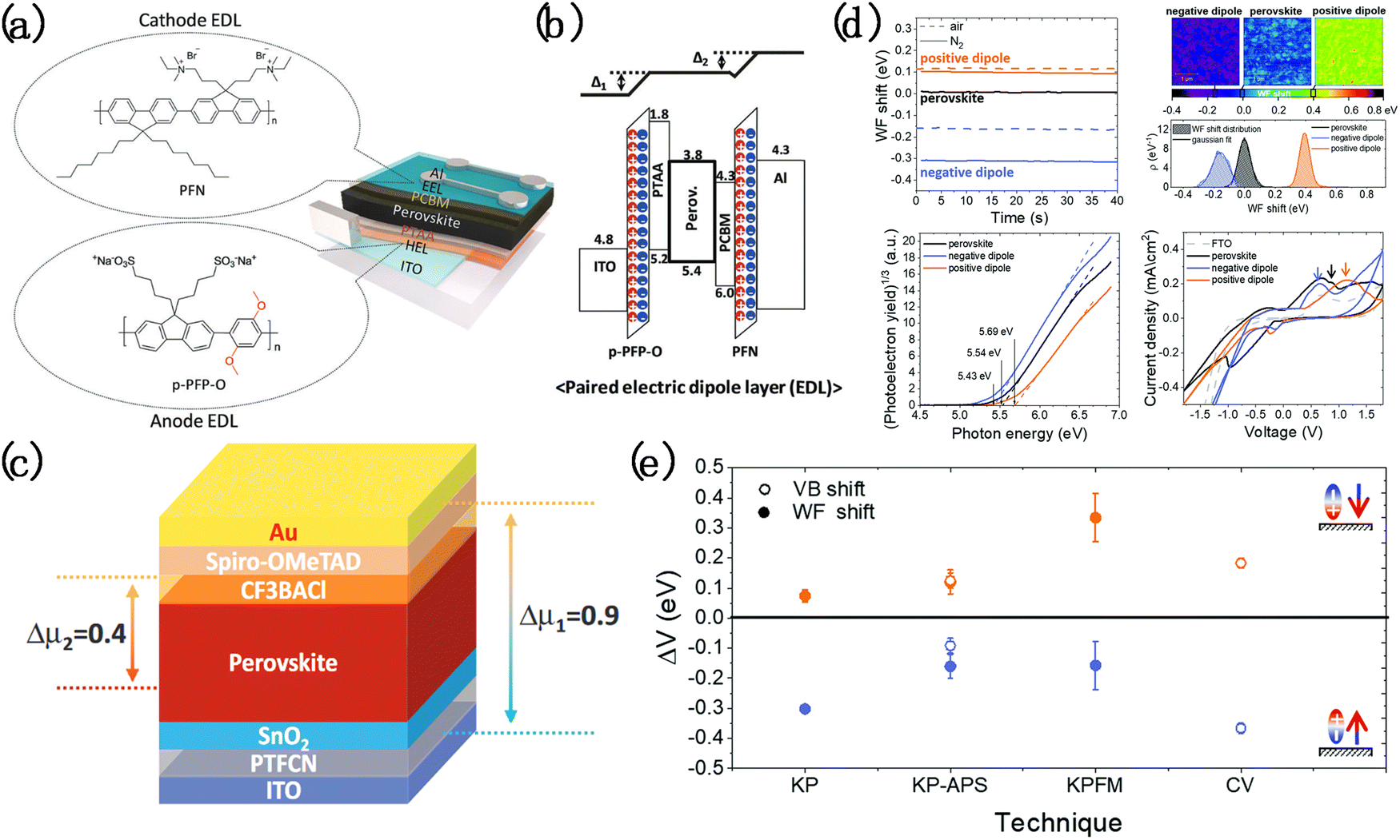 | ||
| Fig. 15 (a) Chemical structures of EDL materials and schematic device architecture, and (b) corresponding energy level diagrams.29 Copyright 2018, RSC. (c) Structure of a PSC device.15 Copyright 2020, Wiley. (d) WF shift measured with a Kelvin probe (KP), Kelvin probe force microscopy (KPFM), ambient pressure photoelectron spectroscopy (APS) and cyclic voltammetry (CV); the order is upper left, upper right, lower left and lower right. (e) Comparison of the WF shift and VB shift related to the perovskite obtained with different techniques for the cases of a positive and negative dipole.110 Copyright 2021, RSC. | ||
Furthermore, Canil et al. induced stable dipoles on the surface of a perovskite using self-assembled monolayers (SAM) to regulate the WF of the perovskite.110 The “positive dipole” and “negative dipole” are defined in this work. The former is the case where the total dipole points to the perovskite surface, and the latter is the opposite. The perfluorodecyl iodide as a positive dipole will cause an upshift of the vacuum energy level, resulting in an increase in the WF of the functionalized material, and the effect of amyl sulfide as a negative dipole is the opposite. Meanwhile, a strategy that combines multiple characterization methods was proposed to ensure the measurement accuracy of the WF (Fig. 15d and e), which is beneficial for directly selecting the molecular type and deposition conditions to adjust the WF of the perovskite and then designing a controllable energy level structure to regulate the BEF. In addition, Liu et al. used organic–inorganic (OI) complexes (CL-CH3 and CL-CF3) as multifunctional interlayers to prepare high-performance PSCs by a two-step continuous method.111 The introduction of the intermediate layer not only passivates the defects of the perovskite film but also forms a vertical dipole moment, which enhances the BEF and facilitates the extraction of charge carriers.
For example, Kamarudin et al. replaced formamidinium iodide (FAI) with dimethylammonium iodide (DMAI) partly, which is a strategy of A-site cation substitution to improve the performance of lead-free (Sn-based) PSCs.112 The oxidation of Sn2+ is inhibited due to DMAI doping, resulting in a decrease of defect density and hole (p-type) carrier density. Finally, the beneficial effect of DMAI is demonstrated by BEF enhancement and VOC improvement. Moreover, Zhang et al. doped LiI into MAPbI3 to modulate the interface energy band alignment and facilitate the carrier transport.113 The non-intrinsic Li+ and I− were introduced as ion dopants in MAPbI3, which significantly improved the ionic conductivity in the perovskite (Fig. 16a). Meanwhile since both Li+ and I− can move within the perovskite structure, there is excessive I− aggregation at the Ag anode, and the Li+ is considered to concentrate on the FTO side due to its high mobility group (Fig. 16b). The aggregation of Li+/I− regulated the energy levels of the perovskite and induced n/p doping in MAPbI3. Li+ shifts the Fermi energy level upward to form n-type doping and I− causes the Fermi energy level to move down, thereby achieving p doping (Fig. 16c). Finally, the doping of LiI optimizes the energy level orientation of tin-based PSCs and enhances the BEF.
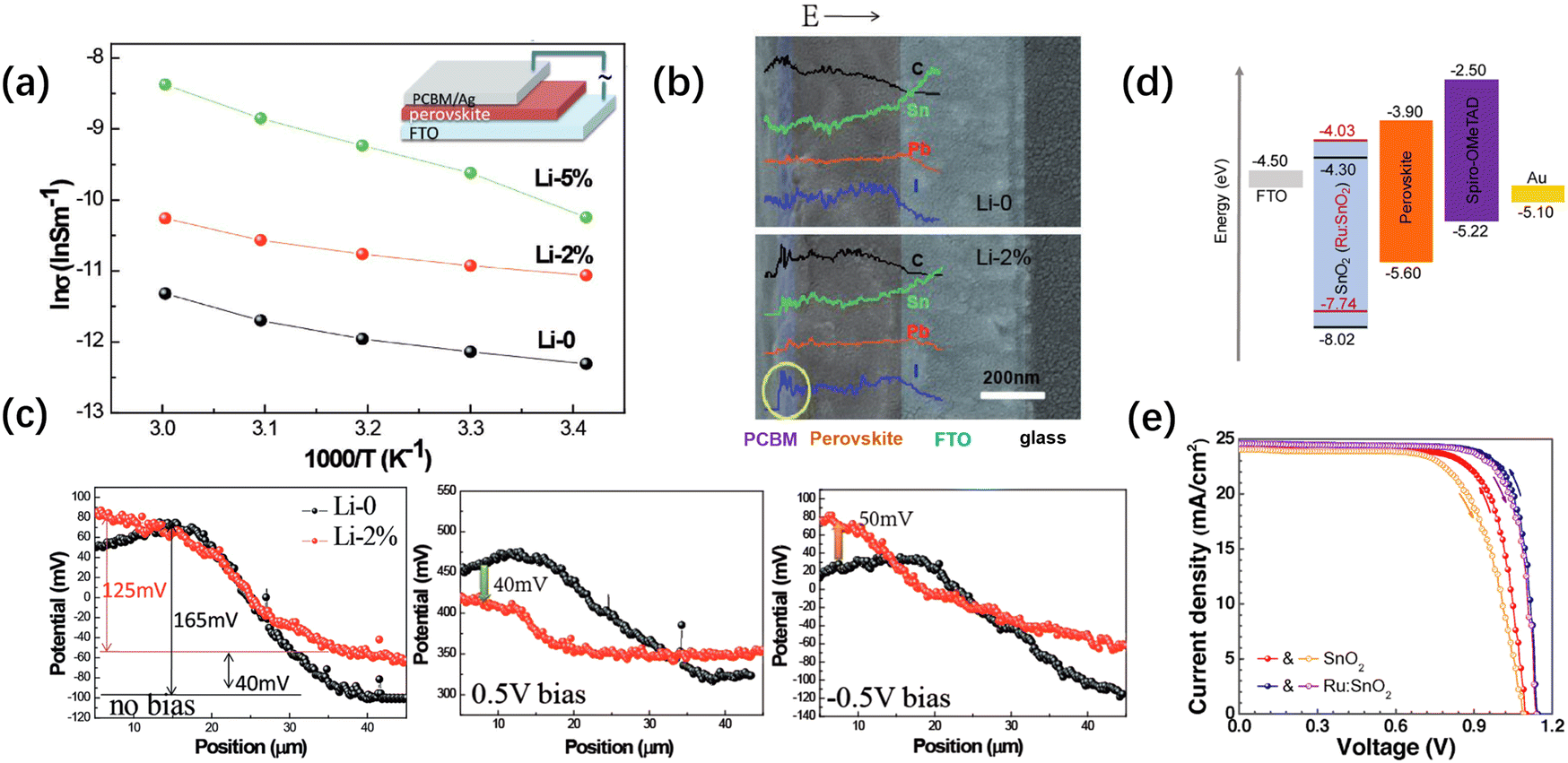 | ||
| Fig. 16 (a) EDX linear scan of the element distribution. (b) σ–T plots of Li-0, 2, and 5% in Arrhenius coordinates; the inset is the device structure. (c) The surface potential profiles (line scan) at 0 V bias, 0.5 V bias, and −0.5 V bias.113 Copyright 2017, Wiley. (d) Schematic illustration of the energy level diagram of the presented PSCs. (e) Hysteresis curves.114 Copyright 2019, ACS. | ||
In addition to perovskite layers, the electrode and transport layers can be modified by additive doping to enhance energy level matching. Furthermore, other influencing factors, such as hole/electron mobility and electrical conductivity, are usually considered to achieve the best performance. Zhou et al. regulated the WF of the TiO2 ETL and ITO electrodes to improve interface contact by modifying them with Y-doping and polyethylenimine ethoxylate (PEIE), respectively.115 After regulating, the ITO/PEIE electrode and the Y-TiO2 ETL achieve energy level alignment, which is conducive to efficient transport of electrons between the ETL and ITO layers. Xiong et al. introduced Mg into the SnO2 ETL by high-temperature treatment to change its optical properties and adjust its energy level.116 Appropriate Mg doping improves the interface contact, reduces the free electron density, and increases the electron mobility, which increases the electron driving force and thus facilitates the electron transfer at the ETL/perovskite interface. Wang et al. doped Ru into the TiO2 ETL to improve the performance and conductivity of PSCs.117 Ru doping significantly reduced the electron trap density of the ETL, which avoids excessive charge accumulation and ensures effective electron injection at the ETL/perovskite interface. Akin used Ru-doped SnO2 as the ETL to improve the photoelectric properties of PSCs.114 The incorporation of Ru makes the Fermi level of the SnO2 ETL move up (Fig. 16d), which improves the energy level alignment of the ETL/perovskite interface and thus enhances the BEF of the device and improves VOC and electron extraction. In addition, the device prepared by this work has almost no hysteresis (Fig. 16e).
Furthermore, Liu et al. doped p-type dopant 2,3,5,6-tetrafluoro-7,7,8,8-tetracyanoquinodimethane (F4-TCNQ) into the HTL to improve the photovoltaic performance of inverted PSCs.118 The low concentration of F4-TCNQ doping can effectively adjust the electrical properties of PEDOT:PSS films and reduce the highest occupied molecular orbital (HOMO) energy level. Therefore, the enhanced conductivity and optimized energy level arrangement of doped thin films allow for effective carrier transport from the perovskite absorption layer to the HTL. Seo et al. used Zn-TFSI2 to replace Li-TFSI2 as a p-type dopant for HTL material spiro-MeOTAD in PSCs.119 Therefore, the hole mobility was increased by an order of magnitude and the BEF was significantly enhanced. Jiang et al. developed a Spiro-OMeTAD layer modified with MoS2, which plays an important role in improving the hole mobility of Spiro-OMeTAD and enhancing the stability of the film.120
3.3. Constructing a ferroelectricity polarized electric field
The ferroelectricity PEF has been widely studied. When the polarization of the ferroelectric phase causes the dipole to be oriented in a specific direction, a PEF is generated. In some reports, it is also called the ferroelectric built-in electric field (FBEF).121 The generation of the PEF enhances the intensity of the BEF in PSCs, which helps to separate and extract charge carriers, thereby realizing a high-performance PSC device.122,123 Understanding the concept of ferroelectricity is of great significance for studying the PEF of the ferroelectric phase. The ferroelectric crystal has both thermoelectric and piezoelectric properties (Fig. 17a), and the polarization direction can be switched according to the direction of the external electric field (EEF). This characteristic of reorienting the spontaneous polarization direction under external bias can lead to polarization hysteresis, which manifests as a polarization-electric field hysteresis loop (P–E loop). The P–E loop is a macroscopic description of the change of the ferroelectric domain under the action of an EEF, which can reflect the ferroelectric properties of materials (Fig. 17b). In addition, the temperature boundary between the paraelectric phase and the ferroelectric phase of ferroelectric materials is called the Curie temperature (Tc). The crystals below Tc will show ferroelectricity. Determining the value of Tc can demonstrate whether the ferroelectric material can exhibit ferroelectricity at room temperature.124,125 Therefore, the P–E loop and Tc can be used to prove the existence of ferroelectricity. In this chapter, we introduce the strategies for designing a PEF by using ferroelectricity, including the application of perovskite ferroelectricity and the doping of ferroelectric materials.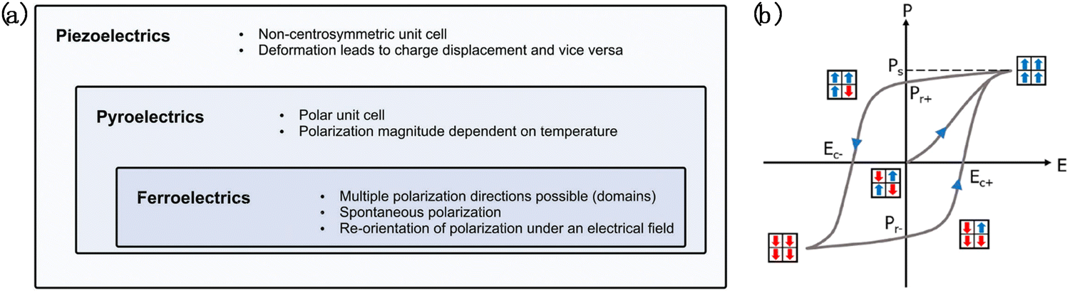 | ||
| Fig. 17 (a) Diagram of the non-centrosymmetric crystal classes and their ferroic properties.121 Copyright 2019, Wiley. (b) Schematic illustration of the hysteresis loop for electric displacement versus electric field.126 Copyright 2023, ACS. | ||
In order to apply the PEF to halide perovskite photovoltaics, the ferroelectricity of halide perovskites has been studied recently, including the transformation of the ferroelectric crystal phase, the existence of ferroelectric domains in the perovskite and the mechanism of the switchable photovoltaic effect. Walsh et al. established a computational model to study the lattice polarization affected by polar organic cations and verified the existence of spontaneous polarization in the MAPbI3 perovskite.131 The ferroelectric domains in the perovskite will lead to internal junctions, which is beneficial for the separation of e–h pairs and reduction of recombination. By using piezoelectric response force microscopy (PFM), Röhm et al. demonstrated that MAPbI3 possesses alternating polarization domains with a width of 90 nm, which were identified as polarized ferroelectric domains (Fig. 18a).132 This work directly observed the presence of ferroelectric domains in perovskites. Rossi et al. modeled different polarization configurations based on the alternating ferroelectric domain patterns measured by PFM (Fig. 18b). The polarization model was combined with drift–diffusion simulations to study the influence of ferroelectric domains on charge separation and recombination losses in PSCs.122 This work proved that the presence of ordered ferroelectric domains improves the VOC by reducing the Schockley–Read–Hall (SRH) recombination loss and forms a high conductive channel to improve the carrier extraction, thereby improving the PCE.
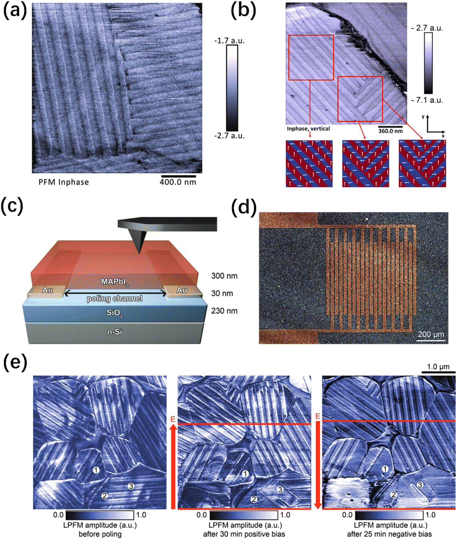 | ||
| Fig. 18 (a) High-resolution PFM.132 Copyright 2017, RSC. (b) Piezoresponse force micrograph recorded on a typical MAPbI3(Cl) grain surface and three polarization patterns.122 Copyright 2018, Elsevier. (c) Layout of the sample architecture used for poling experiments. (d) Top-view optical microscope image of the MAPbI3 layer atop interdigitated gold electrodes. (e) LPFM images before polarization, after polarization, and after subsequent reverse polarization.133 Copyright 2020, Wiley. | ||
Furthermore, Röhm et al. demonstrated that MAPbI3 films exhibited spontaneous polarization during the transition from the cubic phase (above Tc) to the tetragonal phase (below Tc).121 The polarization is mainly in-plane orientation as probed by PFM. Drift–diffusion simulation on ferroelectric domains with alternating polarization indicated that the presence of a ferroelectric built-in electric field is beneficial for reducing the SRH recombination of charge carriers in perovskite grains. Subsequently, they proved that applying an EEF can achieve ferroelectric poling of MAPbI3.133 The microscopic modulation of the polar domains under the EEF and the concurrent persistent shift of the currents indicate that MAPbI3 is a ferroelectric semiconductor. However, since MAPbI3 has higher conductivity compared to conventional insulating ceramic ferroelectrics, applying an electric field can drive remarkable current through MAPbI3, which will damage the PSC device. To avoid this situation, this work designed a sample architecture (as shown in Fig. 18c and d), allowing in-plane poling of the MAPbI3 layer. Based on this method, a mild electric field can be applied to avoid sample damage, and the change of the polarization domain in the electric field can be directly observed by lateral PFM (LPFM) (Fig. 18e). Controlling the ferroelectric polarization by the EEF is beneficial to study the ferroelectric properties of perovskites, and then regulate the intensity of the PEF.
The influence of ferroelectric polarization on the performance of PSCs was further explored. Leonhard et al. presented experimental evidence to illustrate the correlation between the ferroelectric polarization of MAPbI3 thin-films and the performance of PSCs.134 The evolution and polarization orientation of ferroelectric domains during the fabrication of MAPbI3 thin-films were investigated through PFM and KPFM. Within several seconds to minutes of the thermal annealing process, MAPbI3 thin films undergo a transition from the coexistence of out-of-plane and in-plane polarization to dominant in-plane polarization. Solar cells with alternating lateral (in-plane) domains have the best FF and efficiency, while solar cells with vertical (out-of-plane) domains only exhibit moderate performance. Moreover, solar cells with out-of-plane polarization exhibit lower stability during the process of electrical characterization. Through this work, it can be seen that the evolution of ferroelectric domains in perovskite thin films is an important factor to affect the final device performance.
The ferroelectricity of 3D perovskites is still controversial in current reports. Edmands et al. measured the conductance hysteresis of CH3NH3PbI3 perovskite thin films by a double-wave method, which excluded the hysteresis effect caused by ferroelectricity in PSCs and emphasized the importance of ion migration.135 Coll et al. demonstrated by piezoelectric force microscopy (PFM) and macroscopic polarization methods that MAPbI3 does not exhibit permanent polarization at room temperature.136 This work suggests that the transient polarization at room temperature may be related to the photogenerated dipole induced by intrinsic charge transfer. Almora et al. showed that the enhancement of capacitance observed in a capacitance–voltage experiment for MAPbI3 at a specific frequency is related to the overlap effect of the interface cumulative capacitance, and the light-induced changes in the dielectric properties of the perovskite can be ignored.137 Tong et al. demonstrated that MAPbI3 may exhibit fluctuating polar nanoregions (especially below 190 K), and it is difficult to obtain a stable ferroelectric phase.138 These reports show that the abnormal photovoltaic behavior of 3D perovskites do not necessarily originate from their own ferroelectric properties. In addition, even if 3D perovskites exhibit ferroelectricity, there are often harsh constraints, such as specific temperatures. Therefore, the ferroelectricity of 3D perovskites cannot be well applied in photovoltaic devices.
Although the ferroelectricity of 3D perovskites has limitations, the positive role of the ferroelectricity PEF in PSCs is still worth looking forward to. The 3D structure of perovskite ABX3 has strict requirements for the size of each component. Exploring perovskites towards low dimensionality (including 2D, 1D, and 0D) can broaden the tunability of perovskites.139–142 In fact, the ferroelectric design of low-dimensional perovskites has fewer constraints on the A-site organic cation, so it is easy to obtain low-dimensional ferroelectric perovskites. For example, introducing large hydrophobic organic cations to construct 2D perovskites can induce ferroelectricity of perovskites.30 However, low-dimensional perovskites usually exhibit a large band gap and are difficult to directly apply as light absorption materials in PSCs. It is an effective strategy to combine low-dimensional perovskites with traditional 3D perovskites as a light absorber.
The 2D ferroelectric perovskites are usually used to construct a 2D intermediate layer structure in PSCs. The ferroelectricity of 2D perovskites can be controlled by modulating the dipole moment. Inducing the ferroelectricity of 2D perovskites based on 2D/3D heterostructures can provide a PEF and thus effectively enhance the BEF in PSCs.143–145 Yang et al. obtained 2D PbI2 perovskite ferroelectrics for the first time by introducing chiral cations (Fig. 19a).146 As shown in Fig. 19b and c, the 180° reversal of the PFM phase signal and the typical butterfly ring of the amplitude signal demonstrate the switching ability of ferroelectric domain polarization.
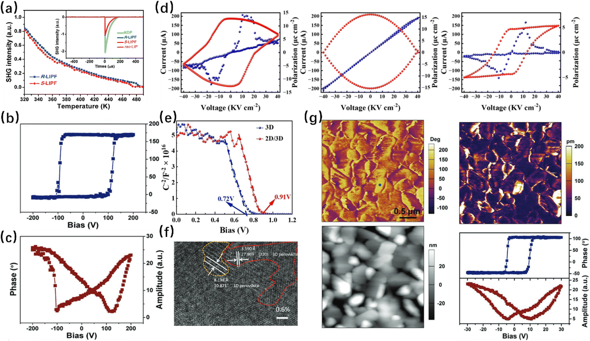 | ||
| Fig. 19 (a) Temperature dependence of the SHG intensity. (b) and (c) Vertical PFM phase and amplitude signals as functions of the tip voltage for a selected point at room temperature, showing local PFM hysteresis loops.146 Copyright 2019, Wiley. (d) I–E curve and P–E curve of 2D, 3D and 2D/3D perovskite films. (e) Mott–Schottky plots of devices.30 Copyright 2023, Wiley. (f) HRTEM image of the 0.6% molar ratio 1D/3D mixed perovskite. Scale bar: 2 nm. (g) PFM phase, amplitude images, topographic image of the thin film and dependence of phase and amplitude signals with applied DC bias for a selected point.148 Copyright 2021, Wiley. | ||
Subsequently, Chen et al. reported a 2D ferroelectric perovskite (4-aminotetrahydropyran)2PbBr4[(ATHP)2PbBr4] with a huge piezoelectric voltage coefficient (g33).147 This molecular ferroelectric has a higher Tc and its g33 is twice that of polyvinylidene fluoride (PVDF). Han et al. designed a ferroelectric 2D perovskite based on a pyridine heterocyclic ring as the organic intermediate layer.30 The P–E loop of the sample exhibits the ferroelectric polarization inversion (Fig. 19d), indicating the obtained 2D perovskite has ferroelectricity. The incorporation of ferroelectric 2D materials into 3D perovskites leads to an increase in the BEF (Fig. 19e), thereby improving the exciton dissociation efficiency in a device. Furthermore, the applications of 1D ferroelectric perovskites have been reported. Zhang et al. combined 1D ferroelectric perovskite trimethyliodomethylammonium tris(μ2-iodo)-lead with 3D perovskite (FAPbI3)0.85(MAPbBr3)0.15 to prepare 1D/3D perovskite films with ferroelectric properties (Fig. 19f and g).148 The enhancement of the BEF caused by ferroelectric polarization significantly improves the performance of the PSC.
Many strategies have been proposed to generate a PEF through ferroelectric doping. While introducing the ferroelectric materials, the synergistic effect of the interface dipole layer and molecular passivation should also be considered. Zhang et al. added polyvinylidene fluoride-trifluoroethylene polymer P(VDF-TrFE) as a ferroelectric dopant in the PSCs, thus broadening the depletion region and reducing the overlap of electron and hole wave functions.151 The thin layer of the polarized ferroelectric polymer film was inserted between the perovskite layer and the HTL to act as an interface dipole layer. The existence of an interface dipole layer leads to obvious band bending, which aligns the energy levels of adjacent functional layers and enhances the BEF to provide strong charge transfer force for carrier separation. Meanwhile, the F atom in the ferroelectric molecule can combine with the H atom to form an F–H bond, thereby fixing the perovskite phase structure. Through synergistic effects, this work obtained a PCE of 21.38% and a VOC of 1.14 V, with almost no hysteresis.
Furthermore, Chen et al. developed a high polarizability organic ferroelectric polymer, poly(vinylidene fluoride):dabcoHReO4 (PVDF:DH), to enhance the BEF of the FA0.92MA0.08PbI3 perovskite.152 The combination of PVDF and DH caused β phase transition of PVDF. β-PVDF with an all-trans diode arrangement has better ferroelectric properties and the F atoms on the surface can provide excellent hydrophobicity. PVDF:DH is polarized by the BEF to generate an additional PEF, which is permanently maintained in the direction consistent with the BEF direction of PSCs. The superposition of the electric field can more fully drive the transport and extraction of charge carriers, thereby obtaining excellent PCE.
3.4. Mitigating surface charge accumulation caused by ion migration
Owing to the low formation energy and migration activation energy of the ionic species in perovskite materials, the ions are prone to migrate toward and into an interface of adjacent contact layers.153 Ion migration will induce interfacial charge accumulation and generate an electric field opposite to the BEF direction, causing the shielding of the BEF present in the device.154,155 As a result, a reduced BEF would degrade the extraction efficiency of photogenerated charge carriers.156 Furthermore, the BEF screening caused by ion migration is considered to be an important factor in generating large hysteresis.157,158 During the voltage scanning process in current density–voltage (J–V) measurement, if ion accumulation occurs at the interface, the time delay between ion migration speed and scanning speed will cause hysteresis and affect the performance of PSCs.159 Therefore, it is particularly important to establish and investigate the mechanism model of the influence of ion migration on the BEF.For example, Li et al. investigated the mechanism that mainly leads to hysteresis in planar FTO/compact TiO2/CH3NH3PbI3−xClx/Spiro-OMeTAD/Ag perovskite solar cells, and attributed the hysteresis effect of PSCs to the interface barrier formed by the migration of iodide ions/interstitials.160 Belisle et al. established a “wiggly band” model of mobile ion field screening and hysteresis to demonstrate that the BEF screening caused by ion migration is an important factor leading to the hysteresis effect.161 Kim et al. studied the built-in equilibrium charge region at the interface that considered the equilibrium distribution of both ionic and electronic carriers.162 The schematic of concentration and conductivity profiles indicated that there is obvious ion adsorption and accumulation at the interface contact (Fig. 20a), which leads to the redistribution of charge. Liu et al. established a mechanism that uses the BEF as a key factor to explain ion migration and abnormal behavior of the device (Fig. 20b).163
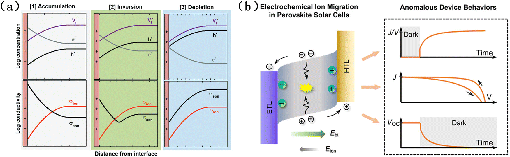 | ||
| Fig. 20 (a) Schematic concentration and conductivity profiles at the interface.162 Copyright 2022, Wiley. (b) The anomalous device behaviors caused by electrochemical ion migration.163 Copyright 2021, ACS. | ||
Based on the above research, it can be concluded that unfavorable ion migration leads to the BEF screening, which will affect the efficiency of carrier separation. To reduce the shielding of the BEF caused by ion migration, many possible strategies have been proposed in the past. Designing new functional layer materials to improve the contact at the interface and increase ion migration activation energy is an efficient strategy.164 For example, Xu et al. reported the perovskite-phenyl-C61-butyric acid methyl ester (PCBM) hybrid solid, based on which PSCs exhibited low hysteresis and recombination loss.165 Meanwhile, this work links the migration of iodide ions with the BEF and investigates the possible mechanism. Iodide anions migrate under the action of an electric field to generate ion currents. Therefore, the existence of the BEF may cause anionic charge to move in the opposite direction of the field, resulting in the decrease of photocurrent over time. PCBM can combine with iodide-rich surface sites or unincorporated iodide anions, to reduce the migration of anions through defects at grain boundaries, thus compensating the BEF.166,167 Subsequently, Zhong et al. demonstrated that PCBM could inhibit the hysteresis effect caused by ion migration and weaken the shielding effect of ion accumulation on the BEF.168 In addition, the ion compensation strategy is an effective strategy to improve interface contact. Chen et al. synthesized CuScO2 as a mesoporous HTL in inverted PSCs and pretreated the CuScO2 HTL with formamidine salt, which compensated for the iodine vacancy of the buried perovskite film.169 This ion compensation strategy can repair the ion loss in situ and reduce the charge injection barrier, thus enhancing the BEF.
The directional arrangement of dipoles in the functional layer can also improve the charge accumulation at the interface and compensate for the BEF. Ahmadi et al. studied the HTL with significant photogenerated dipoles, which can be orientationally aligned under the action of the BEF (Fig. 21a).170 The photogenerated dipole in the transport layer can trigger the charge transfer through the interface dipole field, thereby reducing the charge accumulation at the interface and BEF screening. Yang et al. inserted an effective interface dipole trimethylamine oxide (TMAO) between the perovskite layer and the ETL, which reduced the interfacial charge density and enhanced the BEF (Fig. 21b).171 In addition, the decrease of low-frequency capacitance indicates that this change of the BEF is mainly affected by the inhibition of interface charge accumulation, rather than the polarization effect of the interface dipole (Fig. 21c).172
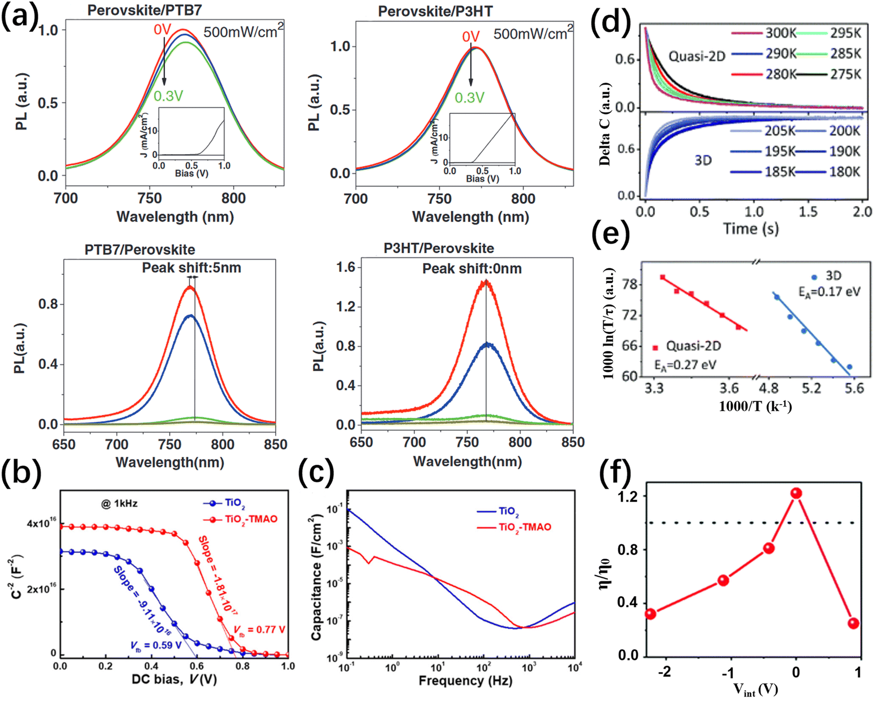 | ||
| Fig. 21 (a) Electric field-induced photoluminescence spectroscopy.170 Copyright 2017, Wiley. (b) Mott–Schottky analysis. (c) C–F plots. (d) Capacitance transients from anion migration (drift).171 Copyright 2019, ACS. (e) Arrhenius fitting results of anion migration. (f) The function of the thermal-electrical poling voltage.173 Copyright 2022, RSC. | ||
In addition to directly inhibiting ion accumulation, constructing favorable ion accumulation can induce an electric field in line with the BEF, which will improve the charge extraction efficiency and improve the device performance significantly.173,174 Such favorable ion accumulation can be achieved by using the sensitivity of ion accumulation to light, heat, and bias. For example, Lian et al. prepared high-performance quasi-2D PCSs by using light-induced favorable ion accumulation.173 Compared with the 3D perovskite, the ions in the quasi-2D perovskite have lower mobility at room temperature and higher anion activation energy (Fig. 21d and e), which excludes the influence of some unfavorable ion migration in PCSs. The light-induced quasi-Fermi level splitting compensates for the BEF. Meanwhile, the uneven ion potential caused by uneven light intensity distribution can be used to enhance favorable ion accumulation, which generates an electric field that has the same polarity as the BEF of PSCs. Furthermore, the EEF polarization can amplify the effect of beneficial ion accumulation and improve the performance of PSCs (Fig. 21f). Additionally, Xiong et al. fabricated PSCs with vertical and lateral structures and switching the direction of photocurrent by controlling the application of a small electric field (<1 V μm−1).175 This field photovoltaic effect can be explained by the formation of a reversible p–i–n structure caused by ion drift in the perovskite layer. The optimal performance parameters of the polarized single-layer vertical structure device are close to that of the optimized multi-layer device with both ETL and HTL. The introduction of the EEF can effectively guide the ion migration direction to obtain the ion accumulation polarity consistent with the BEF direction, which can enhance the BEF and improve the performance of PSCs.
4. Conclusion and outlook
The efficient extraction of photogenerated charge carriers is critical for achieving high-performance PSCs. The BEF within the PSCs can provide a driving force for carrier extraction. Various strategies have been developed to enhance the BEF to ensure efficient carrier extraction and achieve high efficiency in PSCs. In this review, the mechanism of carrier extraction affected by the BEF and the potential distribution of the BEF in PSCs are elaborated. Additionally, recent progress in the design of an enhanced BEF for efficient carrier extraction is systematically summarized. The design strategies for enhancing the BEF include constructing additional junctions based on the junction characteristics of PSCs, expanding the WF difference between the two poles in terms of the energy level, introducing the PEF from the perspective of the ferroelectric properties, and mitigating the surface charge accumulation caused by the ion migration. Through the views summarized in this review, we hope to deepen the understanding of the BEF and its effect on carrier extraction, which would help to gain an insight into the working principle of PSCs and guide further device optimization. In the last, we put forward future challenges and prospects in the design of an enhanced BEF for fabricating high-performance PSCs.(1) Constructing junctions in PSCs. The construction of junctions in PSCs, such as perovskite–perovskite junctions, gradient heterojunctions, and extra junctions, can enhance the BEF of PSCs by creating a new space charge region, leading to efficient carrier extraction. However, there are still controversies regarding the definition and characterization of these junctions in PSCs, and further research is needed to establish a conceptual model that accurately represents the structure and working principles of PSCs. Methods to directly characterize the junctions and measure the electric field intensity generated by them need to be developed. In addition, constructing heterojunctions in perovskites is an effective means to reduce carrier interface recombination through field effect passivation. Tandem solar cell devices usually suffer from serious energy loss caused by multi-interface recombination. Therefore, constructing heterojunctions in tandem solar cells is a promising research direction to reduce the energy loss and break through the S–Q limit efficiency.
(2) Energy level regulation. Regulating the energy levels in PSCs has been another approach to enhance the BEF. Strategies such as constructing dipole layers and modifying functional layers have been effective in expanding the WF difference between layers. However, accurately determining the WF shift is a challenge, as current methods like UPS require a vacuum environment, which may affect the measurement accuracy. Developing characterization techniques under atmospheric pressure, such as KPFM, APS, and CV measurements, could improve the accuracy and repeatability of energy level structure characterization. The conductivity of functional layers should also be considered when designing energy level regulation to prevent reduced carrier mobility or insulating intermediate layers.
(3) Polarized electric field in PSCs. The introduction of the ferroelectric PEF into mixed halide PSCs shows promise in improving the performance of PSCs. However, there are challenges in applying 3D ferroelectric perovskite materials, as they often exhibit a paraelectric phase and do not have the condition of spontaneous polarization at room temperature. Increasing the Tc of 3D perovskites to achieve a ferroelectric phase at room temperature by designing a new type of 3D perovskite can be a future research direction. Furthermore, optimizing the PSC device model and designing ferroelectric materials with excellent and stable characteristics can fully exploit the potential benefits of the PEF, leading to higher photovoltage and overall performance in PSCs.
(4) Mitigating surface charge accumulation caused by ion migration. Ion migration in PSCs leads to charge accumulation at the interface, which in turn causes screening of the BEF. Although several strategies have been proposed to mitigate charge accumulation and reduce BEF screening, the negative effects of ion migration in PSCs cannot be ignored. One effective strategy is doping Sn metal in Pb-based PSCs, which greatly reduces the influence of ion migration and makes it even difficult to observe in Sn-based PSCs. Therefore, B-site substituted PSCs, such as Sn-doped PSCs, can effectively reduce the influence of charge accumulation at the interface due to ion migration, resulting in PSC devices with low BEF screening.
Conflicts of interest
There are no conflicts to declare.Acknowledgements
This work was supported by the Taishan Scholars Project of Shandong Province (Grant No. 201909121) and the National Natural Science Foundation of China (22109076).References
- D. Luo, W. Yang, Z. Wang, A. Sadhanala, Q. Hu, R. Su, R. Shivanna, G. F. Trindade, J. F. Watts, Z. Xu, T. Liu, K. Chen, F. Ye, P. Wu, L. Zhao, J. Wu, Y. Tu, Y. Zhang, X. Yang, W. Zhang, R. H. Friend, Q. Gong, H. J. Snaith and R. Zhu, Enhanced photovoltage for inverted planar heterojunction perovskite solar cells, Science, 2018, 360, 1442–1446 CrossRef CAS PubMed
.
- A. Miyata, A. Mitioglu, P. Plochocka, O. Portugall, J. T.-W. Wang, S. D. Stranks, H. J. Snaith and R. J. Nicholas, Direct measurement of the exciton binding energy and effective masses for charge carriers in organic–inorganic tri-halide perovskites, Nat. Phys., 2015, 11, 582–587 Search PubMed
- Z.-K. Wang, M. Li, Y.-G. Yang, Y. Hu, H. Ma, X.-Y. Gao and L.-S. Liao, High efficiency Pb–In binary metal perovskite solar cells, Adv. Mater., 2016, 28, 6695–6703 CrossRef CAS
- H. Wei, Y. Fang, P. Mulligan, W. Chuirazzi, H.-H. Fang, C. Wang, B. R. Ecker, Y. Gao, M. A. Loi, L. Cao and J. Huang, Sensitive x-ray detectors made of methylammonium lead tribromide perovskite single crystals, Nat. Photonics, 2016, 10, 333–339 CrossRef CAS
- Z. Xiao, Y. Yuan, Q. Wang, Y. Shao, Y. Bai, Y. Deng, Q. Dong, M. Hu, C. Bi and J. Huang, Thin-film semiconductor perspective of organometal trihalide perovskite materials for high-efficiency solar cells, Mater. Sci. Eng., R, 2016, 101, 1–38 CrossRef
- J. Euvrard, Y. Yan and D. B. Mitzi, Electrical doping in halide perovskites, Nat. Rev. Mater., 2021, 6, 531–549 CrossRef CAS
- A. Kojima, K. Teshima, Y. Shirai and T. Miyasaka, Organometal halide perovskites as visible-light sensitizers for photovoltaic cells, J. Am. Chem. Soc., 2009, 131, 6050–6051 CrossRef CAS
- Best-research-cell-efficiencies, https://www.nrel.gov/pv/assets/pdfs/best-research-cell-efficiencies.pdf.
- T. R. Duncan and D. Kuhlmann-Wilsdorf, Properties of 1/2 〈110〉, {111} glide dislocations in elastically anisotropic fcc metals, Appl. Phys. Lett., 1967, 10, 105–108 CrossRef CAS
- F. Gao, Y. Zhao, X. Zhang and J. You, Recent progresses on defect passivation toward efficient perovskite solar cells, Adv. Energy Mater., 2020, 10, 1902650 CrossRef CAS
- I. Mora-Sero, L. Bertoluzzi, V. Gonzalez-Pedro, S. Gimenez, F. Fabregat-Santiago, K. W. Kemp, E. H. Sargent and J. Bisquert, Selective contacts drive carrier extraction in quantum dot solids via asymmetry in carrier transfer kinetics, Nat. Commun., 2013, 4, 2272 CrossRef
- O. J. Sandberg, J. Kurpiers, M. Stolterfoht, D. Neher, P. Meredith, S. Shoaee and A. Armin, On the question of the need for a built-in potential in perovskite solar cells, Adv. Mater. Interfaces, 2020, 7, 2000041 CrossRef CAS
- E. Siebert-Henze, V. G. Lyssenko, J. Fischer, M. Tietze, R. Brueckner, T. Menke, K. Leo and M. Riede, Electroabsorption studies of organic p–i–n solar cells: Increase of the built-in voltage by higher doping concentration in the hole transport layer, Org. Electron., 2014, 15, 563–568 CrossRef CAS
- A. Marchioro, J. Teuscher, D. Friedrich, M. Kunst, R. van de Krol, T. Moehl, M. Grätzel and J.-E. Moser, Unravelling the mechanism of photoinduced charge transfer processes in lead iodide perovskite solar cells, Nat. Photonics, 2014, 8, 250–255 CrossRef CAS
- W.-T. Wang, P. Chen, C.-H. Chiang, T.-F. Guo, C.-G. Wu and S.-P. Feng, Synergistic reinforcement of built-in electric fields for highly efficient and stable perovskite photovoltaics, Adv. Funct. Mater., 2020, 30, 1909755 CrossRef CAS
- J. Chen and N.-G. Park, Materials and methods for interface engineering toward stable and efficient perovskite solar cells, ACS Energy Lett., 2020, 5, 2742–2786 CrossRef CAS
- J. Wang, M. A. Uddin, B. Chen, X. Ying, Z. Ni, Y. Zhou, M. Li, M. Wang, Z. Yu and J. Huang, Enhancing photostability of Sn–Pb perovskite solar cells by an alkylammonium pseudo-halogen additive, Adv. Energy Mater., 2023, 13, 2204115 CrossRef CAS
- B. Li, B. Chang, L. Pan, Z. Li, L. Fu, Z. He and L. Yin, Tin-based defects and passivation strategies in tin-related perovskite solar cells, ACS Energy Lett., 2020, 5, 3752–3772 CrossRef CAS
- W. S. Yang, B.-W. Park, E. H. Jung, N. J. Jeon, Y. C. Kim, D. U. Lee, S. S. Shin, J. Seo, E. K. Kim, J. H. Noh and S. I. Seok, Iodide management in formamidinium-lead-halide-based perovskite layers for efficient solar cells, Science, 2017, 356, 1376–1379 CrossRef CAS
- Q. Jiang, Y. Zhao, X. Zhang, X. Yang, Y. Chen, Z. Chu, Q. Ye, X. Li, Z. Yin and J. You, Surface passivation of -perovskite film for efficient solar cells, Nat. Photonics, 2019, 13, 460–466 CrossRef CAS
- M. Li, H. Li, Q. Zhuang, D. He, B. Liu, C. Chen, B. Zhang, T. Pauporté, Z. Zang and J. Chen, Stabilizing perovskite precursor by synergy of functional groups for NiOx-based inverted solar cells with 23.5% efficiency, Angew. Chem., Int. Ed., 2022, 61, e202206914 CrossRef CAS PubMed
- D. Zhang, H. Zhang, H. Guo, F. Ye, S. Liu and Y. Wu, Stable α-FAPbI3 in inverted perovskite solar cells with efficiency exceeding 22% via a self-passivation strategy, Adv. Funct. Mater., 2022, 32, 2200174 CrossRef CAS
- Q. Jiang, J. Tong, Y. Xian, R. A. Kerner, S. P. Dunfield, C. Xiao, R. A. Scheidt, D. Kuciauskas, X. Wang, M. P. Hautzinger, R. Tirawat, M. C. Beard, D. P. Fenning, J. J. Berry, B. W. Larson, Y. Yan and K. Zhu, Surface reaction for efficient and stable inverted perovskite solar cells, Nature, 2022, 611, 278–283 CrossRef CAS
- T. Kumari, S. Jung, Y. Cho, H.-P. Kim, J. W. Lee, J. Oh, J. Lee, S. M. Lee, M. Jeong, J. M. Baik, W. Jo and C. Yang, A built-in electric field induced by ferroelectrics increases halogen-free organic solar cell efficiency in various device types, Nano Energy, 2020, 68, 104327 CrossRef CAS
- J. M. Ball and A. Petrozza, Defects in perovskite-halides and their effects in solar cells, Nat. Energy, 2016, 1, 16149 CrossRef CAS
- R. Sun, Q. Tian, M. Li, H. Wang, J. Chang, W. Xu, Z. Li, Y. Pan, F. Wang and T. Qin, Over 24% efficient poly(vinylidene fluoride) (PVDF)-coordinated perovskite solar cells with a photovoltage up to 1.22 V, Adv. Funct. Mater., 2023, 33, 2210071 CrossRef CAS
- P. Cui, D. Wei, J. Ji, H. Huang, E. Jia, S. Dou, T. Wang, W. Wang and M. Li, Planar p–n homojunction perovskite solar cells with efficiency exceeding 21.3%, Nat. Energy, 2019, 4, 150–159 CrossRef CAS
- S. Xiong, Z. Hou, S. Zou, X. Lu, J. Yang, T. Hao, Z. Zhou, J. Xu, Y. Zeng, W. Xiao, W. Dong, D. Li, X. Wang, Z. Hu, L. Sun, Y. Wu, X. Liu, L. Ding, Z. Sun, M. Fahlman and Q. Bao, Direct observation on p- to n-type transformation of perovskite surface region during defect passivation driving high photovoltaic efficiency, Joule, 2021, 5, 467–480 CrossRef CAS
- J.-H. Lee, J. Kim, G. Kim, D. Shin, S. Y. Jeong, J. Lee, S. Hong, J. W. Choi, C.-L. Lee, H. Kim, Y. Yi and K. Lee, Introducing paired electric dipole layers for efficient and reproducible perovskite solar cells, Energy Environ. Sci., 2018, 11, 1742–1751 RSC
- B. Han, Y. Wang, C. Liu, K. Sun, M. Yang, L. Xie, S. Yang, Y. Meng, S. Lin, P. Xu, J. Li, Q. Qiu and Z. Ge, Rational design of ferroelectric 2D perovskite for improving the efficiency of flexible perovskite solar cells over 23%, Angew. Chem., Int. Ed., 2023, 62, e202217526 CrossRef CAS
- E. Edri, S. Kirmayer, S. Mukhopadhyay, K. Gartsman, G. Hodes and D. Cahen, Elucidating the charge carrier separation and working mechanism of CH3NH3PbI3−xClx perovskite solar cells, Nat. Commun., 2014, 5, 3461 CrossRef
- M. A. Green, A. Ho-Baillie and H. J. Snaith, The emergence of perovskite solar cells, Nat. Photonics, 2014, 8, 506–514 CrossRef CAS
- I. Gur, N. A. Fromer, M. L. Geier and A. P. Alivisatos, Air-stable all-inorganic nanocrystal solar cells processed from solution, Science, 2005, 310, 462–465 CrossRef CAS
- S. D. Stranks and H. J. Snaith, Metal-halide perovskites for photovoltaic and light-emitting devices, Nat. Nanotechnol., 2015, 10, 391–402 CrossRef CAS
- J. Zhang, Y. Sun, C. Huang, B. Yu and H. Yu, Reduced open-circuit voltage loss of perovskite solar cells via forming p/p+ homojunction and interface electric field on the surfaces of perovskite film, Adv. Energy Mater., 2022, 12, 2202542 CrossRef CAS
- Y. Yuan, J. Chae, Y. Shao, Q. Wang, Z. Xiao, A. Centrone and J. Huang, Photovoltaic switching mechanism in lateral structure hybrid perovskite solar cells, Adv. Energy Mater., 2015, 5, 1500615 CrossRef
- H. Wang, H. Yu, W. Xu, Z. Yuan, Z. Yan, C. Wang, X. Liu, M. Fahlman, J.-M. Liu, X.-K. Liu and F. Gao, Efficient perovskite light-emitting diodes based on a solution-processed tin dioxide electron transport layer, J. Mater. Chem. C, 2018, 6, 6996–7002 RSC
- M. Graetzel, R. A. J. Janssen, D. B. Mitzi and E. H. Sargent, Materials interface engineering for solution-processed photovoltaics, Nature, 2012, 488, 304–312 CrossRef CAS PubMed
- Y. Zhou, L. Wang, S. Chen, S. Qin, X. Liu, J. Chen, D.-J. Xue, M. Luo, Y. Cao, Y. Cheng, E. H. Sargent and J. Tang, Thin-film Sb2Se3 photovoltaics with oriented one-dimensional ribbons and benign grain boundaries, Nat. Photonics, 2015, 9, 409–415 CrossRef CAS
- J. L. Garrett, E. M. Tennyson, M. Hu, J. Huang, J. N. Munday and M. S. Leite, Real-time nanoscale open-circuit voltage dynamics of perovskite solar cells, Nano Lett., 2017, 17, 2554–2560 CrossRef CAS PubMed
- E. Edri, S. Kirmayer, A. Henning, S. Mukhopadhyay, K. Gartsman, Y. Rosenwaks, G. Hodes and D. Cahen, Why lead methylammonium tri-iodide perovskite-based solar cells require a mesoporous electron transporting scaffold (but not necessarily a hole conductor), Nano Lett., 2014, 14, 1000–1004 CrossRef CAS PubMed
- V. W. Bergmann, S. A. L. Weber, F. Javier Ramos, M. K. Nazeeruddin, M. Grätzel, D. Li, A. L. Domanski, I. Lieberwirth, S. Ahmad and R. Berger, Real-space observation of unbalanced charge distribution inside a perovskite-sensitized solar cell, Nat. Commun., 2014, 5, 5001 CrossRef CAS PubMed
- C.-S. Jiang, M. Yang, Y. Zhou, B. To, S. U. Nanayakkara, J. M. Luther, W. Zhou, J. J. Berry, J. van de Lagemaat, N. P. Padture, K. Zhu and M. M. Al-Jassim, Carrier separation and transport in perovskite solar cells studied by nanometre-scale profiling of electrical potential, Nat. Commun., 2015, 6, 8397 CrossRef CAS PubMed
- M. Cai, N. Ishida, X. Li, X. Yang, T. Noda, Y. Wu, F. Xie, H. Naito, D. Fujita and L. Han, Control of electrical potential distribution for high-performance perovskite solar cells, Joule, 2018, 2, 296–306 CrossRef CAS
- J. Shi, J. Dong, S. Lv, Y. Xu, L. Zhu, J. Xiao, X. Xu, H. Wu, D. Li, Y. Luo and Q. Meng, Hole-conductor-free perovskite organic lead iodide heterojunction thin-film solar cells: High efficiency and junction property, Appl. Phys. Lett., 2014, 104, 063901 CrossRef
-
C. Siu, Electronic Devices, Circuits, and Applications, ed. C. Siu, Springer International Publishing, Cham, 2022, pp. 35–39 DOI:10.1007/978-3-030-80538-8_3
- B. Dänekamp, C. Müller, M. Sendner, P. P. Boix, M. Sessolo, R. Lovrincic and H. J. Bolink, Perovskite–perovskite homojunctions via compositional doping, J. Phys. Chem. Lett., 2018, 9, 2770–2775 CrossRef PubMed
- L. A. Frolova, N. N. Dremova and P. A. Troshin, The chemical origin of the p-type and n-type doping effects in the hybrid methylammonium–lead iodide (MAPbI3) perovskite solar cells, Chem. Commun., 2015, 51, 14917–14920 RSC
- Q. Wang, Y. Shao, H. Xie, L. Lyu, X. Liu, Y. Gao and J. Huang, Qualifying composition dependent p and n self-doping in CH3NH3PbI3, Appl. Phys. Lett., 2014, 105, 163508 CrossRef
- J. Kim, S.-H. Lee, J. H. Lee and K.-H. Hong, The role of intrinsic defects in methylammonium lead iodide perovskite, J. Phys. Chem. Lett., 2014, 5, 1312–1317 CrossRef CAS PubMed
- W.-J. Yin, T. Shi and Y. Yan, Unusual defect physics in CH3NH3PbI3 perovskite solar cell absorber, Appl. Phys. Lett., 2014, 104, 063903 CrossRef
- H. Li, F. Li, Z. Shen, S.-T. Han, J. Chen, C. Dong, C. Chen, Y. Zhou and M. Wang, Photoferroelectric perovskite solar cells: principles, advances and insights, Nano Today, 2021, 37, 101062 CrossRef CAS
- M. Liu, M. B. Johnston and H. J. Snaith, Efficient planar heterojunction perovskite solar cells by vapour deposition, Nature, 2013, 501, 395–398 CrossRef CAS
- L. Gil-Escrig, A. Miquel-Sempere, M. Sessolo and H. J. Bolink, Mixed iodide–bromide methylammonium lead perovskite-based diodes for light emission and photovoltaics, J. Phys. Chem. Lett., 2015, 6, 3743–3748 CrossRef CAS
- M. Sessolo, C. Momblona, L. Gil-Escrig and H. J. Bolink, Photovoltaic devices employing vacuum-deposited perovskite layers, MRS Bull., 2015, 40, 660–666 CrossRef CAS
- A. Swarnkar, A. R. Marshall, E. M. Sanehira, B. D. Chernomordik, D. T. Moore, J. A. Christians, T. Chakrabarti and J. M. Luther, Quantum dot–induced phase stabilization of α-CsPbI3 perovskite for high-efficiency photovoltaics, Science, 2016, 354, 92–95 CrossRef CAS PubMed
- E. M. Sanehira, A. R. Marshall, J. A. Christians, S. P. Harvey, P. N. Ciesielski, L. M. Wheeler, P. Schulz, L. Y. Lin, M. C. Beard and J. M. Luther, Enhanced mobility CsPbI3 quantum dot arrays for record-efficiency, high-voltage photovoltaic cells, Sci. Adv., 2017, 3, eaao4204 CrossRef PubMed
- L. M. Wheeler, E. M. Sanehira, A. R. Marshall, P. Schulz, M. Suri, N. C. Anderson, J. A. Christians, D. Nordlund, D. Sokaras, T. Kroll, S. P. Harvey, J. J. Berry, L. Y. Lin and J. M. Luther, Targeted ligand-exchange chemistry on cesium lead halide perovskite quantum dots for high-efficiency photovoltaics, J. Am. Chem. Soc., 2018, 140, 10504–10513 CrossRef CAS PubMed
- Q. Zhao, A. Hazarika, X. Chen, S. P. Harvey, B. W. Larson, G. R. Teeter, J. Liu, T. Song, C. Xiao, L. Shaw, M. Zhang, G. Li, M. C. Beard and J. M. Luther, High efficiency perovskite quantum dot solar cells with charge separating heterostructure, Nat. Commun., 2019, 10, 2842 CrossRef PubMed
- F. Li, S. Zhou, J. Yuan, C. Qin, Y. Yang, J. Shi, X. Ling, Y. Li and W. Ma, Perovskite quantum dot solar cells with 15.6% efficiency and improved stability enabled by an α-CsPbI3/FAPbI3 bilayer structure, ACS Energy Lett., 2019, 4, 2571–2578 CrossRef CAS
- L. N. Quan, M. Yuan, R. Comin, O. Voznyy, E. M. Beauregard, S. Hoogland, A. Buin, A. R. Kirmani, K. Zhao, A. Amassian, D. H. Kim and E. H. Sargent, Ligand-stabilized reduced-dimensionality perovskites, J. Am. Chem. Soc., 2016, 138, 2649–2655 CrossRef CAS
- H. Tsai, W. Nie, J.-C. Blancon, C. C. Stoumpos, R. Asadpour, B. Harutyunyan, A. J. Neukirch, R. Verduzco, J. J. Crochet, S. Tretiak, L. Pedesseau, J. Even, M. A. Alam, G. Gupta, J. Lou, P. M. Ajayan, M. J. Bedzyk, M. G. Kanatzidis and A. D. Mohite, High-efficiency two-dimensional ruddlesden–popper perovskite solar cells, Nature, 2016, 536, 312–316 CrossRef CAS PubMed
- G. Grancini and M. K. Nazeeruddin, Dimensional tailoring of hybrid perovskites for photovoltaics, Nat. Rev. Mater., 2019, 4, 4–22 CrossRef CAS
- T. Zhu and X. Gong, Low-dimensional perovskite materials and their
![[thin space (1/6-em)]](https://www.rsc.org/images/entities/char_2009.gif) optoelectronics, InfoMat, 2021, 3, 1039–1069 CrossRef CAS
optoelectronics, InfoMat, 2021, 3, 1039–1069 CrossRef CAS - R. Wang, M. Mujahid, Y. Duan, Z.-K. Wang, J. Xue and Y. Yang, A review of perovskites solar cell stability, Adv. Funct. Mater., 2019, 29, 1808843 CrossRef CAS
- X. Li, J. M. Hoffman and M. G. Kanatzidis, The 2D halide perovskite rulebook: how the spacer influences everything from the structure to optoelectronic device efficiency, Chem. Rev., 2021, 121, 2230–2291 CrossRef CAS PubMed
- G. Grancini, C. Roldán-Carmona, I. Zimmermann, E. Mosconi, X. Lee, D. Martineau, S. Narbey, F. Oswald, F. De Angelis, M. Graetzel and M. K. Nazeeruddin, One-year stable perovskite solar cells by 2D/3D interface engineering, Nat. Commun., 2017, 8, 15684 CrossRef CAS
- X. He, M. Wang, F. Cao, W. Tian and L. Li, Hydrophobic long alkyl chain organic cations induced 2D/3D heterojunction for efficient and stable perovskite solar cells, J. Mater. Sci. Technol., 2022, 124, 243–251 CrossRef CAS
- W. Zhou, L. Jia, M. Chen, X. Li, Z. Su, Y. Shang, X. Jiang, X. Gao, T. Chen, M. Wang, Z. Zhu, Y. Lu and S. Yang, An improbable amino-functionalized fullerene spacer enables 2D/3D hybrid perovskite with enhanced electron transport in solar cells, Adv. Funct. Mater., 2022, 32, 2201374 CrossRef CAS
- Y. Hu, J. Schlipf, M. Wussler, M. L. Petrus, W. Jaegermann, T. Bein, P. Müller-Buschbaum and P. Docampo, Hybrid perovskite/perovskite heterojunction solar cells, ACS Nano, 2016, 10, 5999–6007 CrossRef CAS PubMed
- Y.-W. Jang, S. Lee, K. M. Yeom, K. Jeong, K. Choi, M. Choi and J. H. Noh, Intact 2D/3D halide junction perovskite solar cells via solid-phase in-plane growth, Nat. Energy, 2021, 6, 63–71 CrossRef CAS
- L. Luo, H. Zeng, Z. Wang, M. Li, S. You, B. Chen, A. Maxwell, Q. An, L. Cui, D. Luo, J. Hu, S. Li, X. Cai, W. Li, L. Li, R. Guo, R. Huang, W. Liang, Z.-H. Lu, L. Mai, Y. Rong, E. H. Sargent and X. Li, Stabilization of 3D/2D perovskite heterostructures via inhibition of ion diffusion by cross-linked polymers for solar cells with improved performance, Nat. Energy, 2023, 8, 294–303 CrossRef CAS
- Y. Hou, X. Chen, S. Yang, C. Li, H. Zhao and H. G. Yang, A band-edge potential gradient heterostructure to enhance electron extraction efficiency of the electron transport layer in high-performance perovskite solar cells, Adv. Funct. Mater., 2017, 27, 1700878 CrossRef
- T. Wang, W. Deng, J. Cao and F. Yan, Recent progress on heterojunction engineering in perovskite solar cells, Adv. Energy Mater., 2023, 13, 2201436 CrossRef CAS
- N. Yan, Y. Gao, J. Yang, Z. Fang, J. Feng, X. Wu, T. Chen and S. Liu, Wide-bandgap perovskite solar cell using a fluoride-assisted surface gradient passivation strategy, Angew. Chem., Int. Ed., 2023, 62, e202216668 CrossRef CAS PubMed
- Z. Ning, D. Zhitomirsky, V. Adinolfi, B. Sutherland, J. Xu, O. Voznyy, P. Maraghechi, X. Lan, S. Hoogland, Y. Ren and E. H. Sargent, Graded doping for enhanced colloidal quantum dot photovoltaics, Adv. Mater., 2013, 25, 1719–1723 CrossRef CAS PubMed
- B. Li, Y. Zhang, L. Zhang and L. Yin, Graded heterojunction engineering for hole-conductor-free perovskite solar cells with high hole extraction efficiency and conductivity, Adv. Mater., 2017, 29, 1701221 CrossRef PubMed
- J. Zhang, D. Bai, Z. Jin, H. Bian, K. Wang, J. Sun, Q. Wang and S. Liu, 3D–2D–0D interface profiling for record efficiency all-inorganic CsPbBrI2 perovskite solar cells with superior stability, Adv. Energy Mater., 2018, 8, 1703246 CrossRef
- X. Zhuang, R. Sun, D. Zhou, S. Liu, Y. Wu, Z. Shi, Y. Zhang, B. Liu, C. Chen, D. Liu and H. Song, Synergistic effects of multifunctional lanthanides doped CsPbBrCl2 quantum dots for efficient and stable MAPbI3 perovskite solar cells, Adv. Funct. Mater., 2022, 32, 2110346 CrossRef CAS
- T. Wu, X. Liu, X. Luo, H. Segawa, G. Tong, Y. Zhang, L. K. Ono, Y. Qi and L. Han, Heterogeneous FASnI3 absorber with enhanced electric field for high-performance lead-free perovskite solar cells, Nano-Micro Lett., 2022, 14, 99 CrossRef CAS PubMed
- T. Wu, C. Zhen, H. Zhu, J. Wu, C. Jia, L. Wang, G. Liu, N.-G. Park and H.-M. Cheng, Gradient Sn-doped heteroepitaxial film of faceted rutile TiO2 as an electron selective layer for efficient perovskite solar cells, ACS Appl. Mater. Interfaces, 2019, 11, 19638–19646 CrossRef CAS PubMed
- S. Tan, C. Tan, Y. Cui, B. Yu, Y. Li, H. Wu, J. Shi, Y. Luo, D. Li and Q. Meng, Constructing an interfacial gradient heterostructure enables efficient CsPbI3 perovskite solar cells and printed minimodules, Adv. Mater., 2023, 35, 2301879 CrossRef CAS PubMed
- S. Olthof and K. Meerholz, Substrate-dependent electronic structure and film formation of MAPbI3 perovskites, Sci. Rep., 2017, 7, 40267 CrossRef CAS PubMed
- Y.-N. Lu, J.-X. Zhong, Y. Yu, X. Chen, C.-Y. Yao, C. Zhang, M. Yang, W. Feng, Y. Jiang, Y. Tan, L. Gong, X. Wei, Y. Zhou, L. Wang and W.-Q. Wu, Constructing an n/n+ homojunction in a monolithic perovskite film for boosting charge collection in inverted perovskite photovoltaics, Energy Environ. Sci., 2021, 14, 4048–4058 RSC
- X. Chang, J.-X. Zhong, G. Yang, Y. Tan, L. Gong, X. Ni, Y. Ji, Y. Li, G. Zhang, Y. Zheng, Y. Shao, J. Zhou, Z. Yang, L. Wang and W.-Q. Wu, Targeted passivation and optimized interfacial carrier dynamics improving the efficiency and stability of hole transport layer-free narrow-bandgap perovskite solar cells, Sci. Bull., 2023, 68, 1271–1282 CrossRef CAS PubMed
- B. Liu, Y. Wang, Y. Wu, Y. Zhang, J. Lyu, Z. Liu, S. Bian, X. Bai, L. Xu, D. Zhou, B. Dong and H. Song, Vitamin natural molecule enabled highly efficient and stable planar n–p homojunction perovskite solar cells with efficiency exceeding 24.2%, Adv. Energy Mater., 2023, 13, 2203352 CrossRef CAS
- Z. Yu, X. Chen, S. P. Harvey, Z. Ni, B. Chen, S. Chen, C. Yao, X. Xiao, S. Xu, G. Yang, Y. Yan, J. J. Berry, M. C. Beard and J. Huang, Gradient doping in Sn–Pb perovskites by barium ions for efficient single-junction and tandem solar cells, Adv. Mater., 2022, 34, 2110351 CrossRef CAS PubMed
- X. Li, W. Zhang, X. Guo, C. Lu, J. Wei and J. Fang, Constructing heterojunctions by surface sulfidation for efficient inverted perovskite solar cells, Science, 2022, 375, 434–437 CrossRef CAS PubMed
- R. Guo, Y. Zhao, Y. Zhang, Q. Deng, Y. Shen, W. Zhang and G. Shao, Significant performance enhancement of all-inorganic CsPbBr3 perovskite solar cells enabled by Nb-doped SnO2 as effective electron transport layer, Energy Environ. Mater., 2021, 4, 671–680 CrossRef CAS
- W. Zhao, P. Guo, C. Liu, N. Jia, Z. Fang, L. Ye, Q. Ye, Y. Xu, A. P. Glotov, A. A. Novikov, V. A. Vinokurov, D. Harvey, D. Shchukin and H. Wang, Laser derived electron transport layers with embedded p–n heterointerfaces enabling planar perovskite solar cells with efficiency over 25%, Adv. Mater., 2023, 35, 2300403 CrossRef CAS PubMed
- Y. Wang, T. Wu, J. Barbaud, W. Kong, D. Cui, H. Chen, X. Yang and L. Han, Stabilizing heterostructures of soft perovskite semiconductors, Science, 2019, 365, 687–691 CrossRef CAS PubMed
- A. Amat, E. Mosconi, E. Ronca, C. Quarti, P. Umari, M. K. Nazeeruddin, M. Grätzel and F. De, Angelis, Cation-induced band-gap tuning in organohalide perovskites: interplay of spin–orbit coupling and octahedra tilting, Nano Lett., 2014, 14, 3608–3616 CrossRef CAS PubMed
- C. Motta, F. El-Mellouhi, S. Kais, N. Tabet, F. Alharbi and S. Sanvito, Revealing the role of organic cations in hybrid halide perovskite CH3NH3PbI3, Nat. Commun., 2015, 6, 7026 CrossRef CAS PubMed
- Y. Zhao, W. Zhou, H. Tan, R. Fu, Q. Li, F. Lin, D. Yu, G. Walters, E. H. Sargent and Q. Zhao, Mobile-ion-induced degradation of organic hole-selective layers in perovskite solar cells, J. Phys. Chem. C, 2017, 121, 14517–14523 CrossRef CAS
- J. Hu, X. Ma, W. Duan, Z. Liu, T. Liu, H. Lv, C. Huang, L. Miao and J. Jiang, First-principles calculations of graphene-coated CH3NH3PbI3 toward stable perovskite solar cells in humid environments, ACS Appl. Nano Mater., 2020, 3, 7704–7712 CrossRef CAS
- J. Zhao, Y. Deng, H. Wei, X. Zheng, Z. Yu, Y. Shao, J. E. Shield and J. Huang, Strained hybrid perovskite thin films and their impact on the intrinsic stability of perovskite solar cells, Sci. Adv., 2017, 3, eaao5616 CrossRef PubMed
- D.-J. Xue, Y. Hou, S.-C. Liu, M. Wei, B. Chen, Z. Huang, Z. Li, B. Sun, A. H. Proppe, Y. Dong, M. I. Saidaminov, S. O. Kelley, J.-S. Hu and E. H. Sargent, Regulating strain in perovskite thin films through charge-transport layers, Nat. Commun., 2020, 11, 1514 CrossRef CAS PubMed
- X. Tang, W. Chen, D. Wu, A. Gao, G. Li, J. Sun, K. Yi, Z. Wang, G. Pang, H. Yang, R. Guo, H. Liu, H. Zhong, M. Huang, R. Chen, P. Müller-Buschbaum, X. W. Sun and K. Wang, In situ growth of all-inorganic perovskite single crystal arrays on electron transport layer, Adv. Sci., 2020, 7, 1902767 CrossRef CAS PubMed
- W. Xiang, S. Liu and W. Tress, Interfaces and interfacial layers in inorganic perovskite solar cells, Angew. Chem., Int. Ed., 2021, 60, 26440–26453 CrossRef CAS PubMed
- W. Tress and O. Inganäs, Simple experimental test to distinguish extraction and injection barriers at the electrodes of (organic) solar cells with s-shaped current–voltage characteristics, Sol. Energy
Mater. Sol. Cells, 2013, 117, 599–603 CrossRef CAS
- W. Tress, J. P. Correa Baena, M. Saliba, A. Abate and M. Graetzel, Inverted current–voltage hysteresis in mixed perovskite solar cells: polarization, energy barriers, and defect recombination, Adv. Energy Mater., 2016, 6, 1600396 CrossRef
- P. de Bruyn, A. H. P. van Rest, G. A. H. Wetzelaer, D. M. de Leeuw and P. W. M. Blom, Diffusion-limited current in organic metal-insulator-metal diodes, Phys. Rev. Lett., 2013, 111, 186801 CrossRef CAS PubMed
- B. deBoer, A. Hadipour, M. M. Mandoc, T. vanWoudenbergh and P. W. M. Blom, Tuning of metal work functions with self-assembled monolayers, Adv. Mater., 2005, 17, 621–625 CrossRef
- S. Kobayashi, T. Nishikawa, T. Takenobu, S. Mori, T. Shimoda, T. Mitani, H. Shimotani, N. Yoshimoto, S. Ogawa and Y. Iwasa, Control of carrier density by self-assembled monolayers in organic field-effect transistors, Nat. Mater., 2004, 3, 317–322 CrossRef CAS PubMed
- T. Yajima, Y. Hikita, M. Minohara, C. Bell, J. A. Mundy, L. F. Kourkoutis, D. A. Muller, H. Kumigashira, M. Oshima and H. Y. Hwang, Controlling band alignments by artificial interface dipoles at perovskite heterointerfaces, Nat. Commun., 2015, 6, 6759 CrossRef PubMed
- N. Tessler and Y. Vaynzof, Insights from device modeling of perovskite solar cells, ACS Energy Lett., 2020, 5, 1260–1270 CrossRef CAS
- J.-S. Yeo, M. Kang, Y.-S. Jung, R. Kang, S.-H. Lee, Y.-J. Heo, S.-H. Jin, D.-Y. Kim and S.-I. Na, In-depth considerations for better polyelectrolytes as interfacial materials in polymer solar cells, Nano Energy, 2016, 21, 26–38 CrossRef CAS
- Z. Yu, L. Wang, X. Mu, C.-C. Chen, Y. Wu, J. Cao and Y. Tang, Intramolecular electric field construction in metal phthalocyanine as dopant-free hole transporting material for stable perovskite solar cells with >21% efficiency, Angew. Chem., Int. Ed., 2021, 60, 6294–6299 CrossRef CAS PubMed
- F. Ansari, E. Shirzadi, M. Salavati-Niasari, T. LaGrange, K. Nonomura, J.-H. Yum, K. Sivula, S. M. Zakeeruddin, M. K. Nazeeruddin, M. Grätzel, P. J. Dyson and A. Hagfeldt, Passivation mechanism exploiting surface dipoles affords high-performance perovskite solar cells, J. Am. Chem. Soc., 2020, 142, 11428–11433 CrossRef CAS PubMed
- L. Canil, T. Cramer, B. Fraboni, D. Ricciarelli, D. Meggiolaro, A. Singh, M. Liu, M. Rusu, C. M. Wolff, N. Phung, Q. Wang, D. Neher, T. Unold, P. Vivo, A. Gagliardi, F. De Angelis and A. Abate, Tuning halide perovskite energy levels, Energy Environ. Sci., 2021, 14, 1429–1438 RSC
- H. Liu, Z. Lu, W. Zhang, J. Wang, Z. Lu, Q. Dai, X. Qi, Y. Shi, Y. Hua, R. Chen, T. Shi, H. Xia and H.-L. Wang, Anchoring vertical dipole to enable efficient carrier extraction for high-performance perovskite solar cells, Adv. Sci., 2022, 9, 2203640 CrossRef CAS
- M. A. Kamarudin, S. R. Sahamir, K. Nishimura, S. Iikubo, K. Yoshino, T. Minemoto, Q. Shen and S. Hayase, Suppression of defect and trap density through dimethylammonium-substituted tin perovskite solar cells, ACS Mater. Lett., 2022, 4, 1855–1862 CrossRef CAS
- J. Zhang, R. Chen, Y. Wu, M. Shang, Z. Zeng, Y. Zhang, Y. Zhu and L. Han, Extrinsic movable ions in MAPbI3 modulate energy band alignment in perovskite solar cells, Adv. Energy Mater., 2018, 8, 1701981 CrossRef
- S. Akin, Hysteresis-free planar perovskite solar cells with a breakthrough efficiency of 22% and superior operational stability over 2000 h, ACS Appl. Mater. Interfaces, 2019, 11, 39998–40005 CrossRef CAS PubMed
- H. Zhou, Q. Chen, G. Li, S. Luo, T.-B. Song, H.-S. Duan, Z. Hong, J. You, Y. Liu and Y. Yang, Interface engineering of highly efficient perovskite solar cells, Science, 2014, 345, 542–546 CrossRef CAS
- L. Xiong, M. Qin, G. Yang, Y. Guo, H. Lei, Q. Liu, W. Ke, H. Tao, P. Qin, S. Li, H. Yu and G. Fang, Performance enhancement of high temperature SnO2-based planar perovskite solar cells: electrical characterization and understanding of the mechanism, J. Mater. Chem. A, 2016, 4, 8374–8383 RSC
- S. Wang, B. Liu, Y. Zhu, Z. Ma, B. Liu, X. Miao, R. Ma and C. Wang, Enhanced performance of TiO2-based perovskite solar cells with Ru-doped TiO2 electron transport layer, Sol. Energy, 2018, 169, 335–342 CrossRef CAS
- D. Liu, Y. Li, J. Yuan, Q. Hong, G. Shi, D. Yuan, J. Wei, C. Huang, J. Tang and M.-K. Fung, Improved performance of inverted planar perovskite solar cells with F4-TCNQ doped PEDOT:PSS hole transport layers, J. Mater. Chem. A, 2017, 5, 5701–5708 RSC
- J.-Y. Seo, H.-S. Kim, S. Akin, M. Stojanovic, E. Simon, M. Fleischer, A. Hagfeldt, S. M. Zakeeruddin and M. Grätzel, Novel p-dopant toward highly efficient and stable perovskite solar cells, Energy Environ. Sci., 2018, 11, 2985–2992 RSC
- L.-L. Jiang, Z.-K. Wang, M. Li, C.-H. Li, P.-F. Fang and L.-S. Liao, Flower-like MoS2 nanocrystals: a powerful sorbent of Li+ in the Spiro-OMeTAD layer for highly efficient and stable perovskite solar cells, J. Mater. Chem. A, 2019, 7, 3655–3663 RSC
- H. Röhm, T. Leonhard, A. D. Schulz, S. Wagner, M. J. Hoffmann and A. Colsmann, Ferroelectric properties of perovskite thin films and their implications for solar energy conversion, Adv. Mater., 2019, 31, 1806661 CrossRef PubMed
- D. Rossi, A. Pecchia, M. A. D. Maur, T. Leonhard, H. Röhm, M. J. Hoffmann, A. Colsmann and A. D. Carlo, On the importance of ferroelectric domains for the performance of perovskite solar cells, Nano Energy, 2018, 48, 20–26 CrossRef CAS
- T. S. Sherkar and L. J. A. Koster, Can ferroelectric polarization explain the high performance of hybrid halide perovskite solar cells?, Phys. Chem. Chem. Phys., 2016, 18, 331–338 RSC
- J. Fousek and V. Janovec, The orientation of domain walls in twinned ferroelectric crystals, J. Appl. Phys., 2003, 40, 135–142 CrossRef
- P. R. Potnis, N.-T. Tsou and J. E. Huber, A review of domain modelling and domain imaging techniques in ferroelectric crystals, Materials, 2011, 4, 417–447 CrossRef CAS PubMed
- M. Manzi, G. Pica, M. De Bastiani, S. Kundu, G. Grancini and M. I. Saidaminov, Ferroelectricity in hybrid perovskites, J. Phys. Chem. Lett., 2023, 14, 3535–3552 CrossRef CAS PubMed
- D. Fu, M. Itoh and S.-Y. Koshihara, Crystal growth and piezoelectricity of BaTiO3–CaTiO3 solid
solution, Appl. Phys. Lett., 2008, 93, 012904 CrossRef
- S. Y. Yang, J. Seidel, S. J. Byrnes, P. Shafer, C. H. Yang, M. D. Rossell, P. Yu, Y. H. Chu, J. F. Scott, J. W. Ager, 3rd, L. W. Martin and R. Ramesh, Above-bandgap voltages from ferroelectric photovoltaic devices, Nat. Nanotechnol., 2010, 5, 143–147 CrossRef CAS PubMed
- H.-Y. Ye, Y. Zhang, D.-W. Fu and R.-G. Xiong, An above-room-temperature ferroelectric organo–metal halide perovskite: (3-Pyrrolinium)(CdCl3), Angew. Chem., Int. Ed., 2014, 53, 11242–11247 CrossRef CAS PubMed
- M. R. Morris, S. R. Pendlebury, J. Hong, S. Dunn and J. R. Durrant, Effect of internal electric fields on charge carrier dynamics in a ferroelectric material for solar energy conversion, Adv. Mater., 2016, 28, 7123–7128 CrossRef CAS PubMed
- J. M. Frost, K. T. Butler, F. Brivio, C. H. Hendon, M. van Schilfgaarde and A. Walsh, Atomistic origins of high-performance in hybrid halide perovskite solar cells, Nano Lett., 2014, 14, 2584–2590 CrossRef CAS PubMed
- H. Röhm, T. Leonhard, M. J. Hoffmann and A. Colsmann, Ferroelectric domains in methylammonium lead iodide perovskite thin-films, Energy Environ. Sci., 2017, 10, 950–955 RSC
- H. Röhm, T. Leonhard, M. J. Hoffmann and A. Colsmann, Ferroelectric poling of methylammonium lead iodide thin films, Adv. Funct. Mater., 2020, 30, 1908657 CrossRef
- T. Leonhard, H. Röhm, F. J. Altermann, M. J. Hoffmann and A. Colsmann, Evolution of ferroelectric domains in methylammonium lead iodide and correlation with the performance of perovskite solar cells, J. Mater. Chem. A, 2021, 9, 21845–21858 RSC
- J. Beilsten-Edmands, G. E. Eperon, R. D. Johnson, H. J. Snaith and P. G. Radaelli, Non-ferroelectric nature of the conductance hysteresis in CH3NH3PbI3 perovskite-based photovoltaic devices, Appl. Phys. Lett., 2015, 106, 173502 CrossRef
- M. Coll, A. Gomez, E. Mas-Marza, O. Almora, G. Garcia-Belmonte, M. Campoy-Quiles and J. Bisquert, Polarization switching and light-enhanced piezoelectricity in lead halide perovskites, J. Phys. Chem. Lett., 2015, 6, 1408–1413 CrossRef CAS PubMed
- O. Almora, C. Aranda and G. Garcia-Belmonte, Do capacitance measurements reveal light-induced bulk dielectric changes in photovoltaic perovskites?, J. Phys. Chem. C, 2018, 122, 13450–13454 CrossRef CAS
- W.-Y. Tong, J.-Z. Zhao and P. Ghosez, Missed ferroelectricity in methylammonium lead iodide, npj Comput. Mater., 2022, 8, 165 CrossRef CAS
- P. Siwach, P. Sikarwar, J. S. Halpati and A. K. Chandiran, Design of above-room-temperature ferroelectric two-dimensional layered halide perovskites, J. Mater. Chem. A, 2022, 10, 8719–8738 RSC
- P. C. Hohenberg and A. P. Krekhov, An introduction to the Ginzburg–Landau theory of phase transitions and nonequilibrium patterns, Phys. Rep., 2015, 572, 1–42 CrossRef
- Y. Hou, C. Wu, D. Yang, T. Ye, V. G. Honavar, A. C. T. van Duin, K. Wang and S. Priya, Two-dimensional hybrid organic–inorganic perovskites as emergent ferroelectric materials, J. Appl. Phys., 2020, 128, 060906 CrossRef CAS
- B. Saparov and D. B. Mitzi, Organic–inorganic perovskites: structural versatility for functional materials design, Chem. Rev., 2016, 116, 4558–4596 CrossRef CAS PubMed
- S. Shahrokhi, W. Gao, Y. Wang, P. R. Anandan, M. Z. Rahaman, S. Singh, D. Wang, C. Cazorla, G. Yuan, J.-M. Liu and T. Wu, Emergence of ferroelectricity in halide perovskites, Small Methods, 2020, 4, 2000149 CrossRef CAS
- W. Zhang, M. Hong and J. Luo, Halide double perovskite ferroelectrics, Angew. Chem., Int. Ed., 2020, 59, 9305–9308 CrossRef CAS PubMed
- G. A. Sewvandi, K. Kodera, H. Ma, S. Nakanishi and Q. Feng, Antiferroelectric nature of CH3NH3PbI3−xClx perovskite and its implication for charge separation in perovskite solar cells, Sci. Rep., 2016, 6, 30680 CrossRef CAS PubMed
- C.-K. Yang, W.-N. Chen, Y.-T. Ding, J. Wang, Y. Rao, W.-Q. Liao, Y.-Y. Tang, P.-F. Li, Z.-X. Wang and R.-G. Xiong, The first 2D homochiral lead iodide perovskite ferroelectrics: [R- and S-1-(4-Chlorophenyl)ethylammonium]2PbI4, Adv. Mater., 2019, 31, 1808088 CrossRef PubMed
- X.-G. Chen, X.-J. Song, Z.-X. Zhang, P.-F. Li, J.-Z. Ge, Y.-Y. Tang, J.-X. Gao, W.-Y. Zhang, D.-W. Fu, Y.-M. You and R.-G. Xiong, Two-dimensional layered perovskite ferroelectric with giant piezoelectric voltage coefficient, J. Am. Chem. Soc., 2020, 142, 1077–1082 CrossRef CAS PubMed
- H. Zhang, Z. Shi, L. Hu, Y.-Y. Tang, Z. Qin, W.-Q. Liao, Z. S. Wang, J. Qin, X. Li, H. Wang, M. Gusain, F. Liu, Y. Pan, M. Xu, J. Wang, R. Liu, C. Zhang, R.-G. Xiong, W. E. I. Sha and Y. Zhan, Highly efficient 1D/3D ferroelectric perovskite solar cell, Adv. Funct. Mater., 2021, 31, 2100205 CrossRef CAS
- K. S. Nalwa, J. A. Carr, R. C. Mahadevapuram, H. K. Kodali, S. Bose, Y. Chen, J. W. Petrich, B. Ganapathysubramanian and S. Chaudhary, Enhanced charge separation in organic photovoltaic films doped with ferroelectric dipoles, Energy Environ. Sci., 2012, 5, 7042–7049 RSC
- Y. Yuan, T. J. Reece, P. Sharma, S. Poddar, S. Ducharme, A. Gruverman, Y. Yang and J. Huang, Efficiency enhancement in organic solar cells with ferroelectric polymers, Nat. Mater., 2011, 10, 296–302 CrossRef CAS PubMed
- C.-C. Zhang, Z.-K. Wang, S. Yuan, R. Wang, M. Li, M. F. Jimoh, L.-S. Liao and Y. Yang, Polarized ferroelectric polymers for high-performance perovskite solar cells, Adv. Mater., 2019, 31, 1902222 CrossRef PubMed
- W. Chen, S. Liu, Q. Li, Q. Cheng, B. He, Z. Hu, Y. Shen, H. Chen, G. Xu, X. Ou, H. Yang, J. Xi, Y. Li and Y. Li, High-polarizability organic ferroelectric materials doping for enhancing the built-in electric field of perovskite solar cells realizing efficiency over 24%, Adv. Mater., 2022, 34, 2110482 CrossRef CAS PubMed
- S. Tan, I. Yavuz, N. De Marco, T. Huang, S.-J. Lee, C. S. Choi, M. Wang, S. Nuryyeva, R. Wang, Y. Zhao, H.-C. Wang, T.-H. Han, B. Dunn, Y. Huang, J.-W. Lee and Y. Yang, Steric impediment of ion migration contributes to improved operational stability of perovskite solar cells, Adv. Mater., 2020, 32, 1906995 CrossRef CAS PubMed
- S. Meloni, T. Moehl, W. Tress, M. Franckevičius, M. Saliba, Y. H. Lee, P. Gao, M. K. Nazeeruddin, S. M. Zakeeruddin, U. Rothlisberger and M. Graetzel, Ionic polarization-induced current–voltage hysteresis in CH3NH3PbX3 perovskite solar cells, Nat. Commun., 2016, 7, 10334 CrossRef CAS PubMed
- A. Pockett, G. E. Eperon, N. Sakai, H. J. Snaith, L. M. Peter and P. J. Cameron, Microseconds, milliseconds and seconds: deconvoluting the dynamic behaviour of planar perovskite solar cells, Phys. Chem. Chem. Phys., 2017, 19, 5959–5970 RSC
- C. Eames, J. M. Frost, P. R. F. Barnes, B. C. O’Regan, A. Walsh and M. S. Islam, Ionic transport in hybrid lead iodide perovskite solar cells, Nat. Commun., 2015, 6, 7497 CrossRef CAS PubMed
- W. Tress, N. Marinova, T. Moehl, S. M. Zakeeruddin, M. K. Nazeeruddin and M. Grätzel, Understanding the rate-dependent J–V hysteresis, slow time component, and aging in CH3NH3PbI3 perovskite solar cells: the role of a compensated electric field, Energy Environ. Sci., 2015, 8, 995–1004 RSC
- D. A. Jacobs, Y. Wu, H. Shen, C. Barugkin, F. J. Beck, T. P. White, K. Weber and K. R. Catchpole, Hysteresis phenomena in perovskite solar cells: the many and varied effects of ionic accumulation, Phys. Chem. Chem. Phys., 2017, 19, 3094–3103 RSC
- D.-Y. Son, S.-G. Kim, J.-Y. Seo, S.-H. Lee, H. Shin, D. Lee and N.-G. Park, Universal approach toward hysteresis-free perovskite solar cell via defect engineering, J. Am. Chem. Soc., 2018, 140, 1358–1364 CrossRef CAS PubMed
- C. Li, S. Tscheuschner, F. Paulus, P. E. Hopkinson, J. Kießling, A. Köhler, Y. Vaynzof and S. Huettner, Iodine migration and its effect on hysteresis in perovskite solar cells, Adv. Mater., 2016, 28, 2446–2454 CrossRef CAS PubMed
- R. A. Belisle, W. H. Nguyen, A. R. Bowring, P. Calado, X. Li, S. J. C. Irvine, M. D. McGehee, P. R. F. Barnes and B. C. O'Regan, Interpretation of inverted photocurrent transients in organic lead halide perovskite solar cells: proof of the field screening by mobile ions and determination of the space charge layer widths, Energy Environ. Sci., 2017, 10, 192–204 RSC
- G. Y. Kim, A. Senocrate, D. Moia and J. Maier, Ionically generated built-in equilibrium space charge zones—a paradigm change for lead halide perovskite interfaces, Adv. Funct. Mater., 2022, 32, 2111998 CrossRef CAS
- J. Liu, M. Hu, Z. Dai, W. Que, N. P. Padture and Y. Zhou, Correlations between electrochemical ion migration and anomalous device behaviors in perovskite solar cells, ACS Energy Lett., 2021, 6, 1003–1014 CrossRef CAS
- K. O. Ighodalo, W. Chen, Z. Liang, Y. Shi, S. Chu, Y. Zhang, R. Khan, H. Zhou, X. Pan, J. Ye and Z. Xiao, Negligible Ion migration in tin-based and tin-doped perovskites, Angew. Chem., Int. Ed., 2023, 62, e202213932 CrossRef CAS PubMed
- J. Xu, A. Buin, A. H. Ip, W. Li, O. Voznyy, R. Comin, M. Yuan, S. Jeon, Z. Ning, J. J. McDowell, P. Kanjanaboos, J.-P. Sun, X. Lan, L. N. Quan, D. H. Kim, I. G. Hill, P. Maksymovych and E. H. Sargent, Perovskite–fullerene hybrid materials suppress hysteresis in planar diodes, Nat. Commun., 2015, 6, 7081 CrossRef CAS PubMed
- K. Lehovec, Space-charge layer and distribution of lattice defects at the surface of ionic crystals, J. Chem. Phys., 2004, 21, 1123–1128 CrossRef
- D. B. Strukov, G. S. Snider, D. R. Stewart and R. S. Williams, The missing memristor found, Nature, 2008, 453, 80–83 CrossRef CAS PubMed
- Y. Zhong, M. Hufnagel, M. Thelakkat, C. Li and S. Huettner, Role of PCBM in the suppression of hysteresis in perovskite solar cells, Adv. Funct. Mater., 2020, 30, 1908920 CrossRef CAS
- Y. Chen, Y. shen, W. Tang, Y. Wu, W. Luo, N. Yuan, J. Ding, S. Zhang and W.-H. Zhang, Ion compensation of buried interface enables highly efficient and stable inverted MA-free perovskite solar cells, Adv. Funct. Mater., 2022, 32, 2206703 CrossRef CAS
- M. Ahmadi, Y.-C. Hsiao, T. Wu, Q. Liu, W. Qin and B. Hu, Effect of photogenerated dipoles in the hole transport layer on photovoltaic performance of organic–inorganic perovskite solar cells, Adv. Energy Mater., 2017, 7, 1601575 CrossRef
- Y. Yang, C. Liu, Y. Ding, Z. Arain, S. Wang, X. Liu, T. Hayat, A. Alsaedi and S. Dai, Eliminating charge accumulation via interfacial dipole for efficient and stable perovskite solar cells, ACS Appl. Mater. Interfaces, 2019, 11, 34964–34972 CrossRef CAS PubMed
- A. Guerrero, G. Garcia-Belmonte, I. Mora-Sero, J. Bisquert, Y. S. Kang, T. J. Jacobsson, J.-P. Correa-Baena and A. Hagfeldt, Properties of contact and bulk impedances in hybrid lead halide perovskite solar cells including inductive loop elements, J. Phys. Chem. C, 2016, 120, 8023–8032 CrossRef CAS
- X. Lian, L. Zuo, B. Chen, B. Li, H. Wu, S. Shan, G. Wu, X. Yu, Q. Chen, L. Chen, D. Yang, D. Cahen and H. Chen, Light-induced beneficial ion accumulation for high-performance quasi-2D perovskite solar cells, Energy Environ. Sci., 2022, 15, 2499–2507 RSC
- G. Liu, X. Jiang, W. Feng, G. Yang, X. Chen, Z. Ning and W.-Q. Wu, Synergic electron and defect compensation minimizes voltage loss in lead-free perovskite solar cells, Angew. Chem., Int. Ed., 2023, 62, e202305551 CrossRef CAS PubMed
- Z. Xiao, Y. Yuan, Y. Shao, Q. Wang, Q. Dong, C. Bi, P. Sharma, A. Gruverman and J. Huang, Giant switchable photovoltaic effect in organometal trihalide perovskite devices, Nat. Mater., 2015, 14, 193–198 CrossRef CAS PubMed
| This journal is © the Partner Organisations 2024 |