
Stacked vanadium pentoxide–zinc oxide interface for optically-chargeable supercapacitors†
Pankaj Singh
Chauhan
 a,
Sumana
Kumar
a,
Anindita
Mondal
a,
Pragya
Sharma
a,
Mihir N.
Parekh
b,
Vinod
Panwar
a,
Apparao M.
Rao
b and
Abha
Misra
*a
a,
Sumana
Kumar
a,
Anindita
Mondal
a,
Pragya
Sharma
a,
Mihir N.
Parekh
b,
Vinod
Panwar
a,
Apparao M.
Rao
b and
Abha
Misra
*a
aDepartment of Instrumentation and Applied Physics, Indian Institute of Science, Bangalore, Karnataka 560012, India. E-mail: abha@iisc.ac.in
bDepartment of Physics and Astronomy, Clemson Nanomaterials Institute, Clemson University, Clemson, SC 29634, USA
First published on 24th November 2022
Abstract
Optically-chargeable supercapacitors effectively convert photon energy into electrochemical energy and store them for further utilization. In this work, we developed a metal oxide-based optically responsive symmetrical supercapacitor using a novel stacked vanadium pentoxide/zinc oxide (V2O5/ZnO) semiconducting heterostructure on fluorine-doped tin oxide (FTO) glass. The selected metal oxides' distinct bandgaps and work functions form a unique heterostructure that facilitates the separation and flow of photogenerated charge carriers. The stacking induces a maximum increment of ∼178% in specific capacitance under ultraviolet (UV) light illumination measured from the device's galvanostatic charge–discharge (GCD). The effect of UV light on the device was also verified by analyzing the open circuit potential, where the device showed excellent electrochemical performance and stability for more than 5000 cycles. These findings pave a progressive way toward developing self-chargeable energy storage devices and promise breakthrough advancements.
Introduction
The utilization of abundantly available solar energy has become essential considering the modern energy requirements and scarcity of traditional energy sources. With the rapidly growing demand for compact energy storage devices for various applications, such as electric vehicles and wearable sensors, there is a strong need to develop advanced techniques for energy harvesting and storage.1 Self-charged supercapacitors are devices that have attracted much attention due to their optical chargeability, high energy density, fast charging, and compact design. Previous research focused on developing functional materials such as graphene/ZnO,2 SWCNT/ZnO,3 and Cu@Cu2O,4 to elicit high electrochemical performance for generating and storing energy on light illumination. Such materials provide a compact design due to simultaneous generation and storage of the electrical charge compared to the traditional systems where solar cells and energy storage devices are separately placed. Thus, various materials such as titanium dioxide (TiO2), zinc oxide (ZnO), halide perovskites, and vanadium pentoxide (V2O5) are in vogue for optically-chargeable supercapacitors.5–7 The metal oxides are well known for their high charge storage capabilities when used in a heterostructure with carbon and metal–organic frameworks (MOF).8–12Among these materials, the low-cost ZnO shows intriguing characteristics such as high carrier mobility, long carrier diffusion, ease of synthesis on substrates, and non-toxicity.13,14 As a result, ZnO has been widely used in charge transfer applications such as photovoltaic,15 photocatalysis,16 and gas sensors.17 It has electron transporting and hole blocking characteristics and readily generates photoexcited electrons on light irradiation. However, its wide bandgap (∼3.3 eV) restricts its utility to a narrow light spectrum. Also, its photogenerated charge carriers exhibit a short life due to recombining electron–hole pairs limiting its application. Thus the efficient utilization of ZnO as photoactive material requires a novel strategy to improve its performance. One strategy is to prepare a heterojunction of ZnO with a suitable material to separate photogenerated carriers and improve the photo-responsive region. V2O5 is a narrow bandgap (∼2.4 eV) transition metal oxide that generates photo-excited electrons and has been gaining interest due to its good electrochemical performance. Thus the simultaneous utilization of V2O5 with ZnO could result in better separation of photogenerated charge carriers and enhanced light absorption range. Here we describe a hydrothermal method that promotes the growth of stacked V2O5/ZnO heterostructures, which allows easy intercalation of small size electrolyte ions between the interlayer. The V2O5/ZnO heterostructures when employed as photo-responsive electrode material in our optically-chargeable supercapacitor exhibited 178% enhancement in capacitance at 0.2 μA cm−2 current density under ultraviolet (UV, 365 nm) illumination. The unique combination of ZnO and V2O5 bandgaps and the FTO substrate (bandgap ∼3.6 eV) serves as an ideal electrode for both charge generation and storage.
Generally, the electrode materials were fabricated by mixing the active material with a conducting additive and binder, followed by coating over the current collector surface. This method is scalable, but it suffers from loss of optical response, poor charge transfer reaction kinetics, non-uniform heterostructure formation, and poor contact formation with the current collector. On the other hand, direct hydrothermal growth of the active material on the surface of the current collector results in homogeneous structure formation and better optical response. Hence, in this work, we have grown a novel layer-by-layer heterostructure of V2O5/ZnO on FTO glass via a hydrothermal route followed by annealing. The annealing step homogenizes the defects (oxygen vacancies (O1−/O2−) and oxidation states (V3+/V5+)) created during the hydrothermal synthesis. Using transparent FTO glass as a current collector enables the optical interaction between the synthesized heterostructure and UV light. The heterostructure was further tested for its morphological, optical, and electrochemical properties using various characterization techniques. Finally, the synthesized V2O5/ZnO/FTO heterostructure, when used as a symmetrical electrode in a solid-state supercapacitor, showed improved performance upon UV light (365 nm) illumination. To the best of our knowledge, the V2O5/ZnO/FTO heterostructure has been studied for the first time as an optically active supercapacitor electrode. The layered synthesis of nanomaterial forms a unique heterostructure that shows efficient charge separation under UV light illumination. The device shows a larger enhancement in the capacitance under UV light compared to similar works.3,4,18
2 Experimental section
2.1 Synthesis of ZnO nanorods over FTO substrate (ZnO/FTO)
The FTO substrates (18 mm × 10 mm and surface resistivity ∼7 Ω sq−1) were cleaned by sonication in acetone, ethanol, deionized (DI) water, and dried in ambient conditions. Next, a solution was prepared by mixing zinc acetate dihydrate (Zn(CH3COO)2·2H2O) (40 mM) and ethanol, and multiple layers of this solution were spin-coated on the conducting side of the FTO substrate. The coated substrates were heated to 200 °C in the air for 1 h to decompose zinc acetate crystals to form ZnO nanoseeds on the FTO substrates.19 In the next step, a solution was prepared to grow ZnO nanorods from the nanoseeds by mixing zinc nitrate hexahydrate (Zn(NO3)2·6H2O) (25 mM) and hexamethylenetetramine (C6H12N4) (25 mM) in DI water. The FTO substrates with ZnO nanoseeds were placed at the bottom of a beaker containing the growth solution with the coated side facing up. The solution was heated and maintained at 85 °C for 6 h. The synthesized ZnO nanorods on coated FTO substrates (ZnO/FTO) were cleaned using ethanol and DI water and dried at room temperature. Finally, the samples were heat-treated at 200 °C for 1 h in a convection oven.2.2 Synthesis of V2O5 over ZnO/FTO substrate
A solution-based method was used to grow a uniform layer of V2O5 over ZnO/FTO. Briefly, 100 mM of ammonium metavanadate (NH4VO3) was dissolved in 50 ml of DI water at 70 °C under magnetic stirring for 2 h. High temperature was required to increase the solubility of NH4VO3 in water. The solution turned light yellow and was allowed to cool down under ambient conditions. The solution was transferred to a Teflon-lined stainless steel autoclave, and the ZnO/FTO samples were placed at the bottom of the Teflon container with the coated side facing up. The autoclave was heated to 120 °C for 3 h and allowed to cool down at room temperature. The samples were taken out and dried under ambient conditions. Finally, the samples were annealed in air at 300 °C for 1 h to obtain V2O5 coated ZnO/FTO (V2O5/ZnO/FTO). The mass loading of the active material on the substrate was ∼1.67 mg cm−2.2.3 Material characterizations
Various characterization techniques were used to analyze different properties of the synthesized material, such as field emission scanning electron microscope (FESEM) (Zeiss Ultra 55, 5 KeV), X-ray diffraction technique (XRD) (Rigaku Smartlab, Cu Kα, wavelength = 1.5418 Å), Photoluminescence spectroscopy (PL), time-resolved PL (WITec, alpha300), Fourier-transform infrared spectroscopy (FTIR) (PerkinElmer, Frontier), Raman spectroscopy (LabRAM HR, 514 nm optical source), and UV-vis spectroscopy (Shimadzu, MPC3600).2.4 Electrochemical characterizations
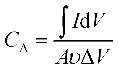
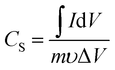
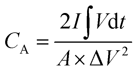
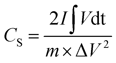
The room-temperature electrochemical response of the synthesized materials was recorded using an electrochemical workstation (CHI 660E). A high-power UV light emitting diode (LED) (365 nm wavelength, 3 W) was used to analyze the energy storage capability under optical illumination. In a three-electrode system, the V2O5/ZnO/FTO sample was used as a working electrode, Ag/AgCl as a reference electrode, and Pt wire as the counter electrode. The electrochemical analysis was performed using 1 M KCl electrolyte solution in the potential range of −0.6 to 0.1 V. The cyclic voltammetry (CV) analyses were conducted under different scan rates (5–100 mV s−1). Galvanostatic charge/discharge (GCD) analyses were conducted under similar voltage limits by varying the current density for charging/discharging. The electrochemical impedance spectroscopy (EIS) was performed in the frequency range of 0.01 Hz to 100 kHz under an alternating current (AC) voltage of 5 mV amplitude.The areal capacitance (CA, F cm−2) was determined from the CV measurements as:20
 | (1) |
 | (2) |
 | (3) |
 | (4) |
 | (5) |
 | (6) |
The coulombic efficiency (η) was calculated from the GCD curve using the following equation:
 | (7) |
2.5 Fabrication of symmetric solid-state supercapacitor
A symmetric type solid-state supercapacitor (SSC) was fabricated using two similar V2O5/ZnO/FTO electrodes. The nontoxic PVA/KCl gel electrolyte was used in the SSC to avoid leakage from the device.23,24 Gel electrolyte was prepared by dissolving 6 g of polyvinyl alcohol (PVA) in 60 ml DI water under stirring at 90 °C for 3 h. Next, 1 M KCl was added to the solution under magnetic stirring until it formed a homogeneous solution. The obtained clear transparent gel electrolyte was cooled to room temperature for further use. Further, a filter paper was dipped into the gel electrolyte for 30 minutes and used as a separator between the two electrodes of SSC. The separator was sandwiched between the electrodes to assemble the device followed by drying in convection oven at 40 °C for 20 h. A digital image of the fabricated device is shown in Fig. S1.†3 Results and discussion
3.1 Morphological analysis
FESEM images were acquired to analyze the morphology of the synthesized nanostructures (Fig. 1). Fig. 1(a) shows densely and uniformly grown ZnO nanorods over the FTO substrate with a clearly visible hexagonal cross-section. The V2O5 coated ZnO nanorods on the FTO substrate are shown in Fig. 1(b), where V2O5 flakes are grown over the ZnO nanorod layer, forming a layered heterostructure. The side view of V2O5 and ZnO layers over FTO is shown in the inset image of Fig. 1(b). The side view of the synthesized ZnO nanorods over the FTO substrate confirms the densely packed vertical growth of nanorods with an average length of ∼2 μm and diameter of ∼300 nm. The energy dispersive X-ray spectroscopy (EDS) revealed the purity, atomic, and weight percentages of elements present in the synthesized materials (Fig. S2†).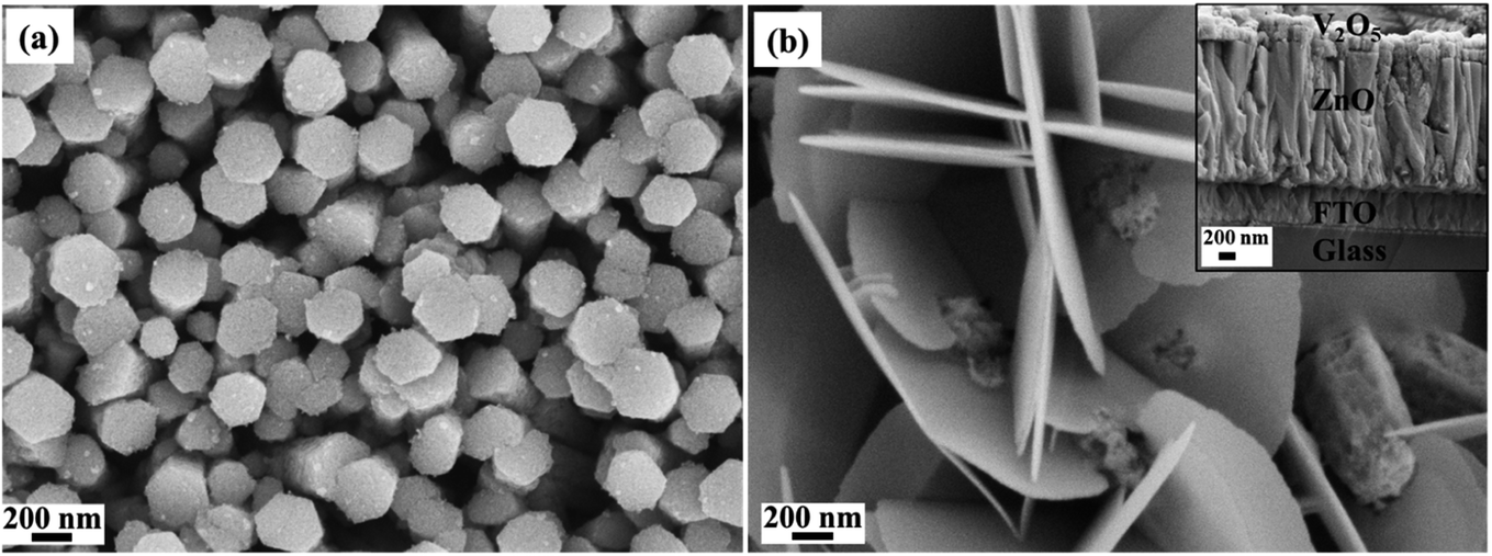 | ||
| Fig. 1 FESEM image showing (a) the ZnO nanorods grown over FTO substrate (top view), (b) V2O5/ZnO over FTO (top view), and a side view of the V2O5/ZnO/FTO electrode (inset image). | ||
3.2 X-ray diffraction analyses
Fig. 2(a) shows the XRD spectrum of ZnO nanorods. The peaks present at 2θ values of 31.8°, 34.4°, 36.2°, 47.5°, 56.6°, 63°, 66.3°, 68.1°, and 69.1° correspond to the (100), (002), (101), (102), (110), (103), (200), (112), and (201) planes, respectively, which are the characteristic planes of the wurtzite ZnO (JCPDS No. 41-1445).25 The preferred growth direction is along the c-axis, as evidenced by the dominant (002) peak at 34.4°.26 This finding is consistent with the FESEM images of the synthesized ZnO/FTO nanostructures. Fig. 2(b) shows the XRD spectrum of the V2O5/ZnO heterostructure grown over the FTO substrate. The V2O5 characteristic XRD peaks are observed at 2θ values of 13°, 19°, 26.7°, 30.6°, and 40.8° and are attributed to the (200), (001), (110), (301), and (102) planes (JCPDS No. 41-1426), respectively.26 The rest of the peaks in Fig. 2(b) belong to ZnO, and the FTO substrate with the ZnO peaks diminished in intensity and slightly shifted due to the heterostructure formation.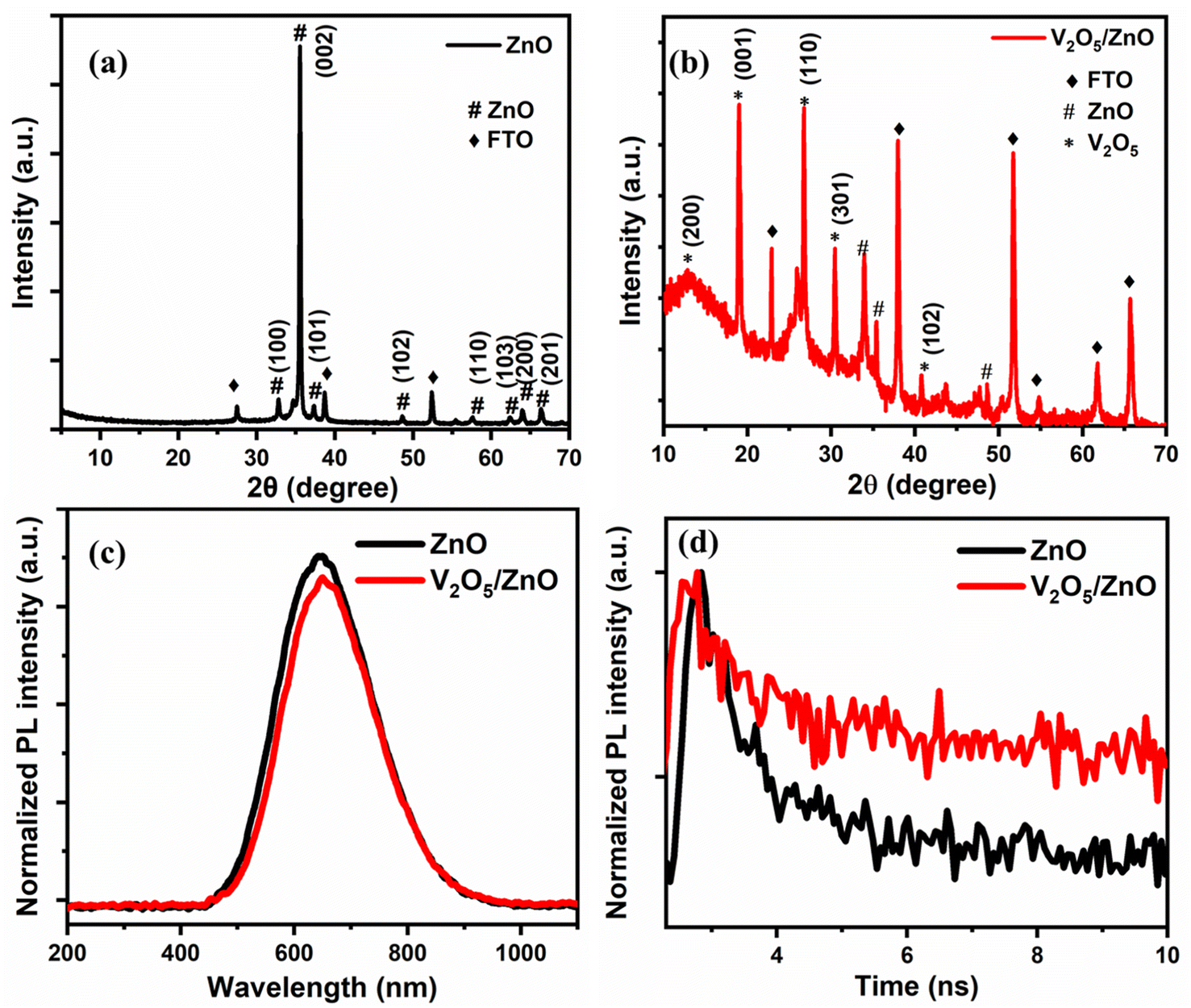 | ||
| Fig. 2 XRD analyses of (a) ZnO and (b) V2O5/ZnO heterostructure synthesized over FTO substrate. (c) Photoluminescence (PL) spectra of ZnO and V2O5/ZnO heterostructure. (d) Time-resolved PL spectra of ZnO and V2O5/ZnO heterostructure. | ||
3.3 Photoluminescence (PL) and time-resolved PL spectroscopy
Fig. 2(c) shows PL spectra of the synthesized ZnO and V2O5/ZnO heterostructure over the FTO substrate. The excitation wavelength for PL measurement was 405 nm. A broad, deep-level emission (DLE) peak corresponding to the recombination of electron–hole associated with intrinsic defect states was observed at ∼640 nm.27 The intrinsic defects of Zn and O vacancies (VZn and VO) are responsible for this type of emission in ZnO nanostructures.28 The peak intensity reduces and slightly red shifts after heterostructure formation with V2O5, which suggests the formation of new energy levels resulting in lower-energy recombination and PL emission. Fig. 2(d) shows the time-resolved PL spectra of ZnO and V2O5/ZnO heterostructure. The lifetime of charge carriers was measured by the exponential fitting of the PL decay curves. The lifetimes of charge carriers for ZnO and V2O5/ZnO heterostructures are 0.83 ns and 1.10 ns, respectively. The increase in the lifetime of charge carriers is desirable and attributed to the formation of a suitable pathway for charge separation in V2O5/ZnO heterostructure. The optical characterization by UV-vis absorbance spectroscopy, Raman analysis, and FTIR spectroscopy are given in Fig. S3–S5.†3.4 Electrochemical analysis
The electrochemical characterization was performed on the synthesized V2O5/ZnO heterostructure grown on the FTO substrate. Here, the conducting surface of the FTO glass (on which the stacked nanostructures of ZnO and V2O5 were grown) serves as a current collector. As mentioned in Section 2.4, the V2O5/ZnO/FTO is the working electrode in the three-electrode system, and two similar electrodes were used as the anode and cathode in the symmetrical SSC. The schematic representation shown in Fig. 3 describes the various steps involved in SSC fabrication, starting from the growth of layered nanostructures over FTO, followed by the assembly of two similar electrodes. The encircled section in the device schematic shows different layers of substrate, nanomaterials, and separator.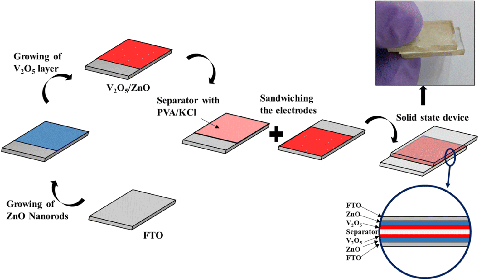 | ||
| Fig. 3 Schematic representation explains the fabrication steps involved in the solid-state device fabrication using V2O5/ZnO as the energy-storing material and the digital image of the device. | ||
The electrochemical performance of the prepared V2O5/ZnO/FTO heterostructure was analyzed by a three-electrode measurement system with 1 M KCl as an electrolyte solution (as mentioned in Section 2.4). Fig. 4(a) shows the CV curves in the potential range of −0.6 to 0.1 V (vs. Ag/AgCl) at a scan rate of 10 to 100 mV s−1. The CV curves do not show any specific peaks during anodic and cathodic sweeps, implying presence of electrostatic double layer capacitance behavior wherein the electrical charge storage is stored electrostatically with no redox reaction between the heterostructure and the ions. The GCD characteristics of the electrode were measured at different current densities in the potential window of −0.6 to 0.1 V vs. Ag/AgCl, as shown in Fig. 4(b). The areal, CA and specific capacitances, CS of the electrode were measured from the GCD curves and are shown in Fig. 4(c) and (d), respectively. The calculated CA values are 2.22, 1.82, 0.73, 0.49, and 0.36 mF cm−2 at the current densities of 30, 40, 60, 80, and 100 μA cm−2, respectively. Similarly, the obtained CS values are 89.14, 72.81, 29.38, 19.72, and 14.7 mF g−1 at a specific current of 1.2, 1.6, 2.4, 3.2, and 4 mA g−1, respectively. These values are significantly higher than the previous literature and are attributed to the novel stacked configuration of the metal oxide nanostructures over the FTO substrate.29–32 We also measured the electrochemical performance of the synthesized electrode in the positive potential range of 0.1 to 0.9 V vs. Ag/AgCl, and the results are shown in Fig. S6.† The coulombic efficiency of the V2O5/ZnO/FTO heterostructure at different current densities (from Fig. 4(b)) is shown in Fig. S7.† Clearly, the coulombic efficiency of V2O5/ZnO/FTO heterostructure is very high for low current density values (∼152% at 30 μA cm−2). Also, at higher current densities, the coulombic efficiency remains above 100% (∼120% at 100 μA cm−2).
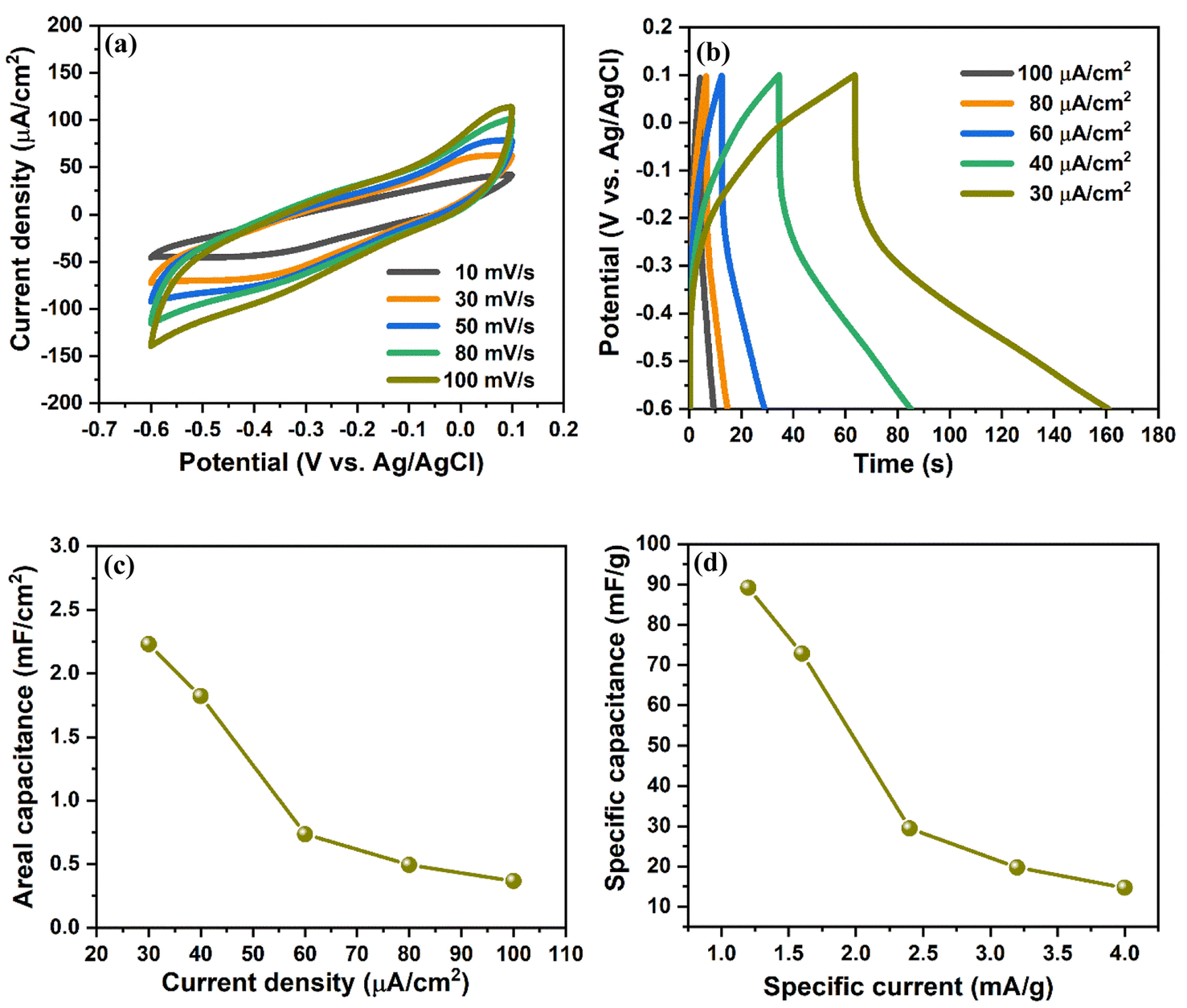 | ||
| Fig. 4 Electrochemical analysis of V2O5/ZnO/FTO heterostructure via three-electrode measurement system in the potential range of −0.6 to 0.1 V by (a) CV measurements at different scan rates, (b) GCD plots at different current densities, (c) areal capacitance, and (d) specific capacitance calculated from GCD curve at different current densities. | ||
The electrochemical performance of V2O5/ZnO/FTO-based SSC was measured by performing the CV, GCD, and EIS. Fig. 5(a) shows the CV response of the SSC for different scan rates, which shows a quasi-rectangular profile without any redox peak, implying the EDLC behavior of the device. An increase in the peak current values with increasing scan rates is evident from the CV analysis, suggesting good charge storage properties at the surface of the V2O5/ZnO heterostructure. The contribution of surface capacitive and diffusion-controlled charge storage in the device were calculated from capacitive component (k1ν), and diffusion component (k2ν1/2) by measuring the current (i) at a fixed voltage from the CV curves as:33
| i(V) = k1ν + k2ν1/2 | (8) |
| i(V)/ν1/2 = k1ν1/2 + k2 | (9) |
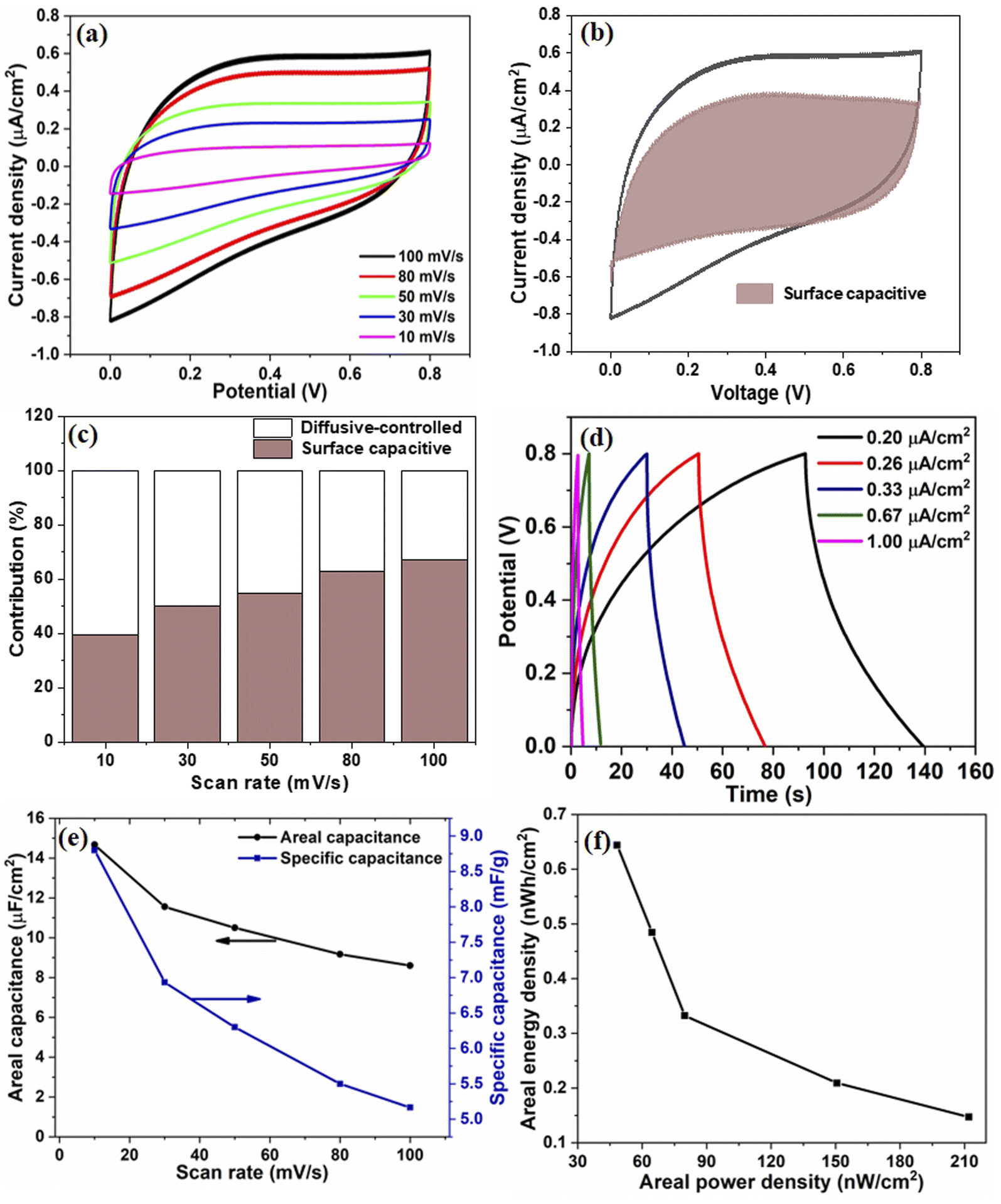 | ||
| Fig. 5 Electrochemical analyses of V2O5/ZnO/FTO-based SSC. (a) CV analysis at different scan rates and (b) capacitive and diffusion-controlled contributions in the charge storage at 100 mV s−1 scan rate, (c) percentage contribution of capacitive and diffusion-controlled charge storage at different scan rates, (d) GCD plots at different current densities, (e) areal and specific capacitances for scan rates used in (a) and (f) energy density vs. power density curve calculated from the CD curve. | ||
These values were calculated for all voltages used in the CV analysis, and the corresponding curve for the 100 mV s−1 scan rate is shown in Fig. 5(b). The percentage capacitive contribution at scan rates of 10, 30, 50, 80, and 100 mV s−1 were ∼39.4, 50, 54.7, 63, and 67.1%, respectively, as shown in Fig. 5(c). The increase in the surface capacitive contribution is due to the charge stored at the electrode surface because less time is available for ion diffusion at higher scan rates.34
The GCD data in Fig. 5(d) depicts the charging and discharging behaviors of the device at different current densities in the same potential window as the CV data. An increase in the charging/discharging times with the decrease in current densities was observed. A sufficiently high discharge time under all the current densities adds to the efficient performance of the device. The CA and CS values calculated from CV curves are shown in Fig. 5(e). As expected, at lower scan rates, the capacitance values are higher due to ample intercalation time for the ions into the active material's nanostructure. Additionally, the sharp edges and surface irregularities of the nanostructures contribute to the enhanced surface area and interaction sites for charge storage.35 The areal capacitance of the device is also calculated from the GCD curves and shown in Fig. S8.† The corresponding energy and power density values are calculated and shown in Fig. 5(f).
In situ photo-electrochemical responses of the fabricated SSC under UV illumination (365 nm) deduced from CV, GCD, and EIS analysis are shown in Fig. 6. Fig. 6(a) shows the CV curves under dark and UV-illuminated conditions at 50 mV s−1. Clearly, the current density increases throughout the potential sweep under UV exposure. The same trend was obtained for the 80 mV s−1 scan rate, as shown in Fig. S9.† Additionally, it increases the area enclosed by the curve, and an enhanced CA of ∼65% is observed under UV illumination. The reason for enhanced hysteresis can be attributed to the photogenerated charges. In the presence of UV radiation, the valence band electrons in the metal oxide semiconducting material are photo-excited. Electrons jump from the valence band to the conduction band and are conducted away through the external circuit. At the same time, the holes are left behind in the valence band. The continuously increasing current density with an increase in the potential results in a larger CV area, which can be attributed to the continuous electron and hole generation under UV light.36,37 The asymmetric shape of the CV curve is due to the UV illumination of the electrode from one side. The photogenerated electrons transfer to the other electrode from the outer circuit and help in charge separation. The adsorbed oxygen (O2−) at the surface of metal oxide nanostructures plays a critical role in increasing the current flow. Photogenerated electrons are transferred to the current collector while holes react with O2− and generate additional electrons (O2− + h+ → O2 + e−). At the same time, a few holes are trapped at the hole-trapping sites (Zn ion vacancies) of ZnO, which promotes the separation of charges. This increases the effective density of charge carriers at the interface and reduces the depletion width.36
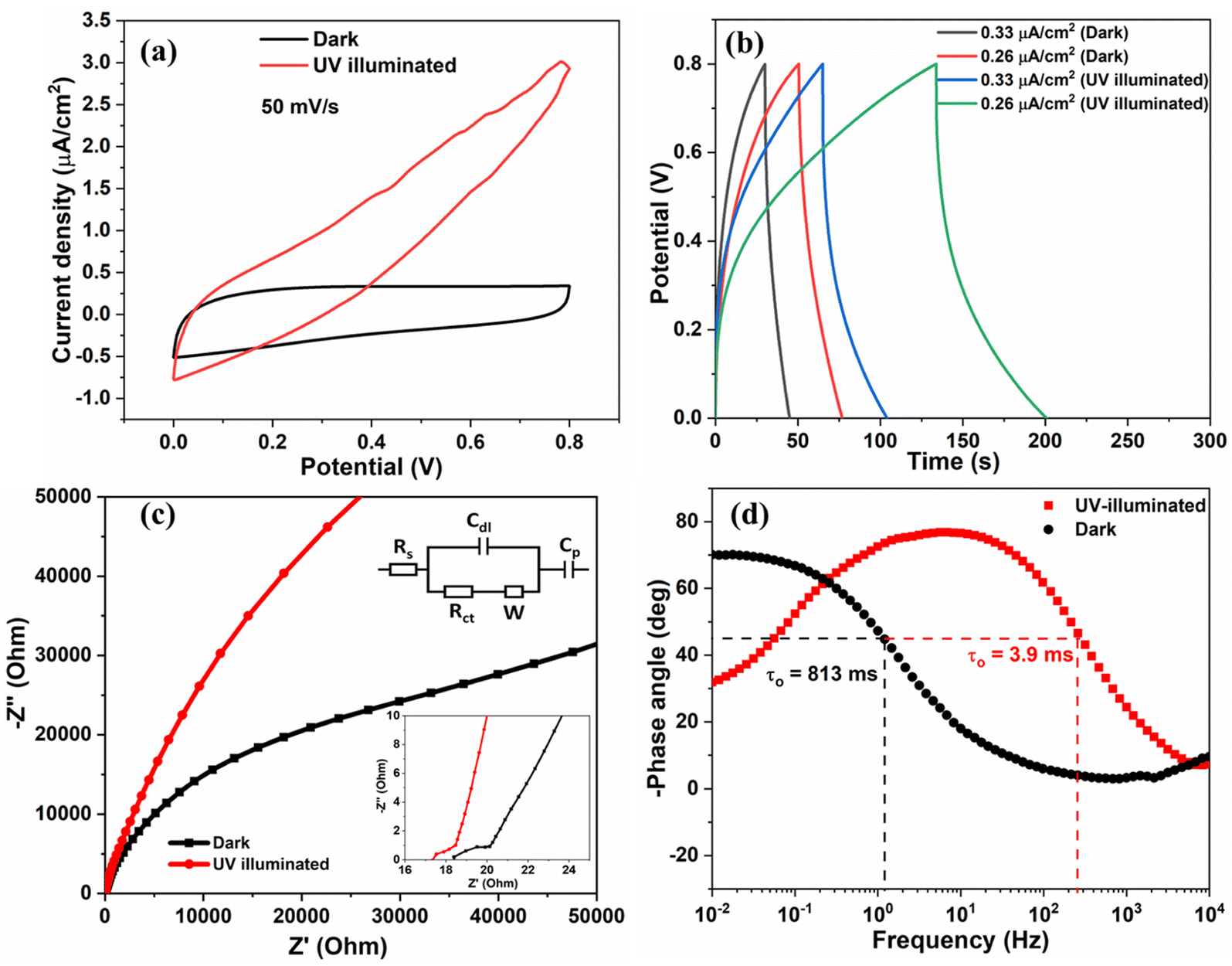 | ||
| Fig. 6 (a) Light-induced CV response of the V2O5/ZnO/FTO symmetrical SSC at 50 mV s−1, (b) GCD curve at different current densities, (c) Nyquist plots and corresponding equivalent circuit diagram (inset images), and (d) Bode plot (−phase angle vs. frequency) of the SSC under dark and UV-illuminated conditions. | ||
The GCD study conducted under UV light also suggests enhanced charge and discharge times, as shown in Fig. 6(b). The discharge time has significantly increased, irrespective of the current density. The charge and discharge times increased due to more number of electrons and resulting ion interaction with the active material under UV illumination.
Fig. 6(c) shows the Nyquist plot of the device before and after exposure to the UV light, and the corresponding equivalent circuit is shown in the inset image. In the high-frequency region, the intersection of the resultant Nyquist plot with the real axis represents Rs (total equivalent series resistance). Rs contains the effect of combined resistance from contact resistance between the current collector and electrode material, resistance at the interface of the electrode material and electrolyte, inherent resistance due to electrode material, and resistance of the electrolyte ions in the solution.38 The electrical double-layer capacitance is represented by Cdl, and linear portion is called frequency-dependent Warburg impedance (W). Cp represents the pseudocapacitance considering possible redox reactions offered by V2O5/ZnO defects. There is a slight decrease in the charge transfer resistance, Rct (from ∼1.6 Ω to ∼0.81 Ω) and Rs varied from ∼18.4 Ω to 17.3 Ω. The Bode plot (−phase angle vs. frequency) is shown in Fig. 6(d), plotted using EIS data. The maximum phase angle of the device under UV illumination reaches 77.8°, which is more than the maximum phase angle obtained under the dark condition (70.3°). The phase angle closer to 90° signifies the more capacitive behavior of the supercapacitor. Additionally, we calculated the relaxation time constant (τo) of the device, which depends upon the characteristic frequency (fo) corresponding to 45° phase angle. The relaxation time constant (τo = 1/fo) is the time required to discharge the device with greater than 50% efficiency. The τo value under UV irradiation is 3.9 ms which is very small in comparison to the τo under the dark condition (813 ms). The low relaxation time constant values under UV light signify faster ion diffusion and charge storage characteristics of the supercapacitor device. In the dark condition, the double layer dynamics is governed only by the ionic diffusion in the electrolyte towards the double layer (as there is no electron–hole pair separation in the heterostructure). Since diffusion is a slow process, lower frequencies (higher time periods) lead to higher charge storage, thus leading to increased capacitance and a higher phase angle (in magnitude). Under UV illumination, the double layer dynamics is governed by the interplay of four processes, viz., electron–hole pair generation and charge carrier separation, electron–hole pair recombination in the heterostructure, the reaction of holes with the oxide ions, and ionic diffusion in the electrolyte.
Electron–hole pair separation depends on the electronic conduction through the heterostructure to the external circuit. While ionic diffusion is a slow process, electronic conduction is expected to be relatively faster. Moreover, low frequencies (larger time periods) also increase the probability of electron–hole pair recombination, which can still occur if the recombination rate is faster than the rate kinetics for the reaction between holes and oxide ions. This interplay leads to the reduction in the phase angle at low frequencies under UV-illuminated conditions.
The charge storage mechanism is elucidated with the help of schematic diagrams in Fig. 7. When the UV light illuminates the electrode materials (V2O5 and ZnO) through the FTO substrate, the electrons (e−) present in the valence band (VB) of the semiconducting metal oxides jump to the conduction band (CB) and leave holes (h+) in VB. Due to the difference in conduction band minima of the two materials, the photogenerated e− are transferred from V2O5 CB to ZnO CB and finally to the external circuit via FTO.39
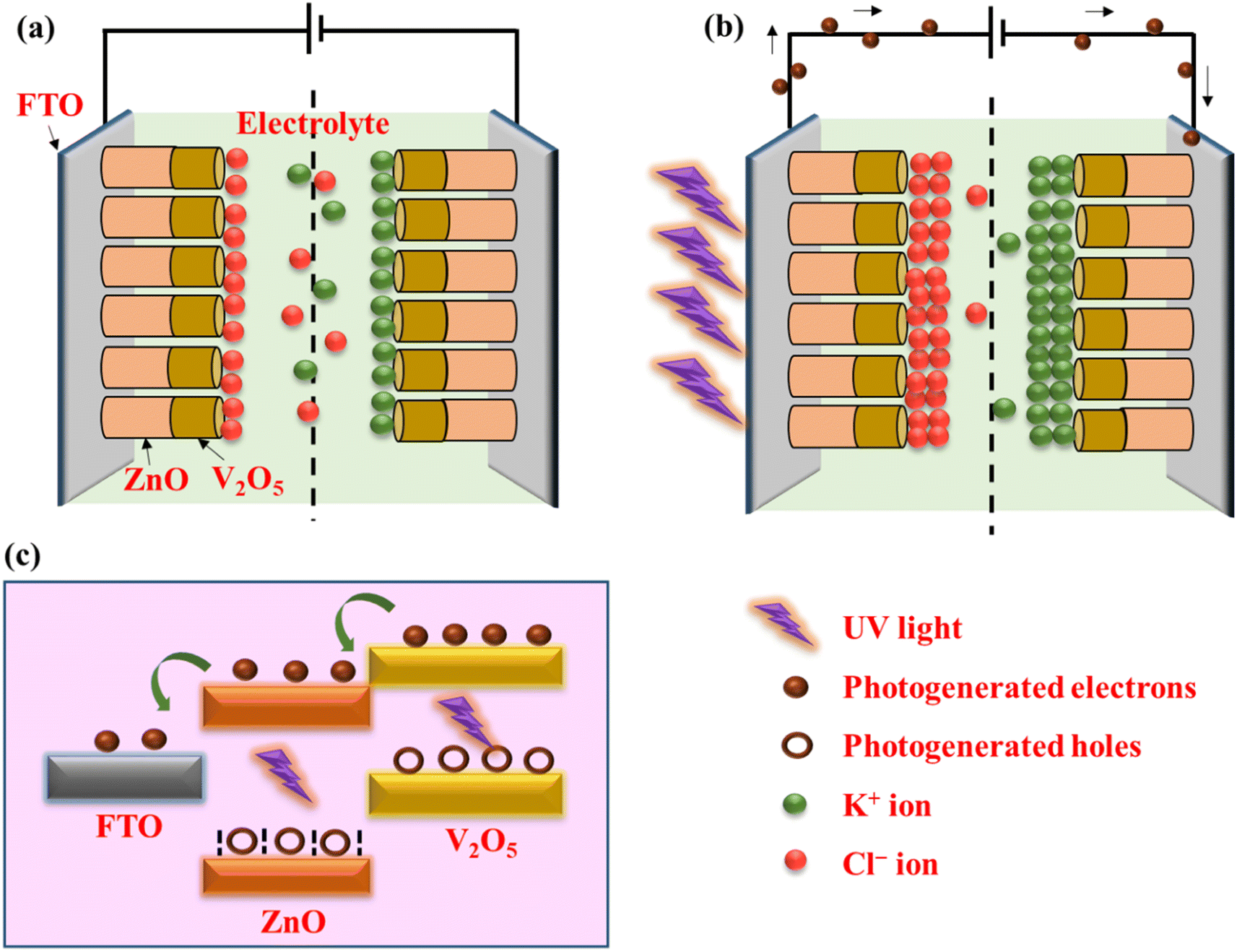 | ||
| Fig. 7 Schematic diagram of charge storage mechanism under (a) dark and (b) UV-illuminated conditions. (c) Band diagram showing the flow of photogenerated electrons under UV illumination. | ||
The holes left behind in VB are trapped in the hole-trapping sites of ZnO (such as Zn ion vacancies). Similarly, the photogenerated holes at VB of V2O5 also get accumulated. Hence, the separation of e− and h+ occurs during photo-charging due to the SSC's unique heterostructure. The accumulated h+ creates a positive polarity at the electrode and attracts Cl− ions from the electrolyte. On the other hand, the photogenerated e− transferred to the other electrode creates negative polarity and attracts K+ ions. Hence, double-layer capacitance is formed at the two electrodes causing surface capacitance build-up, which is enhanced by UV illumination. The unique and reversible ion intercalation/deintercalation property of layered V2O5 nanostructure is further utilized to store and release the ions during charging and discharging cycles.
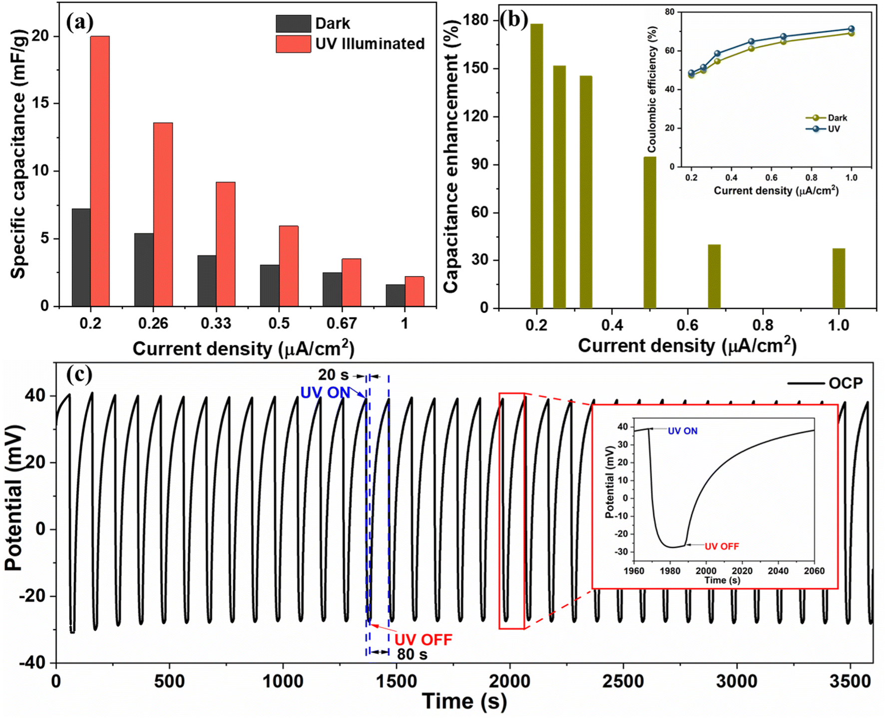
The Cs values under UV illumination are 20, 13.6, 9.75, 3.5, and 2.6 mF g−1 at the current density of 0.2, 0.26, 0.33, 0.5, 0.6, and 1 μA cm−2, respectively, and are compared with dark condition Cs value (Fig. 8(a)). We obtained ∼178%, 152%, 145%, 95%, 40%, and 38% enhancement in the CS measured from the GCD curve at 0.2, 0.26, 0.33, 0.6, and 1 μA cm−2, respectively, by exposing the device to the UV light as shown in Fig. 8(b). The significant improvement in the charge storage capacity of the device is attributed to the enhanced charge separation and uniform heterostructure formation during a layered growth of the active materials (ZnO and V2O5). The coulombic efficiency of the device was also measured in the dark and UV-illuminated conditions, and the results are shown in the inset image of Fig. 8(b). The coulombic efficiency under UV-illuminated conditions is higher than the dark condition, which can be attributed to the faster charging in comparison to discharging due to photogenerated charges under UV illumination.
 | ||
| Fig. 8 Comparison of specific capacitance at different current densities under UV and dark conditions, (b) percentage enhancement in specific capacitance at different current densities and comparison of coulombic efficiencies at different current densities under dark and UV (inset image) and (c) OCP variation with respect to time under cyclic UV illumination (the inset image shows a single cycle). | ||
Further, the open circuit potential (OCP) of the device was measured with respect to time by illuminating it cyclically with UV light (20 s ON and 80 s OFF) (shown in Fig. 8(c)). We observed that on UV illumination, the OCP drops from 0.040 V to −0.035 V in 20 s and recovers back to its original value in 80 s after turning OFF the UV light. On UV illumination, the electrons from the valence band of metal oxides (V2O5/ZnO) jump to the conduction band. The photogenerated electrons move toward the external circuit via conducting path provided by FTO, and the holes are left in the valence band.40 Due to the increase in the number of electrons in the conduction band after UV illumination, a drop in OCP is recorded, which was recovered in the dark condition. This observation was repeated for several ON/OFF cycles and was found to be consistent throughout the measurement. The enhanced charge separation achieved during UV illumination is evident from this analysis, and it supports our study regarding the high capacitance response of the supercapacitor device under UV light.
The cyclic stability of the device is measured by charging and discharging at 0.67 μA cm−2 current density and 0 to 0.8 V potential window for 5000 cycles (shown in Fig. 9(a)). Good stability of the device can be observed as the specific capacitance value remains stable for 2000 cycles, beyond which an increment from ∼2.5 mF g−1 to ∼4.8 mF g−1, as shown in Fig. 9(b). Many researchers have reported an increase in supercapacitor device capacitance in the past.41,42 The reason for such behavior can be attributed to the activation of the material after a certain number of cycles which is a commonly observed phenomenon for metal oxides.43 As per a few studies, the removal of oxygen functional groups and improved access of ions to pores of active material after a few cycles contributes to increased capacitance.41 The percentage capacitance retention of the device under dark and UV-illuminated conditions is shown in Fig. S10.† The 5000 cycles of charging and discharging of the device under UV light showed a reduction in capacitance retention of the device. The capacitance retention reaches ∼78% and remains stable. The continuous exposure to UV light results in crosslinking of PVA/KCl electrolyte, which may affect the ion transport characteristics of the electrolyte.44,45 We also measured the coulombic efficiency of the supercapacitor after different cycle numbers, as shown in Fig. 9(c). Initially, the device shows coulombic efficiency of 78%, which increases to ∼95% after 200 cycles of charge–discharge and remains stable.
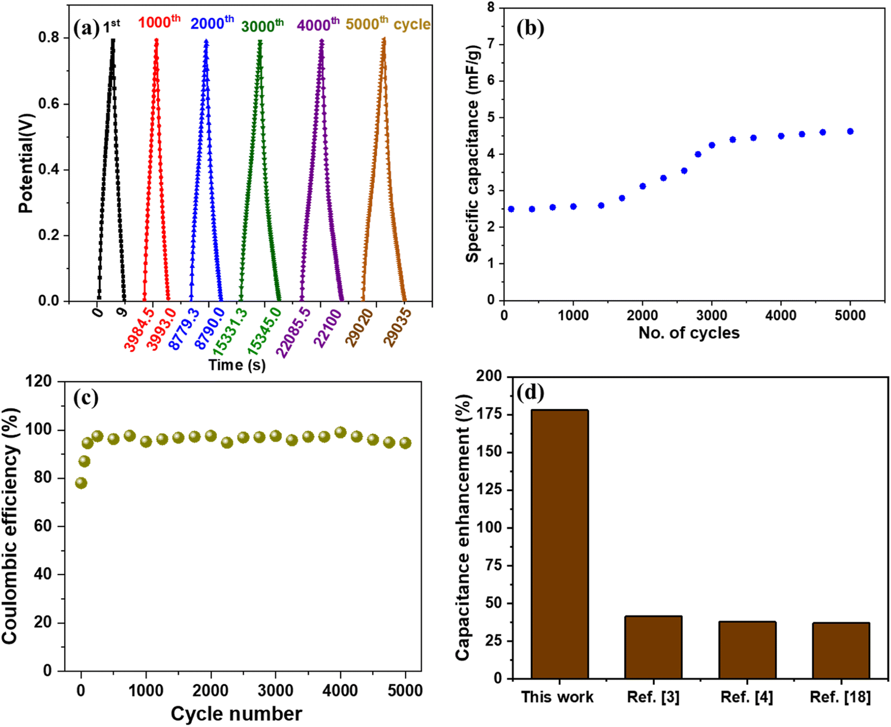 | ||
| Fig. 9 (a) GCD plot of the device for 1000th, 2000th, 3000th, 4000th, and 5000th cycle at 0.67 μA cm−2 current density, (b) cyclic stability in terms of specific capacitance variation with respect to the number of cycles of charge–discharge, (c) coulombic efficiency of the supercapacitor after cycling, and (d) maximum capacitance enhancement under UV irradiation in comparison with other studies. | ||
To analyze the effect of electrochemical cycles on the morphology and chemical structure of the V2O5/ZnO/FTO heterostructure, we conducted the SEM, XRD, and FTIR analysis before and after 3000 electrochemical cycles (under dark), and the results are shown in Fig. S11.† We observed that there a small distorted morphology of the heterostructure after the electrochemical cycles. After electrochemical cycles, the structural integrity remains stable, and no removal of material was observed. The XRD analysis shows a change in intensity and slight shifting of initially observed peaks (for V2O5 and ZnO) which may be due to the intercalation of electrolyte ions into the interlayer of V2O5 and ZnO nanostructure. Some additional peaks belong to the formation of ZnCl2, KCl, and chloride lamellar phase of ZnO.46–48 The FTIR analysis shows the variation in original peaks after electrochemical cycles. In the FTIR spectra before electrochemical cycles, the characteristic peaks of ZnO and V2O5 can be clearly observed at 670, 720, 790, 830, and 960 cm−1.16,49 The peaks observed at 932, 1020, and 1080 cm−1 corresponds to –OH and C–O groups present in the nanostructure of metal oxides. As reported in previous studies, these peaks were found to be reduced in intensity due to interaction with electrolyte ions.50
It is very difficult to compare this work with other studies because there is a huge difference in various parameters such as type of material, electrolyte, synthesis method, heterostructure, electrolyte concentration, device fabrication method, and testing procedure/parameters. However, we compared our results with similar studies considering different parameters and found that our device performed better. For example, we compared various studies with photo-responsive materials and collected the values of maximum percentage enhancement in capacitance or capacity value under the photo-illuminated condition, as shown in Fig. 9(d). We observed that our device shows the highest percentage enhancement (178%) in capacitance value compared to the other optically chargeable supercapacitor devices.3,4,18 The device achieved a maximum energy density of 1.8 nW h cm−2 and a power density of 80 nW cm−2 under UV light illumination. Although, energy and power densities are low, the device shows the highest response for UV illumination compared with other works, as shown in Fig. 9(d). However, the obtained energy density is more than some of the devices based on graphene thin films,51,52 perovskite thin film,53 and SiN nanowires.54 We have also tabulated (Table S1†) the comparison of the areal capacitance of our device with other studies and found that our device performs better than most of the previously reported devices. We also compared the capacitance of our electrode material with other works which use similar materials and electrolytes. Our V2O5/ZnO/FTO electrode shows a maximum areal capacitance of 3.3 mF cm−2 at 20.83 μA cm−2, which is more than ZnO/ITO (0.65 mF cm−2 at 100 mV s−1),32 ZnO/FTO (21 μF cm−2 at 50 mV s−1),55 ZnO/MnO2/FTO (2.5 mF cm−2 at 0.1 mA cm−2),56 SWCNT/ZnO (1.53 mF cm−2 at 1.25 μA cm−2),3 and BR/P3HT/ITO (2.44 mF cm−2 at 20 μA cm−2).57 We did not prefer carbon-based materials to improve the performance of the device to avoid the issues related to complex synthesis methods, loss of optical response, agglomeration of the material, and toxicity.
Conclusions
In summary, we synthesized a novel layered optically responsive metal oxide heterostructure (V2O5/ZnO) over an optically transparent FTO substrate and successfully utilized it to fabricate a symmetric solid-state supercapacitor. The hydrothermal synthesis process followed by annealing created uniformly distributed ionic defects (oxygen vacancies) which were utilized during charge storage. At the same time, the layered structure of V2O5 allowed facile intercalation of electrolyte ions. Under UV illumination, the photogenerated electrons are separated from holes due to the different work functions of the two materials. These combined effects resulted in the excellent electrochemical performance of the device. The fabricated supercapacitor device showed efficient conversion of light energy (365 nm UV) into electrochemical energy and resulted in ∼178% increment in the specific capacitance value at 0.2 μA cm−2 current density. The device showed outstanding cyclic stability up to 5000 cycles with improved specific capacitance over time. In our opinion, this work provides an advanced approach to utilizing light energy in energy storage devices for modern applications.Conflicts of interest
There are no conflicts to declare.Acknowledgements
All the authors would like to acknowledge Centre for Nanoscience and Engineering, Indian Institute of Science (IISc) for providing characterization facilities. Prof. AM and Prof. AMR acknowledge the funding from IUSSTF/JC-146/2019. PSC acknowledges the research grant received under CV Raman postdoctoral fellowship (grant no. IE/REAC-21-0202.26).References
- A. Tyagi, K. M. Tripathi and R. K. Gupta, J. Mater. Chem. A, 2015, 3, 22507–22541 RSC.
- E. Samuel, P. U. Londhe, B. Joshi, M. W. Kim, K. Kim, M. T. Swihart, N. B. Chaure and S. S. Yoon, J. Alloys Compd., 2018, 741, 781–791 CrossRef CAS.
- R. Sinha, N. Roy and T. K. Mandal, Chem. Eng. J., 2022, 431, 133915 CrossRef CAS.
- C. An, Z. Wang, W. Xi, K. Wang, X. Liu and Y. Ding, J. Mater. Chem. A, 2019, 7, 15691–15697 RSC.
- B. Zhang, J. Zheng, L. W. Ma, B. Guo, X. C. He, M. J. Gao, L. Bian, X. F. Ma and G. Li, Mater. Sci. Forum, 2016, 847, 203–210 Search PubMed.
- A. K. Jena, A. Kulkarni and T. Miyasaka, Chem. Rev., 2019, 119, 3036–3103 CrossRef CAS.
- Y. Akila, N. Muthukumarasamy and D. Velauthapillai, in Nanomaterials for Solar Cell Applications, Elsevier, 2019, pp. 127–144 Search PubMed.
- X. Xu, J. Tang, H. Qian, S. Hou, Y. Bando, M. S. A. Hossain, L. Pan and Y. Yamauchi, ACS Appl. Mater. Interfaces, 2017, 9, 38737–38744 CrossRef CAS PubMed.
- L. Chen, X. Xu, L. Wan, G. Zhu, Y. Li, T. Lu, M. D. Albaqami, L. Pan and Y. Yamauchi, Mater. Chem. Front., 2021, 5, 3480–3488 RSC.
- Y. Li, G. Zhu, X. Xu, L. Chen, T. Lu, J. P. Hill, L. Pan and Y. Yamauchi, Small Struct., 2022, 3, 2200015 CrossRef CAS.
- D. Lee, S. Mathur and K. H. Kim, Nano Energy, 2021, 86, 106076 CrossRef CAS.
- S. K. Sharma, G. Sharma, A. Gaur, A. Arya, F. S. Mirsafi, R. Abolhassani, H.-G. Rubahn, J.-S. Yu and Y. K. Mishra, Energy Adv., 2022, 1, 457–510 RSC.
- T. Hou, M. Ali, R. Boppella, M. Afifi, S. J. Patil, S. Ryu and D. Lee, J. Energy Chem., 2020, 49, 262–274 CrossRef.
- R. K. Mishra, G. J. Choi, H. J. Choi, J. Singh, F. S. Mirsafi, H. G. Rubahn, Y. K. Mishra, S. H. Lee and J. S. Gwag, Chem. Eng. J., 2022, 427, 131895 CrossRef CAS.
- A. Wibowo, M. A. Marsudi, M. I. Amal, M. B. Ananda, R. Stephanie, H. Ardy and L. J. Diguna, RSC Adv., 2020, 10, 42838–42859 RSC.
- P. S. Chauhan, R. Kant, A. Rai, A. Gupta and S. Bhattacharya, Mater. Sci. Semicond. Process., 2019, 89, 6–17 CrossRef CAS.
- V. S. Bhati, M. Hojamberdiev and M. Kumar, Energy Reports, 2020, 6, 46–62 CrossRef.
- H. Li, M. Wang, G. Qi, Y. Xia, C. Li, P. Wang, M. Sheves and Y. Jin, J. Mater. Chem. A, 2020, 8, 8268–8272 RSC.
- A. Gupta, S. S. Pandey, M. Nayak, A. Maity, S. B. Majumder and S. Bhattacharya, RSC Adv., 2014, 4, 7476–7482 RSC.
- S. Kumar and A. Misra, Nanoscale, 2021, 13, 19453–19465 RSC.
- P. Sundriyal and S. Bhattacharya, ACS Appl. Energy Mater., 2019, 2, 1876–1890 CrossRef CAS.
- S. Kumar, S. Telpande, V. Manikandan, P. Kumar and A. Misra, Nanoscale, 2020, 12, 19438–19449 RSC.
- J. Zhu, Y. Xu, J. Wang, J. Lin, X. Sun and S. Mao, Phys. Chem. Chem. Phys., 2015, 17, 28666–28673 RSC.
- A. Pullanchiyodan, L. Manjakkal, S. Dervin, D. Shakthivel and R. Dahiya, Adv. Mater. Technol., 2020, 5, 1901107 CrossRef CAS.
- A. Kathalingam, V. Senthilkumar, S. Valanarasu and J. K. Rhee, Semicond. Sci. Technol., 2012, 27, 105006 CrossRef.
- T. F. Hou, M. A. Johar, R. Boppella, M. A. Hassan, S. J. Patil, S. W. Ryu and D. W. Lee, J. Energy Chem., 2020, 49, 262–274 CrossRef.
- D. Kumbhar, S. Delekar, S. Kumbhar, A. Dhodamani, N. Harale, R. Nalawade and A. Nalawade, Chem. Pap., 2021, 75, 4001–4017 CrossRef CAS.
- A. K. Singh, G. S. Thool, P. R. Bangal, S. S. Madhavendra and S. P. Singh, Ind. Eng. Chem. Res., 2014, 53, 9383–9390 CrossRef CAS.
- A. Guerra, A. Achour, S. Vizireanu, G. Dinescu, S. Messaci, T. Hadjersi, R. Boukherroub, Y. Coffinier and J. J. Pireaux, Appl. Surf. Sci., 2019, 481, 926–932 CrossRef CAS.
- M. Singh, K. Manoli, A. Tiwari, T. Ligonzo, C. Di Franco, N. Cioffi, G. Palazzo, G. Scamarcio and L. Torsi, J. Mater. Chem. C, 2017, 5, 3509–3518 RSC.
- N. Venugopal, B. C. Yang and T. Ko, Mater. Res. Innovations, 2012, 16, 96–100 CrossRef CAS.
- A. H. Ismail, A. H. Abdullah and Y. Sulaiman, Superlattices Microstruct., 2017, 103, 171–179 CrossRef CAS.
- J. Wang, J. Polleux, J. Lim and B. Dunn, J. Phys. Chem. C, 2007, 111, 14925–14931 CrossRef CAS.
- Y. Li, Y. Meng, M. Xiao, X. Liu, F. Zhu and Y. Zhang, J. Mater. Sci.: Mater. Electron., 2019, 30, 12659–12668 CrossRef CAS.
- P. S. Chauhan and S. Bhattacharya, Mater. Lett., 2018, 217, 83–87 CrossRef CAS.
- M. Lu, M. Lu, S. You, C. Chen and Y. Wang, Sci. Rep., 2015, 5, 15123 CrossRef CAS PubMed.
- A. Qian, K. Zhuo, P. K. Kannan and C. Chung, ACS Appl. Mater. Interfaces, 2016, 8, 34455–34463 CrossRef CAS.
- Z. Fan, J. Yan, T. Wei, L. Zhi, G. Ning, T. Li and F. Wei, Adv. Funct. Mater., 2011, 21, 2366–2375 CrossRef CAS.
- R. Saravanan, V. K. Gupta, E. Mosquera and F. Gracia, J. Mol. Liq., 2014, 198, 409–412 CrossRef CAS.
- M. Haro, L. F. Velasco and C. O. Ania, Catal. Sci. Technol., 2012, 2, 2264–2272 RSC.
- S. T. Senthilkumar, R. K. Selvan, Y. S. Lee and J. S. Melo, J. Mater. Chem. A, 2013, 1, 1086–1095 RSC.
- M. Maher, S. Hassan, K. Shoueir, B. Yousif and M. E. A. Abo-Elsoud, J. Mater. Res. Technol., 2021, 11, 1232–1244 CrossRef CAS.
- K. Prasad, G. R. Reddy, M. Rajesh, P. Reddi Babu, G. Shanmugam, N. John Sushma, M. Siva Pratap Reddy, B. D. P. Raju and K. Mallikarjuna, Crystals, 2020, 10, 566 CrossRef CAS.
- B. Zhang, R. Shi, Y. Zhang and C. Pan, Prog. Nat. Sci.: Mater. Int., 2013, 23, 164–169 CrossRef.
- T. Sheela, R. F. Bhajantri, V. Ravindrachary, S. G. Rathod, P. K. Pujari, B. Poojary and R. Somashekar, Radiat. Phys. Chem., 2014, 103, 45–52 CrossRef CAS.
- M. Mrad, B. Chouchene and T. Ben Chaabane, S. Afr. J. Chem., 2018, 71, 103–110 CrossRef CAS.
- M. Li, Y. Liu, W. Han, S. Wang, M. Zhang, Y. Yan and W. Shi, Metall. Mater. Trans. B, 2014, 46 Search PubMed.
- X. Lu, G. Li, J. Y. Kim, J. P. Lemmon, V. L. Sprenkle and Z. Yang, Energy Environ. Sci., 2013, 6, 1837–1843 RSC.
- P. S. Chauhan, K. Kumar, K. Singh and S. Bhattacharya, Synth. Met., 2022, 283, 116981 CrossRef CAS.
- W. W. Mar and E. Somsook, ScienceAsia, 2012, 38, 90–94 CAS.
- P. Xu, J. Kang, J. B. Choi, J. Suhr, J. Yu, F. Li, J. H. Byun, B. S. Kim and T. W. Chou, ACS Nano, 2014, 8, 9437–9445 CrossRef CAS PubMed.
- Y. Gao, Y. S. Zhou, W. Xiong, L. J. Jiang, M. Mahjouri-Samani, P. Thirugnanam, X. Huang, M. M. Wang, L. Jiang and Y. F. Lu, APL Mater., 2013, 1 Search PubMed.
- I. Popoola, M. Gondal, L. Oloore, A. J. Popoola and J. AlGhamdi, Electrochim. Acta, 2020, 332, 1–14 CrossRef.
- F. Thissandier, A. Le Comte, O. Crosnier, P. Gentile, G. Bidan, E. Hadji, T. Brousse and S. Sadki, Electrochem. Commun., 2012, 25, 109–111 CrossRef CAS.
- H. Ghannam, J. P. B. Silva and A. Chahboun, RSC Adv., 2021, 11, 23346–23354 RSC.
- C. J. Raj, M. Rajesh, R. Manikandan, J. Y. Sim, K. H. Yu, S. Y. Park, J. H. Song and B. C. Kim, Electrochim. Acta, 2017, 247, 949–957 CrossRef CAS.
- W. J. Dong, W. S. Cho and J. L. Lee, ACS Appl. Mater. Interfaces, 2021, 13, 22676–22683 CrossRef CAS.
Footnote |
| † Electronic supplementary information (ESI) available. See DOI: https://doi.org/10.1039/d2ta06790k |
| This journal is © The Royal Society of Chemistry 2023 |