
Nanostructured doping of WSe2via block copolymer patterns and its self-powered photodetector application
Miae
Kang†
a,
Ki Hyun
Kim†
a,
Joona
Bang
 *a and
Jihyun
Kim
*b
*a and
Jihyun
Kim
*b
aDepartment of Chemical and Biological Engineering, Korea University, Seoul 02841, Republic of Korea. E-mail: joona@korea.ac.kr
bSchool of Chemical and Biological Engineering, Seoul National University, Seoul 08826, Republic of Korea. E-mail: jihyunkim@snu.ac.kr
First published on 26th December 2022
Abstract
Transition metal dichalcogenides (TMDs), e.g., MoS2, MoSe2, ReS2, and WSe2, are effective materials for advanced optoelectronics owing to their intriguing optical, structural, and electrical properties. Various approaches for manipulating the surface of the TMDs have been suggested to unleash the optoelectronic potential of the TMDs. Herein, we employed the self-assembly of the poly(styrene-b-methyl methacrylate) (PS-b-PMMA) block copolymer (BCP) to prepare a nanoporous pattern and generate nanostructured charge-transfer p-doping on the WSe2 surface, maximizing the depletion region in the absorber layer. After the spin coating and thermal annealing of PS-b-PMMA, followed by the selective etching of PMMA cylindrical microdomains using oxygen reactive-ion plasma, nanopatterned WOx with high electron affinity was grown on the WSe2 surface, forming a three-dimensional homojunction. The nanopatterned WOx significantly expanded the depletion region in the WSe2 layer, thus enhancing optoelectronic performance and self-powered photodetection. The proposed approach based on the nanostructured doping of the TMDs via BCP nanolithography can help create a promising platform for highly functional optoelectrical devices.
Introduction
Two-dimensional (2D)-layered materials, also known as van der Waals (vdW) materials, exhibit excellent potential in optical sensing applications owing to their tunable band-gaps, strong light–matter interactions, chemical/mechanical stability, and defect-free surface.1–3 Transition metal dichalcogenides (TMDs), e.g., MoS2, MoSe2, ReS2, and WSe2, as promising optoelectronic materials have garnered attention owing to their unique electrical and optical characteristics, including thickness-dependent absorption coefficient and high carrier mobility, enabling fast and wavelength-selective photodetection for high-responsivity broad-band applications.4,5 In addition, TMD-based heterostructures, which are independent of lattice mismatches, allow versatile optoelectronic device architectures because heteroepitaxy in conventional semiconductors is restricted by the lattice constants between the neighboring layers.6,7 Among various TMDs, WSe2, which exhibits ambipolar transport characteristics with decent hole (∼250 cm2 V−1 s−1) and electron (∼270 cm2 V−1 s−1) mobilities, has been extensively investigated in the applications of field-effect transistors (FETs) and photodetectors owing to its large and tunable band-gap energy (monolayer (1.7 eV) and multilayer (1.2 eV)).8,9 A high-gain WSe2 complementary metal oxide semiconductor (CMOS) invertor with localized charge transfer doping has been demonstrated.10 An infrared WSe2-based photodetector with high sensitivity was reported with a vertical heterojunction structure between WSe2 and black phosphorus.11 To collect more electron–hole pairs (EHPs) efficiently generated by photon absorption, different device architectures have been proposed, including forming p–n homo-12 or heterojunctions13 and integrating with quantum dots,59 polymers,14 or perovskites.15One of the challenges with TMDs is the development of facile and robust doping methods because conventional doping techniques, including high-temperature diffusion and high-energy ion implantation, are inappropriate for atomically thin layers.16 A controllable doping process in a semiconductor is a fundamental building block that helps construct p–n junctions, where a built-in electric field can separate photo-generated EHPs.17–19 As the exciton binding energy of the TMDs is relatively high, thermal energy is not sufficient to dissociate the bound excitons.20,21 Interestingly, the WOx layer with high electron affinity can be natively grown in WSe2, enhancing hole conductivity in the underlying WSe2.22,23 Moreover, the ambipolarity of WSe2 allows us to select the majority carrier type by applying electrostatic potential.8 Various oxidation methods, e.g., thermal annealing under oxygen ambient conditions,24 mild oxygen plasma treatment,25 and laser-induced oxidation,12 have been studied; these methods demonstrate versatile lateral and vertical junctions. The WOx layer can also behave as a surface protection layer, which is critical to ensure the stability of electronic devices, as 2D-material-based electronic devices have suffered from air instability.26
To further improve photon absorption, various surface treatments for TMDs have been introduced.27–31 Kim et al. demonstrated that the responsivity of MoS2 phototransistors can be enhanced by the fabrication of nanopatterns on multilayer (ML) MoS2 TMDs using the self-assembly of block copolymers (BCPs).27 BCPs are comprised of two or more chemically distinct polymers covalently bonded in a single chain and form various periodic nanostructures via microphase separation.32–41 In this case, the hexagonally packed nano-arrays of the BCPs provided abundant exposed edges, which were responsible for multiple trap states in the band-gap region, which is crucial for the photogating effect. Herein, we fabricated nano-dot arrays on ML WSe2 FETs using the self-assembly of a cylinder-forming poly(styrene-b-methyl methacrylate) (PS-b-PMMA) BCP. The selective etching of the PMMA microdomains via O2 reactive ion etching (RIE) oxidized WSe2 to WOx, leading to the p-doping of WSe2.39 Consequently, the optoelectronic performance of ML WSe2 FETs significantly improved. Moreover, it was confirmed that nanopatterned WSe2 photodetectors can be operated without an external power source. The self-powered operation of a photodetector is favored because it is size-efficient and light. As the formation of the depletion region is critical to separate and collect photo-excited carriers, recent studies have been focusing on the construction of the depletion region using Schottky and p–n junctions. As Fermi-level pinning limits the engineering of Schottky barrier heights in TMDs, the formation of p–n homo- or heterojunctions has been alternatively investigated. We introduced the nanostructured doping of WSe2 using a single-step BCP nanolithography process, demonstrating the three-dimensional (3D) WSe2 homojunction photodetector with self-powered photodetection capability.
Experimental details
Fabrication of WSe2 TFTs
Fig. 1 shows the fabrication process of the self-powered WSe2 photodetector with the nanostructured 3D junction. WSe2 flakes were mechanically exfoliated from the bulk single crystal (purchased from HQ graphene) using the conventional Scotch tape method. The exfoliated WSe2 flakes were dry-transferred onto a SiO2/p++-Si substrate using a transparent polydimethylsiloxane film (Gel-Pak) and micromanipulator. The source and drain electrodes were defined on the WSe2 flake using electron-beam lithography, and the Ti/Au electrodes (20/80 nm) were deposited using electron-beam evaporation. After the lift-off process, thermal annealing was performed under vacuum conditions (1 × 10⁻⁵ Torr) at 250 °C for 2 h to improve Ohmic behaviors and eliminate the bubbles trapped in the interface between the WSe2 flake and the SiO2 substrate.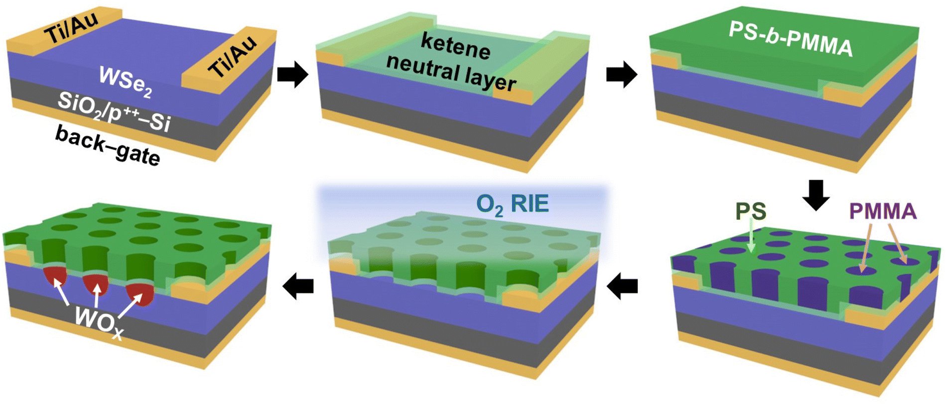 | ||
| Fig. 1 Fabrication of the self-powered WSe2 photodetector with the 3D nanostructured homojunction using the BCP nanolithography process. | ||
Preparation of BCP nanoporous patterns
The PS-b-PMMA (MPS = 57 kg mol−1, MPMMA = 25 kg mol−1, Mw/Mn = 1.07) BCP was purchased from Polymer Source Inc. Meldrum's acid containing cross-linkable PS-r-PMMA random copolymers was synthesized using a previously reported method.42 It consists of styrene (52 mol%), MMA (45 mol%), and Meldrum's acid (3 mol%), and the total number average molecular weight was 24 kg mol−1 (Mw/Mn = 1.13).42 To obtain vertically oriented cylindrical nanopatterns on WSe2 FETs, WSe2 surfaces were neutralized with cross-linkable PS-r-PMMA random copolymers by spin-coating (3000 rpm, 45 s) 0.4 wt% toluene solution. Then, the PS-r-PMMA layer was thermally cross-linked at 230 °C for 1 h in vacuo. To prepare BCP films, 2 wt% toluene solution of PS-b-PMMA was prepared and spin-coated (3000 rpm, 45 s) on the WSe2 substrate possessing a cross-linked neutral layer. Then, the BCP-coated WSe2 FETs were thermally annealed at 210 °C for 24 h. To prepare nanoporous BCP templates, RIE was employed using O2 with an RF power of 90 W at 20 sccm (Cute-1MP, Femto Science) to selectively remove PMMA microdomains and the underlying neutral layers. The etch rates were 0.81, 1.47, and 1.16 nm s−1 for PS, PMMA, and the cross-linked PS-r-PMMA neutral layer, respectively.Characterization
The thicknesses of the cross-linked PS-r-PMMA neutral layers and PS-b-PMMA BCP films were measured using spectroscopic ellipsometry (SE MG-1000, Nano-view Co.) at an incidence angle of 70.2° based on the Cauchy model. An atomic force microscope (AFM, Park Systems NX-10) was used to determine the thickness of the WSe2 flakes and characterize the BCP nanopatterns on the WSe2 surfaces. Phase and Z-height profile data were obtained with non-contact mode settings. A field emission scanning electron microscope (FE-SEM) (JSM-6700F, JEOL) was employed to investigate the nanoporous BCP pattern on the WSe2 flake. The optical properties of the WSe2 flake before and after BCP patterning were characterized using micro-Raman spectroscopy under the back-scattering geometry with a diode-pumped solid-state laser (Omicron) of 532 nm wavelength. The optoelectronic properties were determined using a semiconductor parameter analyzer (Agilent 4155C) connected to a low-vacuum probe station (7.9 mTorr). The optical intensities of LED light sources (Newport) of 530 and 780 nm were calibrated using a power meter (FieldMaxII-TO, Coherent). An optical beam shutter (SHB1T, Thorlabs) connected to a pulse generator (Agilent 33250A) was used to analyze the time-dependent photoresponses of the fabricated photodetectors.Results and discussion
To enhance the optoelectrical properties of the WSe2 photodetector, nanoporous BCP patterns were prepared on the WSe2 surfaces (Fig. 1). First, back-gated ML WSe2 FETs were fabricated by transferring exfoliated WSe2 flakes onto a SiO2 substrate, followed by the deposition of Ti/Au electrodes. Then, cylinder-forming PS-b-PMMA BCP thin films were prepared on the WSe2 surfaces with a film thickness of ∼74 nm. To obtain nano-dot arrays, cylindrical PMMA microdomains need to be oriented perpendicularly to the substrate, and this can be accomplished using the ultrathin layer of the PS-r-PMMA random copolymer that neutralizes the WSe2 surface.42–52 In this study, we employed a cross-linkable PS-r-PMMA random copolymer containing Meldrum's acid, which generates reactive ketenes upon heating and forms a cross-linked neutral layer.42 The BCP was spin-coated on the neutral layer and annealed at 210 °C. As shown in Fig. 2(c), hexagonally packed nano-dot arrays are formed, indicating the vertically oriented PMMA cylinders. To generate nanoporous patterns, the PMMA microdomains were selectively removed using O2 RIE with known etching rates of PS and PMMA (PS: 0.81 nm s−1, PMMA: 1.47 nm s−1). After the complete removal of PMMA and the underlying neutral layer, additional RIE was allowed for a few seconds to oxidize the exposed WSe2, creating nanopatterned WOx embedded on the WSe2 surface. As shown in Fig. 2(e), the average diameter of the nanopore is 28 nm with a domain spacing of 40 nm.53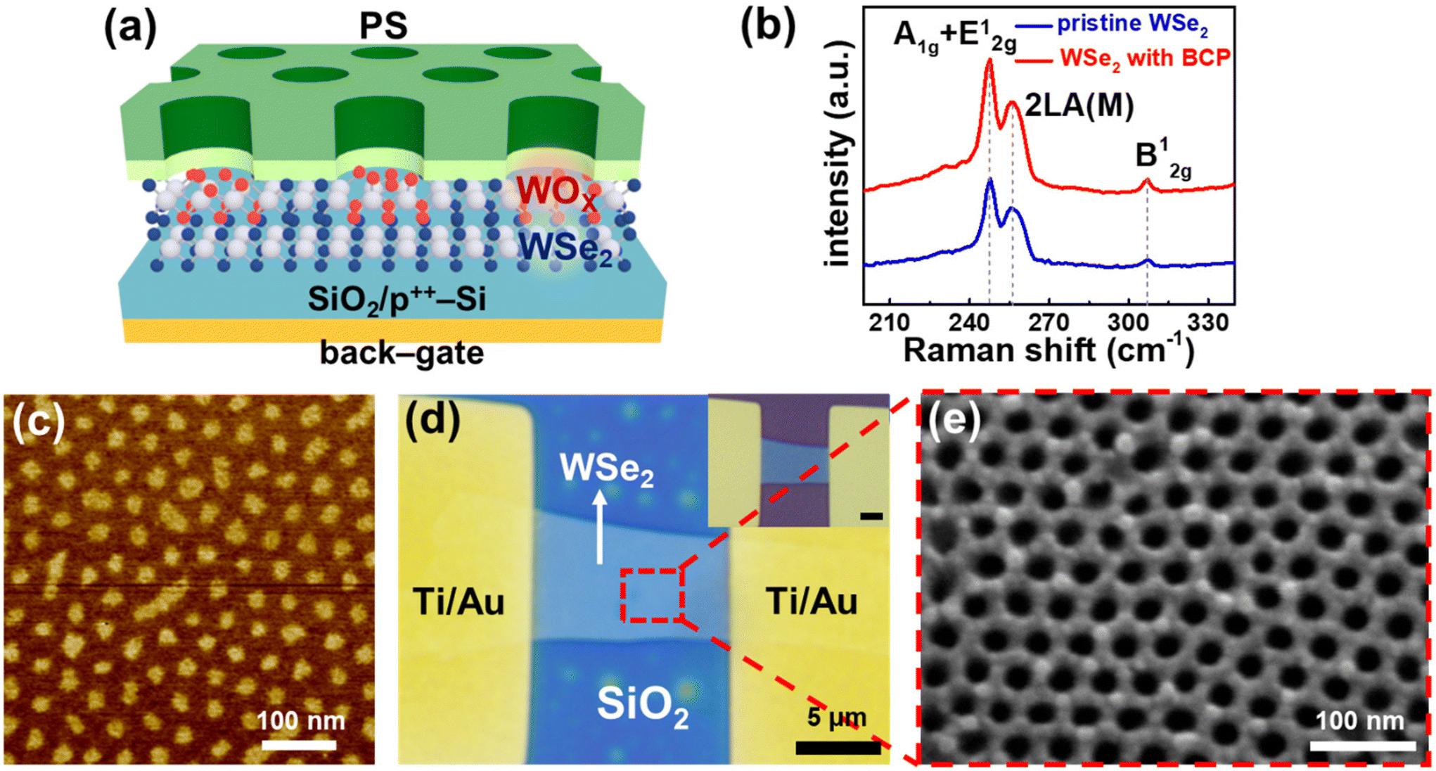 | ||
| Fig. 2 (a) Schematic of the 3D WSe2 homojunction with nanoporous PS. (b) Micro-Raman spectra of the pristine and BCP-patterned WSe2. (c) AFM phase image of cylinder-forming PS-b-PMMA BCP thin films on the WSe2 flake. (d) Optical microscopy of the WSe2 photodetector. (e) SEM images of nanoporous BCP patterns on the WSe2 photodetector. | ||
The oxygen plasma treatment during PMMA removal makes the underlying WSe2 oxidized, forming the structure of WOx/WSe2 (Fig. 2(a)). As WOx with a high work-function makes the neighboring WSe2 electron-deficient, the underlying WSe2 can be p-doped using the charge-transfer process.23 The oxidation of WSe2 has been intensively investigated using laser annealing,54 oxygen plasma,55 UV-ozone treatment,56 and thermal annealing24 under oxygen ambient conditions. Yang et al. effectively constructed seamless WSe2 homojunction diodes by converting the top few layers of WSe2 to WOx (x < 3) via 325 nm laser exposure.54 Moon et al. fabricated an oxidized WSe2 FET with reduced channel resistance and a clean interface using the oxygen plasma treatment.57 The oxidation of WSe2, which is a self-limiting process, is initiated by substituting the Se vacancy with an oxygen atom; this is a spontaneous process with an enthalpy of −4.7 eV.58 Micro-Raman spectroscopy confirms that the crystallinity of the underlying WSe2 is well maintained after BCP patterning (Fig. 2(b)), although the oxidation process may create dangling bonds in the WSe2 layer because the oxidation can proceed in the out-of-plane direction through the intrinsic defects. Fig. 2(d) shows the optical microscopy image of the ML WSe2 photodetector possessing nanoporous BCP patterns. The SEM image of the nanoporous ML WSe2 device indicates that the cylindrical PMMA microdomains are oriented perpendicularly to the WSe2 surface, implying that the proposed single-step BCP nanolithography process is applicable for the post-fabrication process of TMD materials.
The current–voltage (IDS–VDS) characteristics of the nanoporous WSe2 FETs at zero VGS were compared under different illumination conditions as shown in Fig. 3(a) and (b). The low current levels can be attributed to the unwanted interface states and the non-optimization of the device layout. The EHPs were created using 530 and 780 nm wavelengths, generating photocurrents. The increase in the photocurrents was higher for the nanoporous WSe2 FET owing to the formation of 3D built-in electric fields (Fig. 3(c)). In pristine WSe2, no electric fields exist, which is inefficient for collecting the generated EHPs under the exposure of light (Fig. 3c, left). Compared to the pristine one, the formation of layered WOx can help develop 2D electric fields; it is a conventional method to form built-in electric fields (Fig. 3c, middle). In contrast, the nanopatterned BCP architecture can form 3D electric fields, which allows us to collect additional EHPs owing to the expansion of the depletion region (right side of Fig. 3(c)). The photons that were absorbed near and in the depletion region can help generate photocurrents.
 | ||
| Fig. 3 Current–voltage characteristics of the (a) pristine and (b) nanopatterned WSe2 device under different irradiation conditions (dark, and 530 nm and 780 nm wavelengths). (c) WSe2 without a junction (left), WSe2 with a planar junction (middle), and WSe2 with a 3D nanostructured junction (right). (d) Responsivity (R) and (e) external quantum efficiency (EQE) at varying values of VGS. | ||
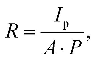
Although the one-atom-thick TMD layer may achieve optimal electrical performance with a high on/off ratio and low power consumption, the lower optical absorption compared to the thick one limits its optoelectronic properties. As an alternative, the ML TMD layer is beneficial for optical absorbance. As the collection efficiency increases with the expansion of the depletion region, the photoresponse performances (responsivity (R) and external quantum efficiency (EQE)) were improved using the positive value of VGS (Fig. 3(d) and (e)) under the illumination of 530 nm wavelength, implying the WOx-induced p-doping of WSe2. Operation in the increased depletion region under the appropriate gate bias caused the formation of the absorber layer, which is extremely sensitive to incoming photons through the channel. The optoelectronic parameters under the bias conditions of VDS = +1 V and VGS = 0 V are shown in Fig. 4(d). The responsivity (R) of the nanoporous WSe2 photodetector was calculated using the following equation:
where h denotes the Planck constant, c denotes the speed of light, and λ denotes the wavelength of the illuminated light. The detectivity (D*) and photo-to-dark current ratio (PDCR) were obtained using the following equations:


where q denotes the electronic charge. The dynamic photoresponse characteristics of WSe2 photodetectors were compared with and without BCP nanopatterns. As shown in Fig. 4(a) and (b), time-dependent photocurrents were measured at varying intensities of 530 nm wavelength. The photocurrents increased with an increase in the light intensity, which indicates the high quality of the WOx/WSe2 structure (Fig. 4(c)). The optoelectronic performances significantly improved after BCP patterning on WSe2 with fast response and decay characteristics. Persistent photoconductivity (PPC) was not observed, indicating that BCP patterning induced nominal defects in WSe2. The self-powered photodetection mechanism of the nanoporous WSe2 photodetector illustrated in Fig. 5(a) was demonstrated, where high photocurrents were obtained after BCP patterning (Fig. 5(b)). The negligible photocurrent obtained from the pristine WSe2 photodetector can be attributed to the non-ideal Ohmic contact with WSe2 caused by Fermi-level pinning. The performance of the self-powered WSe2 photodetector is illustrated in Fig. 5(c). Among the different methods to form built-in electric fields, including Schottky contacts, the p–n homojunction, and the p–n heterojunction, the p–n homojunction can be ideal because it nominally affects the absorber layer. Self-powered photodetectors can be miniaturized because they do not require external power sources.

 | ||
| Fig. 4 Time-dependent photocurrent characteristics of the (a) pristine and (b) nanopatterned WSe2 photodetector at varying optical intensities (530 nm wavelength). (c) Photocurrent at different optical intensities. (d) Optoelectronic parameters under the bias conditions of VDS = +1 V and VGS = 0 V considering the exposure of 530 nm with a light power density of 1.8 mW cm−2. | ||
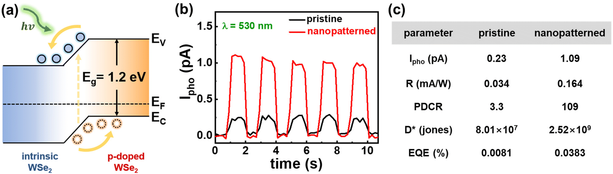 | ||
| Fig. 5 (a) Mechanism of the self-powered WSe2 photodetector. (b) Time-dependent photocurrent characteristics. (c) Optoelectronic performances of the pristine and nanopatterned WSe2. | ||
Conclusion
A 3D homojunction was demonstrated in WSe2 using a one-step BCP nanolithography process, enabling an effective collection of EHPs. The oxygen plasma used to remove PMMA cylindrical microdomains in PS-b-PMMA thin films oxidized the underlying WSe2, forming a 3D WOx/WSe2 structure. The current–voltage output and transfer characteristics based on the fabricated WOx/WSe2 FET were obtained under dark and different illumination conditions, confirming the formation of built-in electric fields. The optoelectronic performances, including responsivity, PDCR, detectivity, and EQE, were significantly improved owing to the introduction of the multi-dimensional homojunction structure. There was no PPC at varying light power, implying a high-quality interface. Self-powered photodetection, which can operate without an external power source, was demonstrated with excellent static and dynamic photosensing performance. This study can provide a pathway for the development of high-performance stand-alone photodetectors based on the multidimensional device architecture.Conflicts of interest
There are no conflicts to declare.Acknowledgements
This work was supported by a National Research Foundation of Korea (NRF) grant funded by the Korean government (MSIT) (No. 2020M3H4A3081799 and 2022R1A4A1020543) and the K-Sensor Development Program (No. RS-2022-00154729), funded by the Ministry of Trade, Industry and Energy (MOTIE, Korea).References
- F. Yan, Z. Wei, X. Wei, Q. Lv, W. Zhu and K. Wang, Small Methods, 2018, 2, 1700349 CrossRef
.
- C. Liu, J. Guo, L. Yu, J. Li, M. Zhang, H. Li, Y. Shi and D. Dai, Light: Sci. Appl., 2021, 10, 123 CrossRef CAS PubMed
- C. Xie, C. Mak, X. Tao and F. Yan, Adv. Funct. Mater., 2017, 27, 1603886 CrossRef
- M. Long, P. Wang, H. Fang and W. Hu, Adv. Funct. Mater., 2019, 29, 1803807 CrossRef
- T. Tan, X. Jiang, C. Wang, B. Yao and H. Zhang, Adv. Sci., 2020, 7, 2000058 CrossRef CAS PubMed
- K. S. Novoselov, A. Mishchenko, A. Carvalho and A. H. Castro Neto, Science, 2016, 353, aac9439 CrossRef CAS PubMed
- F. Wang, K. Pei, Y. Li, H. Li and T. Zhai, Adv. Mater., 2021, 33, 2005303 CrossRef CAS PubMed
- S. Das and J. Appenzeller, Appl. Phys. Lett., 2013, 103, 103501 CrossRef
- Z. Jin, X. Li, J. T. Mullen and K. W. Kim, Phys. Rev. B: Condens. Matter Mater. Phys., 2014, 90, 045422 CrossRef CAS
- L. Yu, A. Zubair, E. J. Santos, X. Zhang, Y. Lin, Y. Zhang and T. Palacios, Nano Lett., 2015, 15, 4928–4934 CrossRef CAS PubMed
- L. Ye, P. Wang, W. Luo, F. Gong, L. Liao, T. Liu, L. Tong, J. Zang, J. Xu and W. Hu, Nano Energy, 2017, 37, 53–60 CrossRef CAS
- J. Chen, Q. Wang, Y. Sheng, G. Cao, P. Yang, Y. Shan, F. Liao, Z. Muhammad, W. Bao and L. Hu, ACS Appl. Mater. Interfaces, 2019, 11, 43330–43336 CrossRef CAS PubMed
- H. Xue, Y. Wang, Y. Dai, W. Kim, H. Jussila, M. Qi, J. Susoma, Z. Ren, Q. Dai and J. Zhao, Adv. Funct. Mater., 2018, 28, 1804388 CrossRef
- M. H. Jeong, H. S. Ra, S. H. Lee, D. H. Kwak, J. Ahn, W. S. Yun, J. Lee, W. S. Chae, D. K. Hwang and J. S. Lee, Adv. Mater., 2022, 34, 2108412 CrossRef CAS PubMed
- J. Lu, A. Carvalho, H. Liu, S. X. Lim, A. H. Castro Neto and C. H. Sow, Angew. Chem., 2016, 128, 12124–12128 CrossRef
- P. Luo, F. Zhuge, Q. Zhang, Y. Chen, L. Lv, Y. Huang, H. Li and T. Zhai, Nanoscale Horiz., 2019, 4, 26–51 RSC
- X. Yu, S. Zhang, H. Zeng and Q. J. Wang, Nano Energy, 2016, 25, 34–41 CrossRef CAS
- Z.-Q. Xu, Y. Zhang, Z. Wang, Y. Shen, W. Huang, X. Xia, W. Yu, Y. Xue, L. Sun and C. Zheng, 2D Mater., 2016, 3, 041001 CrossRef
- J. Wang, J. Han, X. Chen and X. Wang, InfoMat, 2019, 1, 33–53 CrossRef CAS
- J. Huang, T. B. Hoang and M. H. Mikkelsen, Sci. Rep., 2016, 6, 22414 CrossRef CAS PubMed
- T. Mueller and E. Malic, npj 2D Mater. Appl., 2018, 2, 29 CrossRef
- J. Meyer, S. Hamwi, M. Kröger, W. Kowalsky, T. Riedl and A. Kahn, Adv. Mater., 2012, 24, 5408–5427 CrossRef CAS PubMed
- M. Yamamoto, S. Dutta, S. Aikawa, S. Nakaharai, K. Wakabayashi, M. S. Fuhrer, K. Ueno and K. Tsukagoshi, Nano Lett., 2015, 15, 2067–2073 CrossRef CAS PubMed
- Y. Liu, C. Tan, H. Chou, A. Nayak, D. Wu, R. Ghosh, H.-Y. Chang, Y. Hao, X. Wang and J.-S. Kim, Nano Lett., 2015, 15, 4979–4984 CrossRef CAS PubMed
- Y. C. Lin, B. M. Bersch, R. Addou, K. Xu, Q. Wang, C. M. Smyth, B. Jariwala, R. C. Walker, S. K. Fullerton-Shirey and M. J. Kim, Adv. Mater. Interfaces, 2020, 7, 2000422 CrossRef CAS
- M. Yamamoto, S. Nakaharai, K. Ueno and K. Tsukagoshi, Nano Lett., 2016, 16, 2720–2727 CrossRef CAS PubMed
- H. Park, J. Lee, G. Han, A. AlMutairi, Y.-H. Kim, J. Lee, Y.-M. Kim, Y. J. Kim, Y. Yoon and S. Kim, Commun. Mater., 2021, 2, 94 CrossRef CAS
- H. Xue, Y. Dai, W. Kim, Y. Wang, X. Bai, M. Qi, K. Halonen, H. Lipsanen and Z. Sun, Nanoscale, 2019, 11, 3240–3247 RSC
- G. Nazir, M. F. Khan, I. Akhtar, K. Akbar, P. Gautam, H. Noh, Y. Seo, S.-H. Chun and J. Eom, RSC Adv., 2017, 7, 16890–16900 RSC
- C. Chen, H. Qiao, S. Lin, C. M. Luk, Y. Liu, Z. Xu, J. Song, Y. Xue, D. Li and J. Yuan, Sci. Rep., 2015, 5, 11830 CrossRef PubMed
- S. Qiao, R. Cong, J. Liu, B. Liang, G. Fu, W. Yu, K. Ren, S. Wang and C. Pan, J. Mater. Chem. C, 2018, 6, 3233–3239 RSC
- J. Bang, U. Jeong, D. Y. Ryu, T. P. Russell and C. J. Hawker, Adv. Mater., 2009, 21, 4769–4792 CrossRef CAS PubMed
- L. Leibler, Macromolecules, 1980, 13, 1602–1617 CrossRef CAS
- F. S. Bates and G. H. Fredrickson, Annu. Rev. Phys. Chem., 1990, 41, 525–557 CrossRef CAS PubMed
- R. A. Segalman, Mater. Sci. Eng., R, 2005, 48, 191–226 CrossRef
- C. J. Hawker and T. P. Russell, MRS Bull., 2005, 30, 952–966 CrossRef CAS
- T. P. Russell, R. P. Hjelm Jr. and P. A. Seeger, Macromolecules, 1990, 23, 890–893 CrossRef CAS
- T. Xu, H.-C. Kim, J. DeRouchey, C. Seney, C. Levesque, P. Martin, C. Stafford and T. Russell, Polymer, 2001, 42, 9091–9095 CrossRef CAS
- A. Menelle, T. Russell, S. Anastasiadis, S. Satija and C. Majkrzak, Phys. Rev. Lett., 1992, 68, 67 CrossRef CAS PubMed
- H. C. Kim and T. P. Russell, J. Polym. Sci., Part B: Polym. Phys., 2001, 39, 663–668 CrossRef CAS
- T. P. Russell and Y. Chai, Macromolecules, 2017, 50, 4597–4609 CrossRef CAS
- H. Jung, F. A. Leibfarth, S. Woo, S. Lee, M. Kang, B. Moon, C. J. Hawker and J. Bang, Adv. Funct. Mater., 2013, 23, 1597–1602 CrossRef CAS
- D. Y. Ryu, K. Shin, E. Drockenmuller, C. J. Hawker and T. P. Russell, Science, 2005, 308, 236–239 CrossRef CAS PubMed
- D. Y. Ryu, J.-Y. Wang, K. A. Lavery, E. Drockenmuller, S. K. Satija, C. J. Hawker and T. P. Russell, Macromolecules, 2007, 40, 4296–4300 CrossRef CAS
- H. Jung, D. Hwang, E. Kim, B.-J. Kim, W. B. Lee, J. E. Poelma, J. Kim, C. J. Hawker, J. Huh and D. Y. Ryu, ACS Nano, 2011, 5, 6164–6173 CrossRef CAS PubMed
- H. S. Wang, K. H. Kim and J. Bang, Macromol. Rapid. Commun., 2019, 40, 1800728 CrossRef PubMed
- S. H. Kim, M. J. Misner and T. P. Russell, Adv. Mater., 2008, 20, 4851–4856 CrossRef CAS
- P. Mansky, Y. Liu, E. Huang, T. Russell and C. Hawker, Science, 1997, 275, 1458–1460 CrossRef CAS
- E. Huang, L. Rockford, T. Russell and C. Hawker, Nature, 1998, 395, 757–758 CrossRef CAS
- S. Ham, C. Shin, E. Kim, D. Y. Ryu, U. Jeong, T. P. Russell and C. J. Hawker, Macromolecules, 2008, 41, 6431–6437 CrossRef CAS
- S. Park, J.-Y. Wang, B. Kim, J. Xu and T. P. Russell, ACS Nano, 2008, 2, 766–772 CrossRef CAS PubMed
- E. Huang, S. Pruzinsky, T. Russell, J. Mays and C. Hawker, Macromolecules, 1999, 32, 5299–5303 CrossRef CAS
- H. S. Wang, A. Khan, Y. Choe, J. Huh and J. Bang, Macromolecules, 2017, 50, 5025–5032 CrossRef CAS
- S. Yang, G. Lee, J. Kim, S. Yang, C.-H. Lee and J. Kim, J. Mater. Chem. C, 2020, 8, 8393–8398 RSC
- Z. Li, S. Yang, R. Dhall, E. Kosmowska, H. Shi, I. Chatzakis and S. B. Cronin, ACS Nano, 2016, 10, 6836–6842 CrossRef CAS PubMed
- D. Lee, Y. Choi, J. Kim and J. Kim, ACS Nano, 2022, 16, 8484–8492 CrossRef CAS PubMed
- I. Moon, S. Lee, M. Lee, C. Kim, D. Seol, Y. Kim, K. H. Kim, G. Y. Yeom, J. T. Teherani and J. Hone, Nanoscale, 2019, 11, 17368–17375 RSC
- J. Lu, A. Carvalho, X. K. Chan, H. Liu, B. Liu, E. S. Tok, K. P. Loh, A. H. Castro Neto and C. H. Sow, Nano Lett., 2015, 15, 3524–3532 CrossRef CAS PubMed
- D.-H. Kwak, P. Ramasamy, Y.-S. Lee, M.-H. Jeong and J.-S. Lee, ACS Appl. Mater. Interfaces, 2019, 11, 29041–29046 CrossRef CAS PubMed
Footnote |
| † These authors contributed equally to this work. |
| This journal is © The Royal Society of Chemistry 2023 |