
Spatial distribution of triplet excitons formed from charge transfer states at the donor/acceptor interface†
Seiichiro
Izawa
 *abc,
Masahiro
Morimoto
*d,
Shigeki
Naka
d and
Masahiro
Hiramoto
ab
*abc,
Masahiro
Morimoto
*d,
Shigeki
Naka
d and
Masahiro
Hiramoto
ab
aInstitute for Molecular Science, 5-1 Higashiyama, Myodaiji, Okazaki 444-8787, Aichi, Japan. E-mail: izawa@ims.ac.jp
bThe Graduate University for Advanced Studies (SOKENDAI), 5-1 Higashiyama, Myodaiji, Okazaki, Aichi 444-8787, Japan
cPrecursory Research for Embryonic Science and Technology (PRESTO), Japan Science and Technology Agency (JST), 4-1-8 Honcho, Kawaguchi, Saitama 332-0012, Japan
dAcademic Assembly Faculty of Engineering, University of Toyama, 3190 Gofuku, Toyama 930-8555, Japan. E-mail: morimoto@eng.u-toyama.ac.jp
First published on 31st May 2022
Abstract
Triplet exciton formation at an organic semiconductor interface plays a crucial role in photophysical processes in electronic devices, such as organic light-emitting diodes (OLEDs) and organic photovoltaics, and in optical functions, such as photon upconversion (PUC) based on triplet–triplet annihilation (TTA), which produces a photon with high energy combining two photons with low energy. Herein, we report the spatial distribution of the triplet exciton generated after charge recombination at the organic semiconductor interface. The triplet exciton distribution is assessed by examining the variation in TTA emission when the triplet quencher is doped near the interface in the OLED and PUC systems. The obtained result indicates that 90% of the triplet excitons are confined to less than 10 nm from the donor/acceptor interface, where charge recombination occurs and a charge transfer state forms, which is a precursor of the triplet exciton. The confinement of triplet excitons leads to efficient TTA emission, whose efficiency is triplet concentration-dependent, in OLED and PUC systems utilizing the mechanism of interfacial triplet formation.
 Seiichiro Izawa | Seiichiro Izawa has been working as an assistant professor at the Institute for Molecular Science, Japan, since 2016. He received his PhD from the University of Tokyo in 2015 and worked at RIKEN in Japan and University of California, Santa Barbara as a postdoctoral fellow from Japan Society for the Promotion of Science. His research interests include controlling optoelectronic properties at the organic semiconductor interface for application of organic photovoltaics, light-emitting diodes and photon upconversion. |
Introduction
The spin statistics rule states that 75% of the excitons formed after free charge recombination are spin triplets.1 The triplet excited state is generally dark because the transition to the ground state is spin-forbidden. Therefore, ensuring that triplet excitons emit light is an important research target for realizing efficient organic light-emitting diodes (OLEDs). This subject is solved by developing thermally activated delayed fluorescent materials that convert triplet excitons to singlets2 and phosphorescent materials that have large spin–orbit coupling, which enables emission from a triplet state.3 Recently, triplet excitons have been recognized for their crucial role in the charge recombination of organic photovoltaics (OPVs).4,5 A triplet exciton forms after bimolecular charge recombination through an intermediate charge transfer (CT) state at the donor/acceptor (D/A) interface. The formation of the triplet exciton after charge recombination is supposed to be the main cause of non-radiative recombination loss,5 which is the main problem that causes a large energy loss in the open-circuit voltage in OPVs, leading to a lower power conversion efficiency of OPVs than that of perovskite, crystalline-silicon, and GaAs PVs.6,7 To enhance the performance of organic electronic devices, such as OLEDs and OPVs, it is important to clearly define the behavior of triplet exciton formation after charge recombination.Recently, we have leveraged the triplet exciton formation resulting in the CT state after charge recombination at the D/A interface to construct an efficient photon upconversion (PUC) system in the solid state.8 PUC is a process in which a material increases the energy of the incident photons, resulting in the emission of photons with higher energies.9 PUC in the solid state has attracted much attention because of its potential applications in solar cells, photocatalysis, and photodynamic therapy in living organisms.10,11 However, the external quantum efficiency (EQE) of a conventional PUC system based on intersystem crossing, namely triplet formation by the heavy-atom effect in a molecule, is as low as 0.024% in the solid state.12 The PUC emission in our system occurs after triplet–triplet annihilation (TTA) that originates from triplet formation through photo-excited singlet separation and free charge recombination at the interface of the D/A bilayer film. As a result, a solid-state PUC from the near-infrared to the visible light region on flexible organic thin films without using heavy atoms is achieved with an external efficiency that is two orders of magnitude higher than those demonstrated in conventional systems based on intersystem crossing in a sensitizer molecule containing a heavy atom.8,12 The concept of PUC at the D/A interface has been expanded to develop efficient OLEDs operated at extremely small driving voltages.13 Electroluminescence (EL) emission in the OLED occurs through the formation of a charge transfer state with a spin triplet (CT3) originating from injected charges, followed by TTA.13–15 This is a current-excited UC process in the OLED device, while PUC is a photo-excited process. The OLED was realized to emit light with a wavelength of 608 nm (2.04 eV) at a luminance of 177 cd m−2 and is operable with a 1.5 V battery, which, to the best of our knowledge, is the lowest OLED operating voltage reported to date.13 In the PUC and OLED devices, we suppose that the motility of the triplet excitons formed from the CT state plays a crucial role in efficient TTA emission. To enhance the efficiency of such photophysical processes, the real spatial distribution of triplet excitons near the D/A interface should be clarified.
In this study, the spatial distribution of triplet excitons formed from the CT state at the D/A interface was elaborated on by analyzing the EL emission in an OLED device and PUC emission on a bilayer thin film. A phosphorescent material was doped near the D/A interface, which served as a trap for the triplet excitons. The trap dopant quenched the TTA emission released from the host material and emitted phosphorescence instead. The relationship between the thickness of the doped layer and the variation in the emission intensities directly demonstrates the spatial distribution of the triplet excitons near the D/A interface.
Results and discussion
In this study, we utilized a D/A-type OLED device based on rubrene and N,N′-di-n-octyl-3,4,9,10-perylenetetracarboxylic diimide (PTCDI) (Fig. 1a), which has been reported as an efficient OLED with an extremely low driving voltage in the literature,13 to investigate the spatial distribution of the triplet excitons near the D/A interface. The emission scheme of the OLED, which is illustrated in Fig. 1b, is described as follows: CT3 forms after the charge recombination of injected charges at the D/A interface. Then, the energy of the CT3 state is transferred to T1 of rubrene. Later, the fluorescence of rubrene is observed through TTA. In this study, copper(II) phthalocyanine (CuPc) was doped inside the rubrene layer as the triplet trap. CuPc emits phosphorescence at approximately 1100 nm (1.12 eV),16,17 which is slightly less than the T1 energy of rubrene (1.14 eV).18 Therefore, Dexter energy transfer from rubrene T1 to CuPc T1 is possible. The PUC system utilizes 3,9-bis(2-methylene-((3-(1,1-dicyanomethylene)-6,7-dichloro)-indanone))-5,5,11,11-tetrakis(4-hexylphenyl)-dithieno[2,3-d:2′,3′-d′]-s-indaceno[1,2-b:5,6-b′]dithiophene (ITIC-Cl; Fig. 1a), which is a famous non-fullerene acceptor in the OPV field,19 instead of PTCDI in the OLED device. ITIC-Cl can absorb near infrared (NIR) light, and the rubrene/ITIC-Cl bilayer can efficiently convert NIR light to yellow light with a high EQE of 1.29%.8 The mechanism of the PUC is based on the same CT-TTA emission as that used in the OLED device. Free charges in the PUC system are generated through photoexcitation in ITIC-Cl and charge separation at the D/A interface.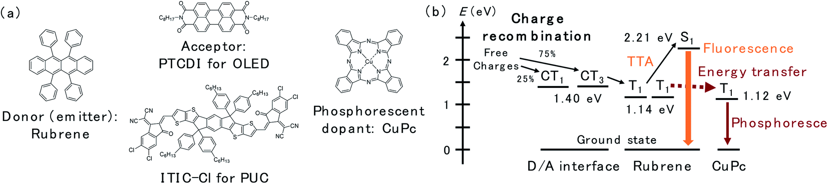 | ||
| Fig. 1 (a) Chemical structures of rubrene, PTCDI, ITIC-Cl and CuPc. (b) The energy levels of excited states and schematic of the energy transfer inside the device. | ||
The structure of the OLED device is presented in Fig. 2a. The triplet trap: CuPc was doped in the rubrene layer near the D/A interface. The doping concentration of CuPc was set to 1 vol% because the efficiency of the CuPc emission reached a maximum under this condition.16 Atomic force microscopy images for undoped and CuPc-doped rubrene films are presented in Fig. S1.† The surfaces of both films were very smooth, excluding the possibility of the morphological change by the CuPc-doping. The thicknesses of the CuPc-doped layers were 5, 10, 25, 50, and 100 nm, while the total thickness of the doped layer plus the pristine rubrene layer was kept constant at 110 nm because we wanted to compare the doping effect near the D/A interface without changing the device conditions such as an optical interference effect. 110 nm is sufficiently thicker than the typical triplet exciton diffusion length in amorphous films of organic semiconductors.20Fig. 2b shows the luminance (L)–current density (J) characteristics of the prepared OLED devices. Luminance is based on the spectral sensitivity of the human eye; therefore, it is insensitive to NIR emission released from CuPc. The luminance value reflects only the emission intensity from the fluorescence of rubrene in the visible region. The luminance value drastically decreases with an increasing thickness of the CuPc-doped layer. This is because CuPc traps triplet excitons in the rubrene layer and quenches TTA emission from the rubrene host. The luminance value does not decrease any further with CuPc-doped layer thickness higher than 25 nm. The same trend was observed in the spectral intensity of the rubrene emission presented in Fig. 2c. The rubrene emission at 565 nm decreases with an increase in the CuPc-doped layer thickness up to 25 nm. These results suggest that triplet excitons were mainly distributed in the region below 25 nm near the D/A interface. Instead of quenching the TTA emission from rubrene by CuPc doping, the CuPc emission appears at 1100 nm in Fig. 2d. This result indicates that triplet energy is transferred from rubrene to CuPc. The intensity of CuPc emission is increased for thicker devices compared to a device with a 5 nm doped layer, despite the CuPc emission being very small. The reason for the weak CuPc emission is its very low EQE of EL, reported as ∼10−3%.16 The change in the rubrene emission intensity owing to CuPc doping near the D/A interface was also investigated in the rubrene/ITIC-Cl PUC system.8 The device structure and PUC emission excited with 750 nm LED light are presented in Fig. S2.† As in the case of EL emission, PUC emission from rubrene is gradually quenched by increasing the thickness of the CuPc-doped layer up to 25 nm. This result indicates that triplet excitons generated by light irradiation in the PUC system are distributed in the region below 25 nm near the D/A interface, similar to the triplet excitons generated by the injected current in the OLED device. The triplet exciton distribution is further investigated in OLED devices because the excitation light source in the PUC system disturbs the detection of CuPc emission.
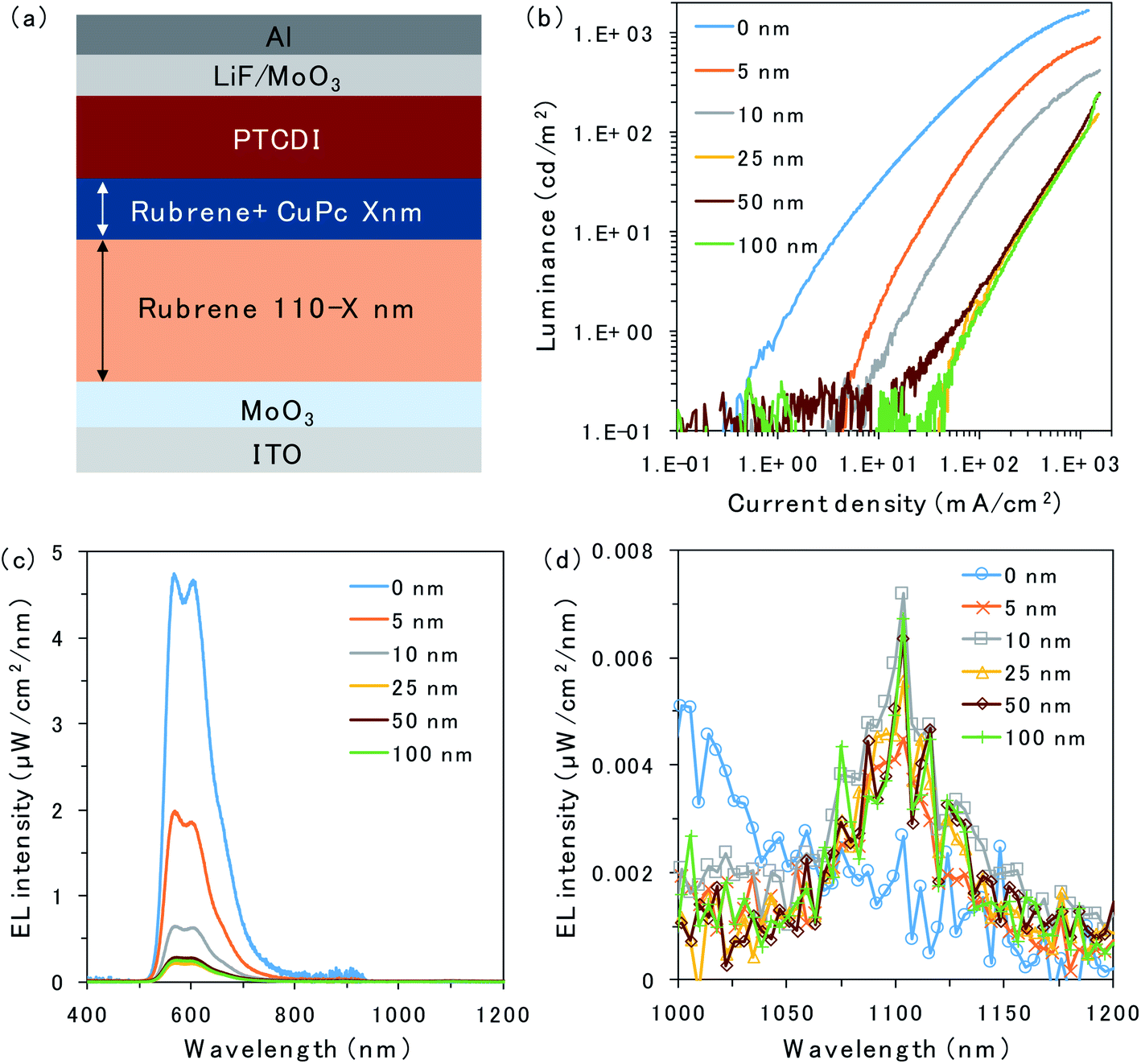 | ||
| Fig. 2 (a) Schematic of the device with the CuPc-doped rubrene layer at the D/A interface. (b) L–J curves and (c and d) EL emission spectra with a constant current flow (1000 mA cm−2) for the devices with 0 nm (blue), 5 nm (orange), 10 nm (grey), 25 nm (yellow), 50 nm (brown), and 100 nm (green) of CuPc-doped rubrene layers at the D/A interface. | ||
To further investigate triplet exciton diffusion after charge recombination, a pristine rubrene interlayer was inserted between the 50 nm CuPc-doped layer and D/A interface, as shown in Fig. 3a. When the CuPc-doped layer was 10 nm away from the D/A interface, the intensity of the rubrene emission was small, as can be observed in Fig. 3b. Moreover, a small emission peak from CuPc at 1100 nm is observed in Fig. 3c. The rubrene emission recovered in proportion to the distance of the CuPc-doped layer from the interface. The rubrene emission in the device with the CuPc-doped layer 50 nm away from the interface changes only slightly compared to the undoped device. CuPc emission is not observed in the device with a CuPc-doped rubrene layer 50 nm away from the D/A interface. These results indicate that the quenching effect of the TTA emission of the rubrene host by CuPc is limited if it is away from the interface, and the triplet exciton does not exist in the region 50 nm away from the D/A interface.
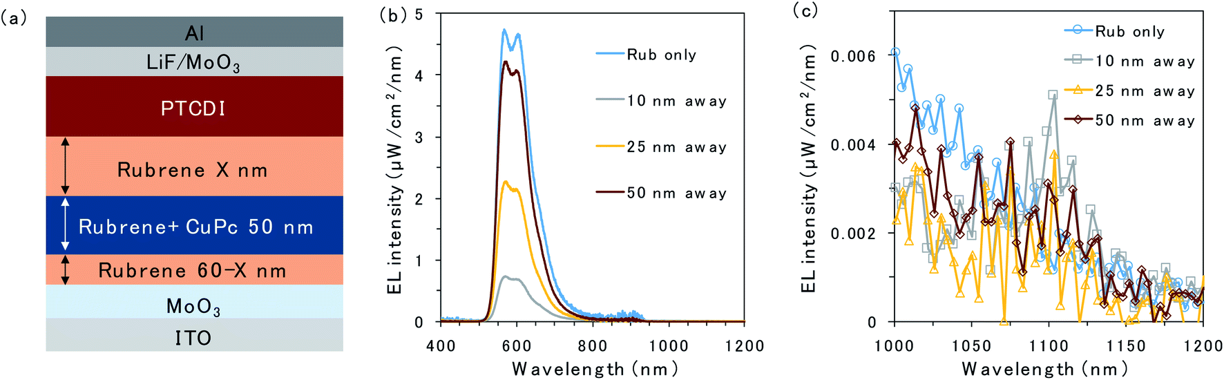 | ||
| Fig. 3 (a) Schematic of the device with 50 nm of a CuPc-doped rubrene layer away from the D/A interface. (b and c) EL emission spectra with a constant current flow (1000 mA cm−2) for the devices without CuPc doping (blue) and with 50 nm of a CuPc-doped rubrene layer away from the D/A interface. The thicknesses of rubrene interlayers at the D/A interface are 10 nm (grey), 25 nm (yellow), and 50 nm (brown). | ||
To clarify the emission mechanism of the CuPc-doped OLED, transient EL decay was measured using a handmade system composed of a silicon photodiode and transimpedance amplifier (Fig. 4). A square voltage waveform at 100 Hz produced by a function generator was applied to the devices. The decay curve mainly reflects the lifetime of the rubrene emission because the CuPc emission is too weak to affect it. The decay curves detected through the NIR cut filter to eliminate CuPc emission are presented in Fig. S3,† depicting curves similar to those presented in Fig. 4. However, the main discussion focuses on the curves measured without the filter to enhance the signal-to-noise ratio. The EL decay curves of the undoped rubrene/PTCDI device and the device with a CuPc-doped rubrene layer 50 nm away from the D/A interface exhibit only one decay component, slow decay, with EL lifetimes of 3.6 and 3.3 μs, respectively. The slow decay is associated with emission resulting from TTA occurring through triplet exciton diffusion. The decay curves of the two devices are almost identical because CuPc is silent for TTA if it exists sufficiently far from the D/A interface. In contrast, the EL decay curve of the device with 25 nm of the CuPc-doped rubrene layer at the D/A interface exhibits two decay components: prompt decay, with EL lifetimes less than 0.1 μs (which is the detection limit of the instrument), and slow decay, with EL lifetimes of 3.4 μs. The slow decay is attributed to TTA emission, whereas the prompt decay is associated with rubrene emission due to the direct excitation of the S1 state by injected charges. The amplitude of the fitted exponential reveals that 90% and 10% of the decay are attributed to direct emission by S1 excitons and TTA, respectively. The results indicate that CuPc near the D/A interface strongly quenches the TTA process.
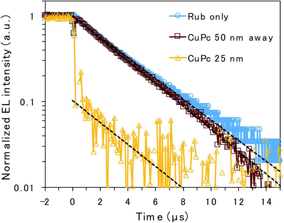 | ||
| Fig. 4 EL decay for the device without CuPc doping (blue circle), with 50 nm of a CuPc-doped rubrene layer at 50 nm away from the D/A interface (brown square), and with 25 nm of a CuPc-doped layer at the D/A interface (yellow triangle). Voltages of 4.6, 6.0, and 11 V were applied to each device. Curves were fitted to the EL decay using single exponential functions (broken lines). | ||
The energy transfer pathway for the CuPc emission is illustrated in Fig. 1b. We assume that the CuPc emission originates from the Dexter energy transfer of triplet excitons from rubrene to CuPc. Two other possible pathways forming the CuPc triplet, namely, the energy transfer from CT3 to T1 of CuPc and that from S1 of rubrene to S1 of CuPc and intersystem crossing to T1 in the CuPc molecule, are excluded for the following reasons. Triplet exciton diffusion is based on Dexter energy transfer, thus requiring a wave function overlap between the two molecules, which means that it can only occur between neighboring molecules.20 Long-range diffusion of T1 of CuPc in a 1% doped film is impossible because CuPc molecules do not contact each other in the diluted films. Consequently, CuPc emission is observed even 10 nm away from the interface, which excluded the possibility of the first pathway, namely energy transfer from CT3 to T1 of CuPc, because triplet exciton diffusion between CuPc molecules is impossible. The second possibility is that Förster resonance energy transfer (FRET) between singlet excitons is typically in the long range because it is based on dipole–dipole coupling.20 To confirm the FRET length in the rubrene/PTCDI OLED system, we inserted a rubrene layer with an emissive dopant, namely, tetraphenyldibenzoperiflanthene (DBP), away from the interface (Fig. S4a†). The emission spectra of the OLED are presented in Fig. S4b.† The DBP emission at 610 and 665 nm are still observed in the device with the DBP located 100 nm away from the interface, indicating that FRET from rubrene to the energy acceptor occurs even if they are 100 nm apart. The CuPc emission disappears at 50 nm from the interface, excluding the possibility of FRET from S1 of rubrene to S1 of CuPc. Accordingly, the decrease in rubrene emission and emergence of CuPc emission originate from the triplet energy transfer from rubrene to CuPc, and the change in those emission intensities reflects the spatial distribution of the triplet exciton in rubrene molecules formed after charge recombination.
The spatial distribution of triplet excitons is plotted in Fig. 5a. The relative triplet density was calculated from the EL intensity change of TTA emission released from rubrene when the CuPc-doped layer was inserted at the D/A interface (Fig. 2c and S5†) instead of CuPc emission because the CuPc emission presented in Fig. 2d is too weak to be discussed quantitatively. The reduction in the EL intensity obtained by inserting the CuPc-doped thin layer is assumed to be quenched by CuPc in the doped region. The relative triplet density was obtained by comparing the EL intensities of the device with 0 and 25 nm CuPc-doped layers, assuming that the entire triplet was quenched when the 25 nm CuPc doped layer was inserted. The reduction in the triplet density as the distance from the D/A interface increases is fitted by an exponential decay function. The triplet exciton diffusion length, which is defined as the density that becomes 1/e, is 4.4 nm. The spatial distribution of triplet excitons in the ITIC-Cl/rubrene PUC system, calculated based on the intensity change of PUC emission from rubrene in Fig. S2,† is plotted in Fig. 5a. The plots regarding the EL and PUC systems overlap well, indicating that the behavior of triplet excitons does not change if it is generated by current injection from the electrode or light excitation. Macroscopic long-range triplet exciton diffusion at the micrometer scale has been reported in a rubrene single crystal.21 However, the evaporated rubrene thin films utilized in this study have an amorphous structure, leading to a shorter diffusion length. Note that most triplet excitons are consumed by TTA in the rubrene thin film because of its high TTA efficiency, namely, 31%,22 when the maximum efficiency of TTA, which is a two-to-one photon conversion process, is defined as 50%, instead of non-radiative decay to the ground state. The fitted exponential decay function reveals that 69% and 90% of the triplet excitons are confined to regions less than 5 nm and 10 nm from the D/A interface, respectively.
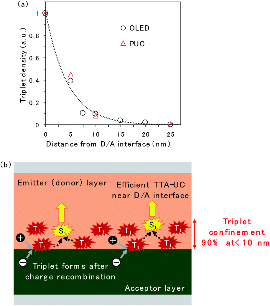 | ||
| Fig. 5 (a) Relative triplet density as a function of distance from the D/A interface. The relative triplet density was calculated according to the intensity change of EL and PUC emission from rubrene when a CuPc-doped layer was inserted at the D/A interface. The black circle represents triplet density in the rubrene/PTCDI OLED device, while the red triangle represents triplet density in the rubrene/ITIC-Cl PUC system. The broken line denotes fitting done using the single exponential regarding the OLED device. (b) Schematic of triplet exciton accumulation after charge recombination near the D/A interface. | ||
A schematic of the TTA emission near the D/A interface is presented in Fig. 5b. The triplet exciton is confined near the D/A interface because it forms at the D/A interface, which has a two-dimensional flat structure. This is one of the reasons why efficient TTA emission could be realized in the OLED and PUC systems utilizing triplet formation through the CT state at the D/A interface. In particular, the PUC at the D/A interface has realized an EQE value two orders of magnitude higher at a smaller excitation light intensity than the conventional PUC system where the triplet exciton forms in a sensitizer molecule, which is dispersed in the entire film, by intersystem crossing.8,11,12 The triplet exciton distribution in the conventional PUC system can be determined using the typical absorption coefficient of organic semiconductor films, which is 105 cm−1,23 meaning that 90% of the photons are absorbed in the films with a thickness of 100 nm. 90% of the triplet excitons are confined to less than 10 nm from the D/A interface in our interfacial PUC system, meaning that the triplet density is ten times larger when it is formed at the interface than when it is randomly formed in the entire film by simple absorption and intersystem crossing. Furthermore, the sensitizer molecules in the conventional PUC system are generally dispersed in a polymer matrix approximately a thousand times to prevent the aggregation of the sensitizer, causing non-radiative triplet recombination,12,24 which leads to a much smaller triplet density in the films. Accordingly, our interfacial PUC system achieves a small saturated excited light intensity, where bimolecular TTA becomes the main decay channel, in the order of several tens of mW cm−2,8 which is ten to thousand times smaller than that of the typical PUC system in the solid state.12,24,25
Conclusions
In summary, we have clarified the spatial distribution of triplet excitons formed from the CT state at the rubrene/acceptor interface in an OLED device and PUC system by analyzing the emission change originating from the rubrene host with CuPc triplet trap molecules. The TTA emission of rubrene was quenched and CuPc emission appeared when CuPc was doped in the region near the D/A interface. The triplet density calculated from the emission change indicates that 90% of the triplet excitons are confined to less than 10 nm from the D/A interface. The confinement is an advantage of triplet generation from the CT state at the D/A interface, which has a two-dimensional flat structure and allows for efficient TTA, whose efficiency is triplet concentration dependent in OLED and PUC systems.Author contributions
S. I. and M. M. conceived the idea, directed the project, and wrote the paper. S. I. fabricated the OLED devices and conducted the PUC experiment. M. M. conducted the OLED characterization. S. N. and M. H. supervised the research. S. I. and M. M. contributed equally to the work. All the authors reviewed the manuscript.Conflicts of interest
The authors declare no conflict of interest.Acknowledgements
This research was supported in part by JSPS KAKENHI, Grants-in-Aid for Scientific Research (18K14115, 19K04465, 20KK0323, 21H05411, 22K14592), JST PRESTO (JPMJPR2101), Mazda foundation, Konica Minolta Science and Technology Foundation, Kansai Research Foundation for Technology Promotion, Shorai Foundation for Science and Technology, Nanotechnology Platform Program of MEXT (Molecule and Material Synthesis: JPMXP09S21MS0029), and Cooperative Research by Institute for Molecular Science (IMS program 22IMS1210).Notes and references
- T. Tsutsui, MRS Bull., 2013, 22, 39–45 CrossRef.
- H. Uoyama, K. Goushi, K. Shizu, H. Nomura and C. Adachi, Nature, 2012, 492, 234–238 CrossRef CAS PubMed.
- M. A. Baldo, D. F. O'Brien, Y. You, A. Shoustikov, S. Sibley, M. E. Thompson and S. R. Forrest, Nature, 1998, 395, 151–154 CrossRef CAS.
- A. Rao, P. C. Chow, S. Gelinas, C. W. Schlenker, C. Z. Li, H. L. Yip, A. K. Jen, D. S. Ginger and R. H. Friend, Nature, 2013, 500, 435–439 CrossRef CAS PubMed.
- A. J. Gillett, A. Privitera, R. Dilmurat, A. Karki, D. Qian, A. Pershin, G. Londi, W. K. Myers, J. Lee, J. Yuan, S. J. Ko, M. K. Riede, F. Gao, G. C. Bazan, A. Rao, T. Q. Nguyen, D. Beljonne and R. H. Friend, Nature, 2021, 597, 666–671 CrossRef CAS PubMed.
- J. Benduhn, K. Tvingstedt, F. Piersimoni, S. Ullbrich, Y. Fan, M. Tropiano, K. A. McGarry, O. Zeika, M. K. Riede, C. J. Douglas, S. Barlow, S. R. Marder, D. Neher, D. Spoltore and K. Vandewal, Nat. Energy, 2017, 2, 17053 CrossRef CAS.
- J. Yao, T. Kirchartz, M. S. Vezie, M. A. Faist, W. Gong, Z. He, H. Wu, J. Troughton, T. Watson, D. Bryant and J. Nelson, Phys. Rev. Appl., 2015, 4, 014020 CrossRef.
- S. Izawa and M. Hiramoto, Nat. Photonics, 2021, 15, 895–900 CrossRef CAS.
- J. Zhou, Q. Liu, W. Feng, Y. Sun and F. Li, Chem. Rev., 2015, 115, 395–465 CrossRef CAS PubMed.
- B. Joarder, N. Yanai and N. Kimizuka, J. Phys. Chem. Lett., 2018, 9, 4613–4624 CrossRef CAS PubMed.
- V. Gray, K. Moth-Poulsen, B. Albinsson and M. Abrahamsson, Coord. Chem. Rev., 2018, 362, 54–71 CrossRef CAS.
- T. A. Lin, C. F. Perkinson and M. A. Baldo, Adv. Mater., 2020, 32, e1908175 CrossRef PubMed.
- S. Izawa, M. Morimoto, S. Naka and M. Hiramoto, Adv. Opt. Mater., 2022, 10, 2101710 CrossRef CAS.
- A. K. Pandey, Sci. Rep., 2015, 5, 7787 CrossRef CAS PubMed.
- S. Engmann, A. J. Barito, E. G. Bittle, N. C. Giebink, L. J. Richter and D. J. Gundlach, Nat. Commun., 2019, 10, 227 CrossRef PubMed.
- R. Nagata, H. Nakanotani and C. Adachi, Adv. Mater., 2017, 29, 1604265 CrossRef PubMed.
- J. R. Tritsch, W. L. Chan, X. Wu, N. R. Monahan and X. Y. Zhu, Nat. Commun., 2013, 4, 2679 CrossRef PubMed.
- Z. Huang, D. E. Simpson, M. Mahboub, X. Li and M. L. Tang, Chem. Sci., 2016, 7, 4101–4104 RSC.
- H. Zhang, H. Yao, J. Hou, J. Zhu, J. Zhang, W. Li, R. Yu, B. Gao, S. Zhang and J. Hou, Adv. Mater., 2018, 30, e1800613 CrossRef PubMed.
- O. V. Mikhnenko, P. W. M. Blom and T. Q. Nguyen, Energy Environ. Sci., 2015, 8, 1867–1888 RSC.
- H. Najafov, B. Lee, Q. Zhou, L. C. Feldman and V. Podzorov, Nat. Mater., 2010, 9, 938–943 CrossRef CAS PubMed.
- D. Di, L. Yang, J. M. Richter, L. Meraldi, R. M. Altamimi, A. Y. Alyamani, D. Credgington, K. P. Musselman, J. L. MacManus-Driscoll and R. H. Friend, Adv. Mater., 2017, 29, 1605987 CrossRef PubMed.
- C. Dyer-Smith, J. Nelson and Y. Li, in McEvoy's Handbook of Photovoltaics, ed. S. A. Kalogirou, Academic Press, 3rd edn, 2018 Search PubMed.
- T. Ogawa, M. Hosoyamada, B. Yurash, T. Q. Nguyen, N. Yanai and N. Kimizuka, J. Am. Chem. Soc., 2018, 140, 8788–8796 CrossRef CAS PubMed.
- S. Amemori, Y. Sasaki, N. Yanai and N. Kimizuka, J. Am. Chem. Soc., 2016, 138, 8702–8705 CrossRef CAS PubMed.
Footnote |
| † Electronic supplementary information (ESI) available. See https://doi.org/10.1039/d2ta02068h |
| This journal is © The Royal Society of Chemistry 2022 |