
 Open Access Article
 This Open Access Article is licensed under a
 Creative Commons Attribution 3.0 Unported Licence
Elastomeric microwell-based triboelectric nanogenerators by in situ simultaneous transfer-printing†
Injamamul
Arief
 *a,
Philipp
Zimmermann
a,
Sakrit
Hait
a,
Hyeyoung
Park
a,
Anik Kumar
Ghosh
a,
Andreas
Janke
a,
Santanu
Chattopadhyay
b,
Jürgen
Nagel
a,
Gert
Heinrich
c,
Sven
Wießner
ad and
Amit
Das
a
*a,
Philipp
Zimmermann
a,
Sakrit
Hait
a,
Hyeyoung
Park
a,
Anik Kumar
Ghosh
a,
Andreas
Janke
a,
Santanu
Chattopadhyay
b,
Jürgen
Nagel
a,
Gert
Heinrich
c,
Sven
Wießner
ad and
Amit
Das
a
aLeibniz-Institut für Polymerforschung Dresden e. V., Hohe Straße 6, D-01069 Dresden, Germany. E-mail: arief@ipfdd.de
bRubber Technology Centre, Indian Institute of Technology Kharagpur, 721302, West Bengal, India
cTechnische Universität Dresden, Institut für Textilmaschinen und Textile Hochleistungswerkstofftechnik, Hohe Straße 6, D-01069 Dresden, Germany
dTechnische Universität Dresden, Institut für Werkstoffwissenschaft, Helmholtzstraße 7a, D-01069 Dresden, Germany
First published on 28th February 2022
Abstract
Self-powered tactile module-based electronic skins incorporating triboelectric nanogenerator (TENG) appears to be a worthwhile alternative for smart monitoring devices in terms of sustainable energy harvesting. On top of it, ultra-stretchability and detection sensitivity are imperative to mimic human skin. We report, for the first time, a metal-free single electrode TENG-based self-powered tactile module comprising of microwells (diameters 2 μm and 200 nm, respectively) on fluoroelastomer (FKM) and laser induced graphene (LIG) electrodes by in situ simultaneous transfer printing method. Direct imprinting of both the active surface and LIG electrode on a tribonegative FKM has not been attempted before. The resulting triboelectric module exhibits impressive maximum power density of 715 mW m−2, open circuit voltage and maximum output current of 148 V and 9.6 μA respectively for a matching load of 10 MΩ. Moreover, the TENG unit is very robust and sustained high electrical output even at 200% elongation. A dielectric-to-dielectric TENG-based tactile sensor is also constructed using FKM (negative tribolayer) and TiO2 deposited micropatterned PDMS. Resulting tribo-sensor demonstrates remarkable motion and force sensitivity. It can also distinguish subtle human contact force that can simulate skin with high sensitivity and therefore, can be utilized for potential e-skin/bionic skin applications in health and human-machine interfaces.
New conceptsDespite the fact that commercial rubbers are highly desirable in terms of mechanical strength, thermal & chemical stability, their involvement in nanoengineered triboelectric generator (TENG)-based tactile devices is practically non-existent. In this work, we pioneer the utilization of commercially available crosslinked fluoroelastomer (FKM) with microwells created using a state-of-the-art curing-cum-embossing method. The texturing method presented in our work offers several firsts for a functional, commercial rubber. Our method, for the first time, allows us to control the porosity and depth of pores in a functional rubber membrane. By this, we are able to reproduce periodic porous morphology on the surface, preserving the mechanical robustness and ultrastretchability typical to rubbers. The fabrication of microwells using transfer-printing is also remarkably simple with high repeatability. The field of TENG based research is almost exclusively concentrated on either PDMS or thermoplastic fluoropolymers. Although we presented outstanding tactile sensitivities of our FKM-based TENG, the major breakthrough of this work is also about the selection of cost effective material solutions, i.e., FKMs that are known for excellent thermal, chemical, and mechanical stability with comparable or higher tribonegativity to that of the PDMS and PTFE. |
Introduction
Wearable electronic devices and health monitoring-cum-sensing platforms encountered a recent boom, partly triggered by remote working in the midst of an ongoing global pandemic.1,2 For the last few years, much coveted internet of things (IoT) and artificial intelligence (AI) have also contributed tremendously to the development of implantable electronics and e-skin devices.3 Conventional power sources fall short in terms of four key aspects demanded, such as operational flexibility, recycling efficiency, cost-effectiveness, and sustainability.4–6 For instance, lithium batteries (LIB) and supercapacitors (SC) are ubiquitous; however, limited shelf-life, lack of flexibility in integrated smart electronics, and disposal hazards may compromise their all-weather demand in the long run.7,8 Several alternatives have already sprung up to meet the demand for green, flexible and stable power sources.9 Triboelectric nanogenerators (TENG) are most notable in terms of converting ambient mechanical energy to scalable electrical output and have already been hailed as promising alternatives to existing solutions for self-powered tactile and sensing device integration.10–13 Originating from contact electrification and electrostatic induction between dissimilar triboelectric surfaces, TENGs are credited with low cost, easy fabrication, high output power, and wide range of materials for the construction of NGs.14 Mechanical contact induces opposing compensated charges on tribolayers, followed by resulting flow of current upon separation.15 Evidently, for superior triboelectric output performance, the generation of efficient surface charge during contact and subsequent charge transfer from the surface are the two necessary prerequisites.16,17 Along with polydimethylsiloxane (PDMS), commercial fluoropolymers such as polytetrafluoroethylene (PTFE), fluorinated ethylene propylene (FEP), and polyvinylidene fluoride (PVDF) have been widely employed as electronegative tribolayers for their excellent surface charge density.18 Unlike PDMS elastomer, PTFE, FEP, or PVDF are thermoplastic polymers that lack stretchability, durability, and softness. Fluoroelastomers (FKM) with particularly high F-content could address these issues more confidently. Nevertheless, TENGs with FKM have not yet or only scarcely been reported in the literature. Moreover, to further ameliorate the output power, surface enhancement on these substrates is crucial.18,19 To the best of our knowledge, transfer-printing of porous microwells on a functional, commercial fluororubber has not been attempted before. Most literature either presented thermoplastic PTFE or PDMS as substrates for TENG-based tactile module whereas, for the very first time, we employed a crosslinked network-based micropatterned FKM substrate. The texturing method presented in our work offers several novelties for rubbers. As we know, to initiate crosslinking in rubbers, high temperature and pressure are necessary. Conventional lithographic (photo or nano-) molds will not sustain the extreme conditions for curing. This method, for the first time, allows us to control the porosity and depth of pores in a functional rubber. By this, we were able to reproduce periodic porous morphology on the surface, thereby preserving the mechanical robustness of rubbers. Furthermore, processing, fabrication, and control of micropatterns on FKM are remarkably simple and cost-effective, as compared to the existing lithographic nanoimprinting methods.In addition to the micropatterned substrates, high conductivity electrodes are inevitable to maximize the overall output of a TENG.20 Adhesion of metallic electrodes on FKM is generally poor and often incompatible on a stretchable film. On the other hand, graphene and carbon nanotube (CNT)-based non-metallic electrodes are reported abundantly; however, chemical vapor deposition (CVD), spin coating, or wet chemical processes involved are expensive, time-consuming, and often demand high-end instruments and expertise.20,21 Recent reports on laser induced graphene (LIG) open up a plethora of possibilities in terms of cost-effective photothermal fabrication of graphene-based electrodes from a commercial carbon source such as polyimide (PI).20 Irradiating a carbon source with CO2 laser (10.6 μm) under argon blanket converts it into a sp2 carbon framework followed by rapid degassing of non-carbon additives, producing high quality exfoliated graphene. Furthermore, LIG electrode on PI can be transfer printed on any other substrates.22
In this study, we incorporated a peroxide curable commercial FKM with high F-content (∼70%) for the construction of metal-free single electrode TENG (STENG). The FKM substrate was cured in presence of 2,5-dimethyl-2,5-di(tert-butylperoxy)hexane (DHBP) and the coagent triallyl isocyanurate (TAIC) during the transfer printing process under compression at 160 °C. The molds for embossing were prepared by spray coating of colloidal solutions of surface modified calcite micro/nanocrystals of chosen dimensions onto a mirror-polished steel disk. Following the curing and subsequent dissolution of residual crystals, a highly porous micropatterned surface was obtained that eventually led to superior triboelectric charge density, as compared to that of pristine FKM. For the electrode on the rear side of the film, a LIG substrate following CO2 laser treatment on PI film was transfer printed simultaneously during curing. For the first time, our work reports direct imprinting-cum-curing of both the active surface and LIG electrode on a tribonegative fluorinated rubber that exhibited an impressive output power density of 715 mW m−2. Adding more to the edge is FKM's excellent stretchability (elongation at break 290%) and thermal/chemical stability that could further propel the application in all major sectors. In order to uncover the mechanism of triboelectrification, both experimental (Kelvin probe atomic force microscopy, KPFM) and theoretical (finite element analyses, FEA) studies were conducted. Several demonstrations were also presented to validate the direct current (DC) STENG's usefulness in harvesting ambient mechanical energy. Furthermore, owing to the STENG's high sensitivity to touch, a tactile sensor based on FKM (negative tribolayer) and TiO2 deposited micropatterned PDMS double layer was also set up. The resulting ultrasensitive TENG sensor has shown to have remarkable touch and motion sensitivity and, therefore, can be embedded into soft robotic actuators for potential development in e-skin/bionic skin applications.
Results and discussion
Fig. 1 schematically illustrates the detailed fabrication process of transfer-printed microstructured FKM films from precursor molds. The method utilizes the concept of conventional printing, i.e., a mold is first prepared and stamped onto the FKM substrate simultaneously during the curing stage. Unlike conventional lithographic techniques, however, the stamping method involved offers an array of advantages such as inexpensive processing, less cumbersome steps, fast fabrication, and most importantly, higher quality of surface reproduction with industrial precision. Furthermore, specimens with larger dimensions can also be fabricated without enumerating further costs. In brief, the mold was prepared by spray coating of the precursor colloidal solution of calcite micro and nanocrystals (2 μm and 200 nm) onto the mirror-polished steel disk. This was used afterward as a transfer-printable mold for direct imprinting on masticated, precured FKM substrate. For additional details on FKM elastomer processing, see Fig. S1 of the ESI.† Simultaneously for the LIG electrode fabrication on the reverse side, a laser etched LIG/PI film was employed as mold. For the transfer print, the molds and precured FKM substrate were placed sequentially between the spacer and molding plate inside a compression molding instrument (Fig. 1c). The curing time (6 min at 160 °C) and other associated parameters for FKM elastomer were derived from rheometric studies (Fig S2 and Table S1 of ESI†). Afterward, the transfer-printed substrate was detached carefully from steel mold and LIG/PI film, resulting in LIG/micropatterned FKM membranes. The residual calcite crystals on the microporous surface were dissolved by mild acid treatment (Fig. S3 and S4, ESI†). Resulting replicated micropatterns were analyzed using scanning electron microscopy and shown in Fig. 2. Fig. 2a and b represent the scanning electron micrographs of transfer printable molds for FKM_2 M, FKM_0.2 M, respectively. For the control substrate without imprint (polished disk), see Fig. S5 (ESI†). Note that spray-coated steel surfaces are homogeneously spread with calcite crystals, which is a prerequisite to reproduce regular micropatterns on elastomer substrates. The porous flakes of LIG on polyimide (PI)-based carbon source is shown in Fig. 2c. For the fabrication, the PI source was irradiated with a commercial CO2 laser (under N2 blanket) of wavelength 10.6 μm (maximum power of 30 W) and transformed into a percolating network of graphene flakes. Depending on laser parameters, the sheet resistance of the LIG obtained was low (130 Ω sq.−1) and, therefore, utilized as electrode material for metal free STENG.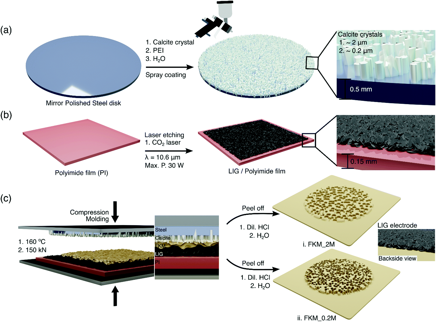 | ||
| Fig. 1 Fabrication of transfer-printed micropatterned FKM film and LIG electrode: (a) schematic depiction of the transfer-printable mold prepared by spray coating of colloidal calcite/polyethyleneimine (PEI) solution. (b) CO2 Laser irradiated fabrication of LIG on a PI substrate. (c) Direct imprinting of both the active surface and LIG electrode on a tribonegative precured FKM substrate. Prior to compression at 160 °C, the precured FKM was mixed with organic peroxide curing agent (2,5-dimethyl-2,5-di-(tert-butylperoxy)hexane (DHBP), 2 wt%) and coagent (Triallyl isocyanurate (TAIC), 3 wt%) and masticated for 10 min. | ||
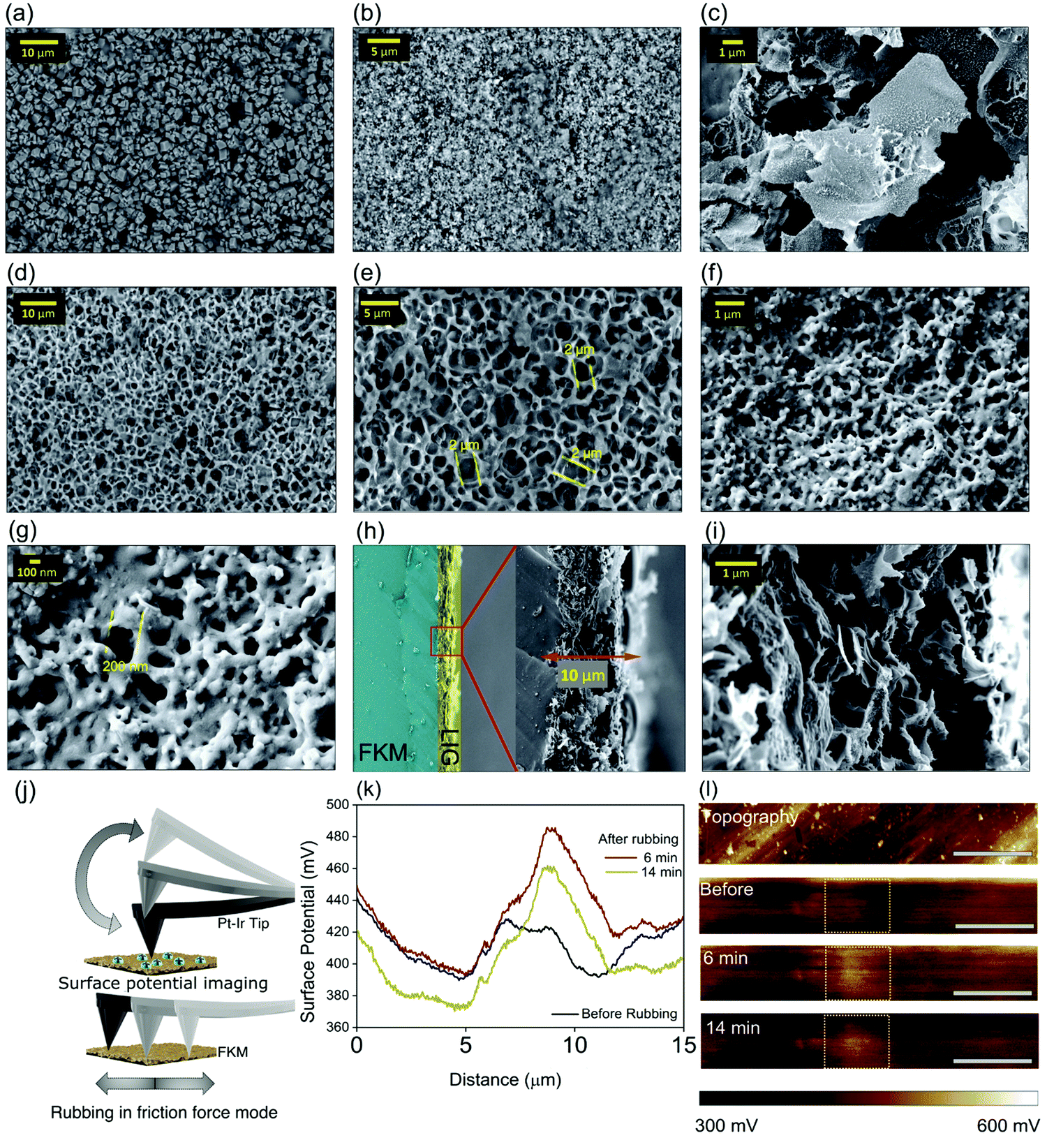 | ||
| Fig. 2 Surface morphological characterization of the active micropatterned FKM and LIG electrode. SEM images of transfer-printable molds: (a) printable disk for FKM_2 M, with uniformly spaced microcrystals (average size ∼2 μm) of calcite, (b) printable disk for FKM_0.2 M containing calcite nanocrystals (200 nm), (c) surface morphology of LIG/PI. Resulting surface morphological scanning electron micrograph of micropatterned (d and e) FKM_2 M, (e and f) FKM_0.2 M and (g and h) cross-sectional FESEM of transferred LIG electrode on FKM substrate. Transferred LIG electrode reveals characteristic graphene platelet morphology with average layer thickness of 10 μm. Mechanism of triboelectric effect elucidated by AFM-KPFM studies. (j) Schematic description of the KPFM process, (k) surface potential distribution of the relaxation process for FKM film, before and after ‘rubbing’, (l) time evolution map in terms of surface potential before and after contact electrification. Note the measured contrast difference between the rubbed (3 μm × 3 μm) and un-contacted region. Scale bar measures 4 μm. | ||
The surface micropatterns of FKM_2 M and FKM_0.2 M are shown in Fig. 2(d–g), respectively. High surface porosity coupled with homogeneity in pore distribution for both FKM substrates is considered crucial for friction-induced enhanced surface charge density and triboelectric outputs. Owing to the smaller dimension of calcite crystals (200 nm), porosity and surface area are shown to be higher in FKM_0.2 M. The EDAX elemental mapping of the micropatterned FKM_2 M and FKM_0.2 M surfaces shown to preserve high F-content and are illustrated in Fig. S6 and S7, (ESI†) respectively. Following the transfer under compression molding, the LIG films adhered well to the FKM substrates and sustained robust mechanical stretching and friction. The cross-sectional SEM images of LIG/FKM electrode are shown in Fig. 2(h and i). The thickness of the LIG film is 10 μm. The characteristic flaky graphene platelet-like morphology (Fig. 2i) ensures electrical contact even under mechanical twisting and stretching (200%). Additional Raman spectroscopic characterization of LIG on PI substrate can be found in ESI† (Fig. S8).
The intrinsic triboelectric characteristics and friction-induced accumulation/dispersion of electrostatic potential on FKM film (thickness 0.18 mm) are investigated by Kelvin probe force microscopy (KPFM). Initially, KPFM is conducted on the FKM film to determine the surface potential for an area of approx. (20 × 3) μm2. Following the process illustrated in Fig. 2j, triboelectric contact charges are deliberately created on the FKM surface using a load force of ∼10 nN. The corresponding friction force is 6 nN which was deduced from the lateral distortion difference of the AFM tip between the forward and reverse directions. Following the rubbing step, measurement is changed to KPFM mode immediately. The surface potential distribution for the FKM film at different time intervals is plotted in Fig. 2k. Corresponding series of surface potential distribution images recorded at particular intervals are shown in Fig. 2l. Owing to the complex morphological, electrical, and surface properties, the mechanism of triboelectric effect for FKM/LIG STENG appears to be complex. However, a quantitative approximation of the charge transfer phenomenon between the electrode and dielectric film can be directly correlated to the effective work functions of the corresponding components.23 As the FKM elastomer is composed of vinylidene fluoride (VDF), the work function appears to be ∼5 eV, whereas for the Pt-Ir coated cantilever tip, the work function is estimated to be 5.5 eV.24 Therefore, charge flows from the FKM surface to the tip, resulting in a net positive electrostatic charge distribution as shown in Fig. 2(k and l).18 For the graphene electrode, however, the effective work function varies between 4.3–4.7 eV.25 As the work function of FKM can hardly be influenced by the tip friction force, the lighter contrast in the scanned area on FKM implies the transfer of tribo-charge following the ‘rubbing’ by cantilever tip, resulting in accumulation of net positive potential. The histogram analysis of the surface potential shows a mean potential of 410 mV and a maximum of 471 mV for 3 μm x 3 μm friction area. After rubbing stage, corresponding potential distribution changed to 468 mV (min.) and 531 mV (max.) after 6 min, and to 436 mV (min.) and 508 mV (max.) after 14 min, respectively. Therefore, it is observed that accumulated positive potential (Fig. 2l) persisted for over 14 min and beyond, signifying a slow relaxation and superior triboelectric performance. The downward trends for the baseline post-14 min could be associated with the tip effect: when the tip picks up a particle or is otherwise contaminated, the measured surface potential would change due to the shielding of charges. In our case, the curves have the same shape for both the FKM substrates, so we suspect that it could have shifted the post-14 min curve to nearly 25 mV up.
To illustrate the triboelectric output of the LIG/micropatterned FKM films, a single electrode TENG (STENG) is constructed and mounted on the Cu-plates of an in-house developed vertical contact-separation device controlled by a pneumatic actuator. The detailed illustration of the custom triboelectric set up is demonstrated in ESI.† The maximum force applied during contact mode between the tribolayers is 15 N cm−2. As stated before, FKM is considered to be tribo-negative layer with respect to LIG electrode. The output open circuit voltages (VOC) are generated for the three STENGs: FKM (Fig. 3a) FKM_2 M (Fig. 3b) and FKM_0.2 M (Fig. 3c) as functions of frequency of operation (1–5 Hz) and thickness of tribo-negative FKM layer. During the vertical contact-separation mode, coupled effect of triboelectrification and subsequent electrostatic induction brings about large output VOC in the external circuit. The FKM layer acts as an active tribonegative layer whereas the LIG is connected to the ground as a reference electrode. The gap between the top and bottom layers kept consistent at 2 cm. The measured output for the open-circuit voltage (VOC) predictably increase with the extent of surface micro-porosity. With the mean diameter of the porous well on FKM (∼2 μm to 200 nm) increasing, effective contact surface between the layers also shown to increase.19,26 As surface charge density is directly proportional to triboelectric outputs, FKM_0.2 M with highest surface roughness eventually results in maximal VOC (148 V, VPP ≈ 234 V) followed by FKM_2 M (136 V, VPP ≈ 215 V). As stated earlier, working principle of STENG for harvesting mechanical energy relies on the coupled effect of triboelectric contact charging and separation-inflicted electrostatic induction.3–5,7,27 In brief, FKM microporous film works as an active layer whereas the LIG electrode is connected to ground as reference. Following the contact, triboelectrification results in net accumulation of negative changes on FKM surface. At this point, tribo-charges with opposing polarities produced are balanced and no current flows in the external circuit. During separation, a potential drop is emerged that propels the electrons to respective electrodes and consequently, output current signal is generated.5,15 Eventually the flow of electrons stops when the distance between the FKM and LIG electrode reached a critical point (equilibrium state). Afterwards, as soon as the layers approach other, induced charges on LIG electrode transmitted to ground to equilibrate until the contact mode kicks in. When the contact established again, the STENG system comes back to the primary state.28 Therefore, a full cycle triboelectric output generation process for the microstructured FKM STENG is completed. Fig. 3d presents the open circuit voltage (VOC) output of STENGs derived from transfer-printed microstructured FKM/LIG films at 5 Hz. The typical thicknesses of the FKM films are 0.18 mm. The output voltage generated in one oscillation cycle is shown in Fig. 3e. Apparently, the FKM_0.2 M based-STENG performs well over the operating frequency range of 1–5 Hz as continuous periodic output voltage waveform is generated over the operating range (Fig. 3f). As flow of electrons in the external circuit reaches the equilibrium state faster with higher frequency, nearly 200% increase in VOC is reported when the frequency is varied from 1 Hz to 5 Hz. At higher frequencies, incomplete charge neutralization triggers the accumulation of charges on the electrode, resulting in overall higher VOC output.29 The voltage waveforms for all the specimens are shown to be asymmetric. Since the electrode separation gap is much larger than the FKM film thickness, contact-to-separation motion gives rise to higher VOC (top part), while the separation-to-contact motion leads to lower VOC.30 Increasing the FKM layer thickness could have resulted in greater symmetry; however, higher thickness resulted in lower output voltage in our case and are discussed in the proceeding section. In addition, charge density and charge quantity (of dielectric FKM) could also impact the overall output voltage and asymmetric voltage profiles in the STENG modules.30
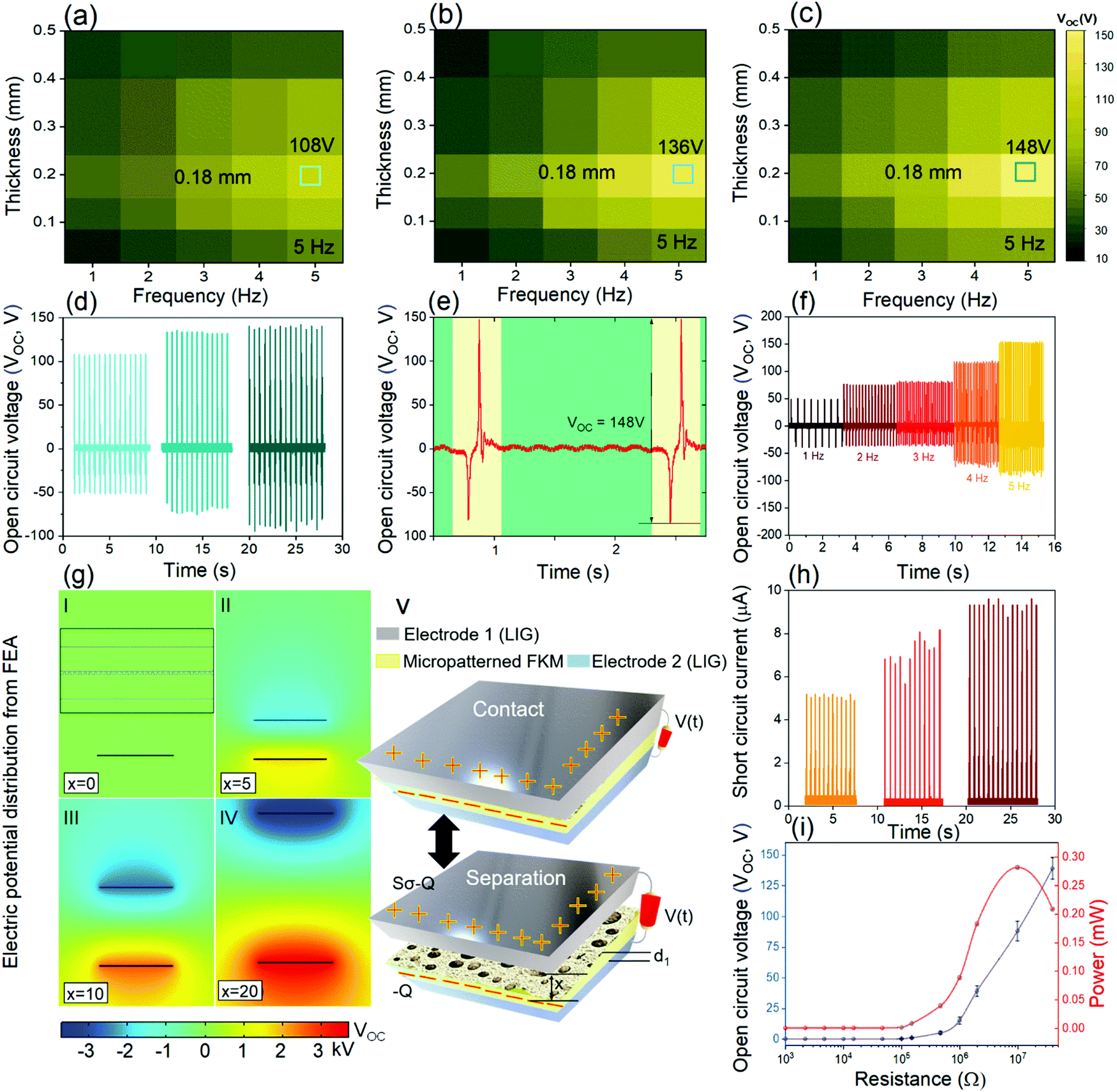 | ||
| Fig. 3 Output performance and working mechanism of FKM/LIG STENG. (a–c) Effect of thickness of FKM tribolayer and frequency of vertical contact-separation mode on the triboelectric open circuit output voltage (VOC) for FKM, FKM_2 M and FKM_0.2 M, respectively. (d) Maximum output VOC for FKM, FKM_2 M and FKM_0.2 M at 5 Hz and 15 N cm−2. FKM_0.2 M with highest surface porosity exhibits highest VOC (148 V) followed by FKM_2 M (136 V). (e) Output VOC in one oscillation cycle for FKM_0.2 M with peak-to-peak (VPP) voltage is estimated to 234 V. (f) Effect of operating frequency (Hz) on the output voltage. VOC is directly proportional to operating frequency range (1–5 Hz). (g, I–IV) Finite element simulation of electrostatic potential distribution with respect to separation distance (d) between FKM and LIG electrode, inset shows a zoomed-in section of tribo-surface geometry constructed for the finite element calculation, (V) a schematic of triboelectric charge transfer mechanism in FKM/LIG-based conductor-to-dielectric STENG, (h) rectified short circuit current waveforms for the three STENGs containing FKM/LIG, FKM_2 M/LIG and FKM_0.2 M/LIG, (i) output voltage and power of the FKM_0.2 M/LIG STENG under different load resistance. | ||
Influence of surface patterning on the output electrical potential distribution of STENG was analyzed using COMSOL Multiphysics® software package as shown in Fig. 3g. The constructed model for finite element analyses is based on actual device dimension of 10 mm × 10 mm with the thickness of the FEM_0.2 M layer (d0) and LIG electrode are 0.18 mm and 10 μm, respectively. The periodic surface patterns are created in terms of 2D square well with depth and periodicity kept at 2 μm. The thickness of top LIG electrode is also maintained at 10 μm.
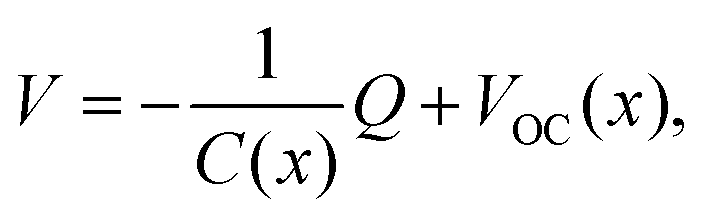
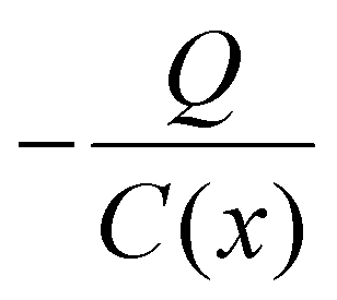
To ascertain the theoretical basis of a conductor-to-dielectric STENG under planar configuration, parallel-plate capacitor model has been employed widely and is based on two key assumptions: amount of charge Q is evenly distributed on the surface of the dielectric FKM surface and only perpendicular electric field component to the plate inside dielectric has to be considered while the parallel component is neglected. Following contact-separation, FKM substrate and primary LIG electrode acquire a net charge density of −σ and +σ, respectively. If transfer charges from dielectric-to-conductor is referred to as Q, total amount of charge at primary and reference electrode would be (σ–Q) and Q, respectively.31 Based on the model, Niu et al. derived the V–Q–x relationship for the contact mode TENG correlating the three important parameters: output voltage (V) and transfer charge (Q) with the electrode separation distance x as:
 | (1) |
 are potential differences from polarized charges and transfer charges, respectively.32 Considering length and width of the tribolayer being higher than the thickness (d1), and area (S) of the electrodes much greater than x, VOC(x) and C(x) can be expressed as,
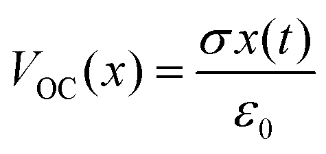 | (2) |
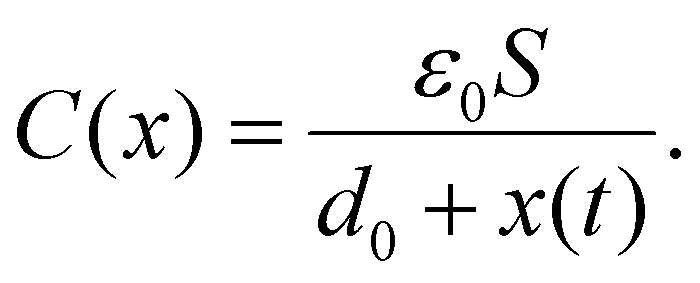 | (3) |
Substituting these values, the final V–Q–x expression for conductor-to-dielectric STENG is derived as follows:
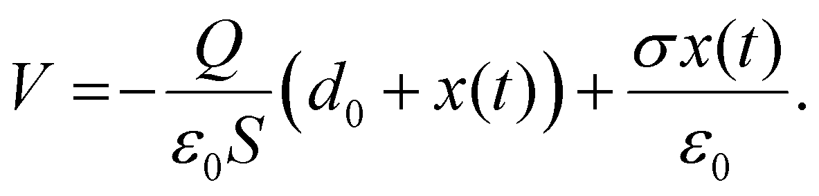 | (4) |
In the expression, d0 is the ratio of the thickness (d1) and relative permittivity of the FKM tribolayer, respectively. The above expression for contact-mode TENG can further be simplified under both open circuit and short circuit conditions as open circuit voltage, 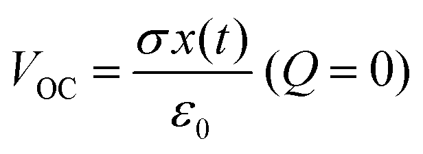 and short circuit current
 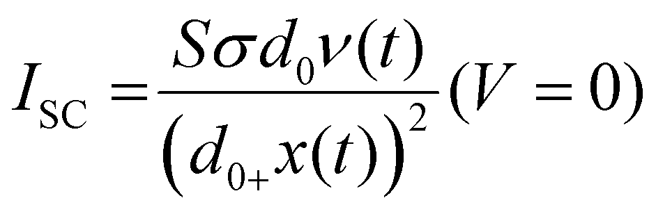 , respectively. It is evident from both the equations that, VOC and ISC are directly proportional to the triboelectric surface charge density (σ) which is a function of intrinsic material property and surface roughness of the triboelectric active substrates. Moreover, is shown to be directly proportional to the electrode separation gap (x) and it corroborates well to the simulation results in this case. The separation distance (x) between dielectric-to-conductor STENG (dielectric constant of FKM used in calculation is in the range 3–4) is varied from 0 to 20 mm and corresponding electrical potential distribution is shown in Fig. 3g(I–IV). With increasing x, potential distribution in terms of VOC also increases. A schematic of the triboelectric charge transfer mechanism for conductor-to-dielectric configuration based STENG configuration is presented in Fig. 3g(V). The rectified short circuit current (ISC) for the three STENGs has been evaluated to be 5, 6.5 and 9.6 μA, respectively. Corresponding waveforms are shown in Fig. 3h. To calculate the output power of the STENG derived from FKM_0.2 M, series of resistances are connected to the external circuit and corresponding voltage, current and power are evaluated (Fig. 3i). Predictably, output voltage decreases with increased load resistance whereas, output power reaches to a maximum of 0.28 mW at an external resistance of 10 MΩ. The corresponding power density is measured to be impressive 715 mW m−2. The output transfer charge and charge density of the FKM_0.2 M-based STENG are calculated to be 76 nC and 190 μC m−2, respectively. Along with excellent stretchability, FKMs are regarded as highly robust rubbers with exceptional thermal (thermal degradation starts at 488 °C, Fig. S9, ESI†) and chemical stability.33 These remarkable traits often considered to be quintessential feature for resilient applications in engineering and high-end electronic devices alike. The detailed mechanical characterizations are discussed in ESI† (Fig. S10). The elongation at break for FKM substrates is reported to be ∼290% (Table S2, ESI†). In terms of output power density of stretchable TENGs reported in recently published literature, FKM_0.2 M based STENG fared exceptionally well (for comparison with respect to recently reported stretchable TENGs, see Table S3, ESI†). Effect of FKM_0.2 M thickness plays an important role and we observed that a critical optimum thickness for the construction of STENG is 0.18 mm, below or beyond which, the triboelectric output becomes dissatisfactory (Fig. S11a, ESI†). A thinner dielectric layer is more efficient in transferring the accumulated charges on surface. However, below a critical thickness, separation of charges appeared to be hindered. Therefore, we kept the effective thickness of FKM_0.2 M at 0.18 mm. Additionally, we demonstrated triboelectric VOC output for STENG under various strain%, ranging from 0–200% (Fig. S11b and c, ESI†). A decrease in overall output over the strain range is obvious and can be interpreted in terms of apparent decrease of STENG thickness (Fig. S11c, ESI†).29
In order to ensure long term stability and output performance, a durability test was conducted for 3000 cycles under constant frequency of 5 Hz. As observed from Fig. 4a, the output VOC for FKM_0.2 M/LIG-based STENG are effectively unaltered even after 3000 cycles, providing a consistent output performance throughout. For the commercialization of STENG-based tactile sensors, long term operational stability is considered pivotal to its performance score.34 Provided the micropatterned FKM is derived from highly resilient rubber compound with higher abrasion resistance than most known substrates, STENG reported are highly robust and suitable for long term deployment in self-powered devices. To validate the effectiveness and superiority of the LIG-electrode, several other metallic and non-metallic electrodes were employed with the STENG. The output VOC for STENG/E (E = Cu tape, Carbon tape, Al adhesive film, Ag paste) sensors were recorded under identical conditions (5 Hz, 23 °C, 15 N cm−2 contact force) and compared to that of the output from FKM_0.2 M/LIG STENG (Fig. 4b). Evidently, for the LIG-based STENG, VOC appeared to be significantly higher than that of other metallic electrodes and to a good extent, the carbon tape. The later offers nearly comparable output, however, due to limit in stretchability in contrast to active FKM layer, the scope of application of a carbon tape-STENG appeared considerably restricted. We have conducted the sheet resistance of the LIG/FKM film under stretching condition and observed that the sheet resistance of the LIG film (130 Ω sq.−1) only increases slightly (180 Ω sq.−1) when the specimen was stretched (up to 100%). This could be most likely attributed to the LIG micro-texture, originated during the laser irradiation of the PI film (Fig. 2h). Conducting pathways were remained intact during the stretching cycles along the direction of the laser etching line. It is, therefore, apparent that conducting pathways persisted even under higher elongation so as to produce the electrical contact during contact-separation process in a typical triboelectric set up.
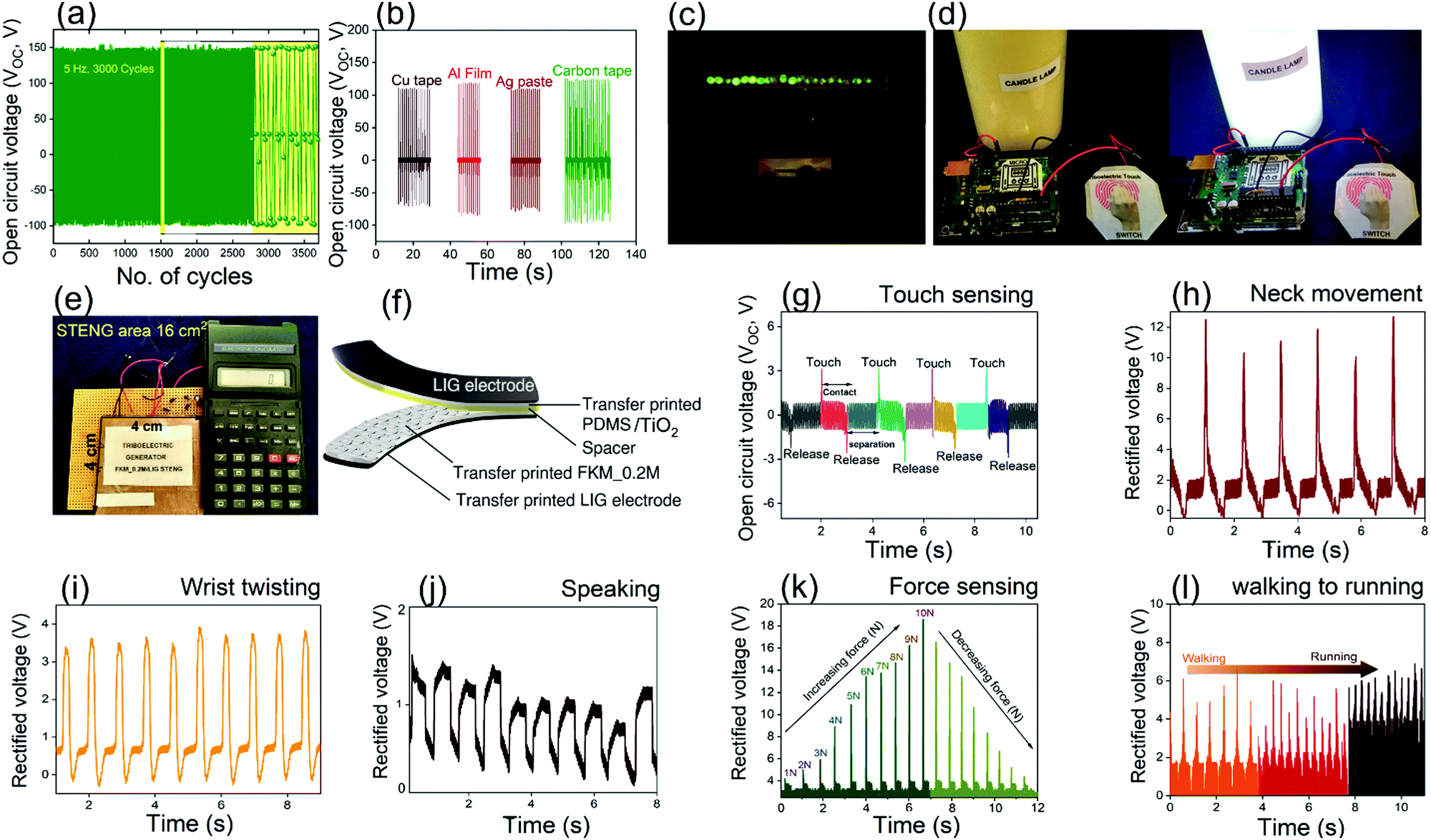 | ||
| Fig. 4 Performance of the stretchable metal-free FKM_0.2 M/LIG STENG. (a) Durability test of the STENG at 5 Hz for over 3000 cycles. (b) Effectiveness of metal-free LIG electrode over various metal and non-metallic electrodes (Cu tape, Carbon tape, Al adhesive film, Ag paste) is shown in terms of VOC (5 Hz). (c) Instantaneous output power generation from ambient mechanical motion is demonstrated in terms of illumination of 20 LEDs connected in series to DC-based STENG (16 cm2). (d) FKM_0.2 M/LIG-based electronic skin can be used as smart switch to turn on/off a lamp. (e) Image of an electronic calculator running by a capacitor (10 μF) directly charged with DC-based STENG harvester. (f) Schematic illustration of a dielectric-to-dielectric TENG incorporating FKM_0.2 M and micropatterned PDMS/TiO2 layer. (g) Real time rectified voltage vs. time signals for the TENG-based touch sensor illustrating on (touch) and off (release) switching response. (h) Voltage waveform signal for human neck movement in horizontal direction. (i) Rectified voltage signal with respect to time for wrist twisting motion. The sharp, distinguished signal could be beneficial for potential health monitoring applications. (j) The TENG sensor could detect vocal cord vibration while speaking. The signal detects mild response in terms of voltage waveform while speaking. (k) The TENG sensor module can also be employed as force sensor. (l) A knee-mounted TENG sensor could differentiate walking and running and depending on the periodicity of the motion, signals vary. | ||
To demonstrate that the FKM_0.2 M/LIG STENG can be effectively harvest mechanical motion and produce output power, we devised a simple set up connecting the larger contact area STENG (16 cm2) to 20 green LEDs simultaneously in series. From the eqn (4), it's evident that contact area of the electrode directly affects the overall voltage output. For instance, for the FKM_0.2 M based STENG (area ≈ 3.5 cm2), the output voltage (VOC) was observed to be 148 V, whereas, under similar conditions (contact force 15 N cm−2 and frequency 5 Hz), output voltage would increase to a value of ∼200 V for the contact area of 6 cm2).
The illumination of the LEDs during mechanical contact-separation mode is shown in Fig. 4c (for the video, please refer to ESI† Movie S1). For the STENG, a maximum power output of 0.8 mW is reported at a load resistance of 10 MΩ. Furthermore, the STENG-based electronic skin can be exploited to design intelligent switch for smart home solutions that can interpret command and perform operations. Fig. 4d illustrates a setup containing a microcontroller, STENG switch and a light source that can be extinguished and turned on using the smart touch switch. For video, please refer to ESI† Movie S2. The details of the circuit and setup are shown in ESI† (Fig. S12). To exhibit the self-power performance of the STENG, a commercial 10 μF capacitor is charged up to 3 V by taping the fingers approximately with 2 Hz frequency. The charged capacitor can be employed to run an electronic calculator, as shown in Fig. 4e (Movie S3, ESI†). This substantiates the fact that the STENG output could actually be sufficient to power low intensity electronics and sensing devices.35
Owing to the high triboelectric output of the FKM_0.2 M-based STENG in vertical contact-separation operation, a potential application could further be extended to construct a dielectric-to-dielectric TENG for tactile and force sensing. Surface engineered PDMS membranes have already been used for triboelectric tactile sensing and human motion detection applications.34,36,37 Following the similar protocol employed for FKM, we have incorporated transfer-printed PDMS/TiO2 film as positive tribolayer, whereas, FKM_0.2 M was taken as the active tribo-negative layer. The average pore size of the PDMS micropattern surface was identical to that of FKM_0.2 M (200 nm). High K-TiO2 nanometric (100 nm) layer was deposited by electron beam induced evaporation. The LIG electrode from LIG/PI was transferred onto the rear side of PDMS/TiO2 layer by simultaneously curing the PDMS in between the micropatterned mold and LIG/PI at 80 °C. For details on fabrication, please refer to ESI† (Fig. S13). A prototype of the dielectric-to-dielectric TENG-based tactile sensor is illustrated schematically in Fig. 4f. The resulting sensor is shown to detect subtle human motions and physiological signals, including touch, neck rolling, wrist twisting, speaking, detecting the force and running (Fig. 4g–l). Depending on the amplitude of the movement, output rectified voltage signal could vary between 1 V to 19 V. The characteristic waveforms are movement exclusive, i.e., voltage signal for speaking is distinctively different from that of wrist twisting or neck rolling. The tactile sensor based on micropatterned FKM/PDMS/LIG, therefore, is capable of detecting and distinguishing wide ranges of human touch/motion and highly desirable in terms of potential application in patient monitoring systems and artificial E-skin.
Conclusions
In summary, we incorporated transfer-printable, high F-content FKM for the construction of metal-free STENG comprising LIG electrode. The FKM substrate was cured in presence of organic peroxide and a coagent during the transfer printing process under compression at 160 °C. The printable molds were prepared by spray coating of colloidal solutions of surface modified calcite micro/nanocrystals of chosen dimensions onto mirror-polished steel disk. The resulting porous microwell-based FKM surface exhibited superior triboelectric power density of 715 mW m−2 at a matching resistance of 10 MΩ. The ultrastretchable STENG can generate maximum open circuit voltage and current of 148 V and 9.6 μA, respectively at the frequency of 5 Hz and maximum contact force of 15 N cm−2. For the first time, our work reported direct imprinting of both the active surface and LIG electrode on a tribonegative fluorinated rubber that appeared to offer an array of exciting outcomes in terms of the FKM's outstanding chemical and thermal stability, stretchability and superior imprinting efficiency. In order to illustrate the applicability of STENG in ambient mechanical energy harvesting, several demonstrations were also presented. Finally, owing to the STENG's excellent touch sensitivity, a tactile sensor based on dielectric-to-dielectric TENG using FKM (negative tribolayer) and micropatterned PDMS/TiO2 was constructed. The resulting TENG-based sensor has remarkable touch and motion sensitivities. In addition, the TENG could also detect mild human touches and interpret various physiological movements with high sensitivity and therefore, can be embedded onto soft robotic actuators for potential e-skin/bionic skin applications in health and human-machine interfaces.Experimental section
Fabrication of the transfer printing mold
Mirror-polished stainless-steel disks with a diameter of 50 mm and a thickness of 0.5 mm served as substrates. Precipitated calcium carbonate (PCC, Schaefer Kalk GmbH & Co KG, Germany) and highly branched polyethylene imine (PEI, Mw = 750 kg mol−1, Sigma-Aldrich) were used for mold preparation. Rhombic PCC particles with two different sizes (2 μm and 200 nm) were used. A dispersion of PCC was prepared by mixing the appropriate amount of PCC and PEI with water and stirring for 12 hours. The typical concentration was 1% by mass for PCC and 0.1% by mass for PEI. Layers of PCC and PEI were prepared on the substrates by spraying a PCC dispersion for 30 s with an airbrush gun.LIG/PI synthesis by laser irradiation
In order to produce LIG on the PI (DuPont Kapton® film, 0.15 mm) surface, a degradation process of the polymer was introduced thermally by absorption of laser photons. A commercial CO2 laser system (Laser Tools and Technics Corp., Taiwan) was used with a wavelength of 10.6 μm, maximum output power of 30 W, and a maximum scan rate of 1524 mm s−1. The cleaned PI film was placed on a honeycomb stage and N2 gas was purged onto the surface during the laser irradiation. CorelDRAW Graphics® software was employed to control the laser parameters such as power, scan rate, and pulse density. The total energy of the laser over the area for the optimum process was calculated to be 19.4 J cm−2 with 50% of laser power, 100% of scan speed, and 500 pulses per inch in focus mode.Fabrication of transfer printed STENGs with LIG electrode
Prior to imprinting under compression, the fluoroelastomer (FKM, Tecnoflon P549L, Solvay) was mixed with peroxide curing agent DHBP (Sigma-Aldrich, 2,5-dimethyl-2,5-di-(tert-butylperoxy)hexane (DHBP), 2 wt%) and coagent (Sigma-Aldrich, triallyl isocyanurate (TAIC), 3 wt%). The mixing was done at 60 °C in a two-roll mill mixer (Polymix 110L, Servitech GmbH, Germany) with friction ratio of 1![[thin space (1/6-em)]](https://www.rsc.org/images/entities/char_2009.gif) :1.2. Total duration of mixing was 10 min. Following the compounding, the masticated, precured film was placed in a compression molding apparatus (Fontijne Holland, TP400), placing the printing mold on top and LIG/PI substrate at bottom. The curing time (calculated from rheometric studies) and temperature was 6 min and 160 °C, respectively. Afterwards, the cured specimen was removed and detached simultaneously from printing steel disk and PI film on top and bottom, respectively. While the LIG has been successfully transferred to the FKM substrate, the micropattern created on top layer by impression was subjected to mild acid (HCl, 0.1 M) treatment to dissolve remaining calcite crystals stuck on the pores. Finally, the LIG/FKM film was stored in a desiccator. For the fabrication of micropatterned PDMS/LIG, similar printing disk and LIG/PI were employed on which the precured PDMS (Sylgard® 184, with 1:8 monomer to crosslinker ratio) was casted upon and left for curing at 60 °C for 4 h. The final thickness of the PDMS layer was maintained at 0.10 mm.
:1.2. Total duration of mixing was 10 min. Following the compounding, the masticated, precured film was placed in a compression molding apparatus (Fontijne Holland, TP400), placing the printing mold on top and LIG/PI substrate at bottom. The curing time (calculated from rheometric studies) and temperature was 6 min and 160 °C, respectively. Afterwards, the cured specimen was removed and detached simultaneously from printing steel disk and PI film on top and bottom, respectively. While the LIG has been successfully transferred to the FKM substrate, the micropattern created on top layer by impression was subjected to mild acid (HCl, 0.1 M) treatment to dissolve remaining calcite crystals stuck on the pores. Finally, the LIG/FKM film was stored in a desiccator. For the fabrication of micropatterned PDMS/LIG, similar printing disk and LIG/PI were employed on which the precured PDMS (Sylgard® 184, with 1:8 monomer to crosslinker ratio) was casted upon and left for curing at 60 °C for 4 h. The final thickness of the PDMS layer was maintained at 0.10 mm.
Characterization
The rheometric studies were performed in a moving die rheometer (Scarabaeus SIS-V50, Germany) at 160 °C and optimum curing time (t90) was calculated from time-torque plot. The dynamic mechanical properties of the FKM were investigated using Eplexor 2000N (Netzsch Gabo Instruments GmbH). Rectangle specimens of 35 × 10 × 2 mm3 dimension was cut out from the sheet. The temperature range was set from −80 to 150 °C at a heating rate of 2 K min−1. The frequency of the test was 10 Hz under 0.5% dynamic strain and 1% static strain. Tensile measurements are performed using Zwick 1456 tensile tester (ZwickRoell GmbH, Germany) equipped with optical strain measurement. A crosshead speed of 200 mm min−1 is used. Scanning electron micrographs of sample morphologies were captured using a Neon 40 FIB-SEM workstation (Carl Zeiss Microscopy GmbH, Germany). Scanning electron micrographs of transfer-printable molds were carried out using a Phenom XL Workstation from Thermo Scientific (Waltham, USA). The samples were sputter coated (Leica) with 3.5 nm of Platinum (Pt) prior to SEM. The measurement of the surface potential was performed in the KPFM (AM) mode by a Dimension ICON (Bruker-Nano, USA) using a conducting SCM-PIT V2 cantilever (Bruker-Nano, USA). The initial scan of topography and surface potential made on a 20 μm × 3 μm area. Thereafter the sample was scanned in the friction force mode by the same cantilever, electrically grounded, on a 3 μm × 3 μm area for 3 minutes. Immediately after, AFM mode switched back to KPFM mode to measure twice the surface potential with different time intervals, i.e., 6 min and 14 min. The current/voltage characterization of STENG and TENG were performed in an in-house developed vertical contact-separation unit, connected to a Pneumatic actuator (Festo Corp.). The instrumentation details can be found in ESI† (Fig. S14). Total vertical contact force generated by the pneumatic motor was 15 N cm−2. For the current and voltage values, the STENG/TENG units were connected to a Rigol DS4024 Digital storage Oscilloscope and a Keithley electrometer (Keithley 6514), respectively. For the demonstrations, STENG/TENG were connected to bridge rectifier and various ceramic load resistors. The green LEDs (1.8–3 V) were used for the STENG (surface area 16 cm2) output demonstration.Author contributions
I. A.: conceptualization, methodology, investigation, visualization, writing – original draft, writing – review & editing; P. Z.: resources, methodology, investigation, validation; S. H.: investigation, visualization, writing – original draft; H. P.: resources, investigation, validation; A. K. G.: visualization, formal analysis; A. J.: investigation, methodology; S. C.: writing – review & editing; J. N.: conceptualization, methodology, writing – review & editing; G. H.: writing – review & editing, supervision, funding acquisition; S. W.: resources, project administration, writing – review & editing, funding acquisition; A. D.: resources, methodology, formal analysis, supervision, project administration, writing – review & editing, funding acquisition.Conflicts of interest
The authors declare no conflict of interest.Acknowledgements
This work is financially supported by Deutsche Forschungsgemeinschaft (DFG, German Research Foundation) project ID 330167 under SPP2100 program. I. A. thankfully acknowledges René Jurk and Holger Scheibner for mechanical experiments. G. H. & S. W. acknowledge the DFG (German Research Foundation) Project 380321452/GRK2430 for financial support.References
- S. Yao, P. Swetha and Y. Zhu, Adv. Healthcare Mater., 2018, 7 Search PubMed.
- J. C. Yang, J. Mun, S. Y. Kwon, S. Park, Z. Bao and S. Park, Adv. Mater., 2019, 31, 1904765 CrossRef CAS PubMed.
- D. Son, J. Kang, O. Vardoulis, Y. Kim, N. Matsuhisa, J. Y. Oh, J. W. To, J. Mun, T. Katsumata, Y. Liu, A. F. McGuire, M. Krason, F. Molina-Lopez, J. Ham, U. Kraft, Y. Lee, Y. Yun, J. B. H. Tok and Z. Bao, Nat. Nanotechnol., 2018, 13, 1057–1065 CrossRef CAS PubMed.
- W. Liu, M. S. Song, B. Kong and Y. Cui, Adv. Mater., 2017, 29 Search PubMed.
- J. Ma, J. Zhu, P. Ma, Y. Jie, Z. L. Wang and X. Cao, ACS Energy Lett., 2020, 5, 3005–3011 CrossRef CAS.
- S. Maiti, S. K. Karan, J. K. Kim and B. B. Khatua, Adv. Energy Mater., 2019, 9, 1803027 CrossRef.
- D. Larcher and J. M. Tarascon, Nat. Chem., 2015, 7, 19–29 CrossRef CAS PubMed.
- M. Sahu, S. Hajra, H.-G. Kim, H.-G. Rubahn, Y. Kumar Mishra and H. J. Kim, Nano Energy, 2021, 88, 106255 CrossRef CAS.
- S. K. Karan, S. Maiti, J. H. Lee, Y. K. Mishra, B. B. Khatua and J. K. Kim, Adv. Funct. Mater., 2020, 30, 2004446 CrossRef CAS.
- F. R. Fan, Z. Q. Tian and Z. Lin Wang, Nano Energy, 2012, 1, 328–334 CrossRef CAS.
- R. Hinchet, H. J. Yoon, H. Ryu, M. K. Kim, E. K. Choi, D. S. Kim and S. W. Kim, Science, 2019, 365, 491–494 CrossRef CAS PubMed.
- C. Wu, A. C. Wang, W. Ding, H. Guo and Z. L. Wang, Adv. Energy Mater., 2019, 9, 1802906 CrossRef.
- H. Zou, Y. Zhang, L. Guo, P. Wang, X. He, G. Dai, H. Zheng, C. Chen, A. C. Wang, C. Xu and Z. L. Wang, Nat. Commun., 2019, 10, 1427 CrossRef PubMed.
- L. Xu, L. Xu, J. Luo, Y. Yan, B. E. Jia, X. Yang, Y. Gao and Z. L. Wang, Adv. Energy Mater., 2020, 10, 2001669 CrossRef CAS.
- Z. L. Wang, Mater. Today, 2017, 20, 74–82 CrossRef.
- M. Choi, M. Humar, S. Kim and S. H. Yun, Adv. Mater., 2015, 27, 4081–4086 CrossRef CAS PubMed.
- J. Li, N. A. Shepelin, P. C. Sherrell and A. V. Ellis, Chem. Mater., 2021, 33, 4304–4327 CrossRef CAS.
- J. Ha, J. Chung, S. M. Kim, J. H. Kim, S. Shin, J. Y. Park, S. Lee and J. B. Kim, Nano Energy, 2017, 36, 126–133 CrossRef CAS.
- L. Lin, Y. Xie, S. Niu, S. Wang, P. K. Yang and Z. L. Wang, ACS Nano, 2015, 9, 922–930 CrossRef CAS PubMed.
- M. G. Stanford, J. T. Li, Y. Chyan, Z. Wang, W. Wang and J. M. Tour, ACS Nano, 2019, 13, 7166–7174 CrossRef CAS PubMed.
- H. Chu, H. Jang, Y. Lee, Y. Chae and J. H. Ahn, Nano Energy, 2016, 27, 298–305 CrossRef CAS.
- B. Sun, R. N. McCay, S. Goswami, Y. Xu, C. Zhang, Y. Ling, J. Lin and Z. Yan, Adv. Mater., 2018, 30, 1804327 CrossRef PubMed.
- H. H. Singh and N. Khare, Adv. Mater. Interfaces, 2021, 8, 2170068 CrossRef.
- R. Sydam, R. K. Kokal and M. Deepa, ChemPhysChem, 2015, 16, 1042–1051 CrossRef CAS PubMed.
- E. V. Rut’kov, E. Y. Afanas’eva and N. R. Gall, Diamond Relat. Mater., 2020, 101, 107576 CrossRef.
- F. R. Fan, L. Lin, G. Zhu, W. Wu, R. Zhang and Z. L. Wang, Nano Lett., 2012, 12, 3109–3114 CrossRef CAS PubMed.
- L. Cheng, Q. Xu, Y. Zheng, X. Jia and Y. Qin, Nat. Commun., 2018, 9, 1–8 CrossRef PubMed.
- S. Wang, L. Lin and Z. L. Wang, Nano Energy, 2015, 11, 436–462 CrossRef CAS.
- A. Das, T. S. Natarajan, S. Finger, J. Lacayo-Pineda, E. S. Bhagavatheswaran, S. S. Banerjee and G. Heinrich, ACS Appl. Electron. Mater., 2020, 2, 4054–4064 CrossRef.
- Z. Wang, W. Liu, J. Hu, W. He, H. Yang, C. Ling, Y. Xi, X. Wang, A. Liu and C. Hu, Nano Energy, 2020, 69, 104452 CrossRef CAS.
- S. Niu, Y. Liu, S. Wang, L. Lin, Y. S. Zhou, Y. Hu and Z. L. Wang, Adv. Funct. Mater., 2014, 24, 3332–3340 CrossRef CAS.
- S. Niu, S. Wang, L. Lin, Y. Liu, Y. S. Zhou, Y. Hu and Z. L. Wang, Energy Environ. Sci., 2013, 6, 3576–3583 RSC.
- J. Wei, S. Jacob and J. Qiu, Compos. Sci. Technol., 2014, 92, 126–133 CrossRef CAS.
- Y. W. Cai, X. N. Zhang, G. G. Wang, G. Z. Li, D. Q. Zhao, N. Sun, F. Li, H. Y. Zhang, J. C. Han and Y. Yang, Nano Energy, 2021, 81, 105663 CrossRef CAS.
- P. Cheng, H. Guo, Z. Wen, C. Zhang, X. Yin, X. Li, D. Liu, W. Song, X. Sun, J. Wang and Z. L. Wang, Nano Energy, 2019, 57, 432–439 CrossRef CAS.
- X. Xia, J. Chen, G. Liu, M. S. Javed, X. Wang and C. Hu, Carbon, 2017, 111, 569–576 CrossRef CAS.
- G. Z. Li, G. G. Wang, D. M. Ye, X. W. Zhang, Z. Q. Lin, H. L. Zhou, F. Li, B. L. Wang and J. C. Han, Adv. Electron. Mater., 2019, 5, 1800846 CrossRef.
Footnote |
| † Electronic supplementary information (ESI) available. See DOI: 10.1039/d2mh00074a |
| This journal is © The Royal Society of Chemistry 2022 |