
Inversion symmetry broken in 2H phase vanadium-doped molybdenum disulfide†
Hanjun
Jiang‡
a,
Lu
Zheng‡
abc,
Jing
Wang
d,
Manzhang
Xu
 abc,
Xuetao
Gan
*d,
Xuewen
Wang
*abc and
Wei
Huang
abcef
abc,
Xuetao
Gan
*d,
Xuewen
Wang
*abc and
Wei
Huang
abcef
aFrontiers Science Center for Flexible Electronics (FSCFE) & Shaanxi Institute of Flexible Electronics (SIFE), Northwestern Polytechnical University, 127 West Youyi Road, Xi'an, 710072, China
bShaanxi Key Laboratory of Flexible Electronics (KLoFE), Northwestern Polytechnical University, 127 West Youyi Road, Xi'an, 710072, China
cMIIT Key Laboratory of Flexible Electronics (KLoFE), Northwestern Polytechnical University, 127 West Youyi Road, Xi'an, 710072, China
dKey Laboratory of Light Field Manipulation and Information Acquisition, Ministry of Industry and Information Technology, and Shaanxi Key Laboratory of Optical Information Technology, School of Physical Science and Technology, Northwestern Polytechnical University, 127 West Youyi Road, Xi'an, 710072, China
eState Key Laboratory of Organic Electronics and Information Displays, Institute of Advanced Materials (IAM), Nanjing University of Posts & Telecommunications, 9 Wenyuan Road, Nanjing 210023, China
fKey Laboratory of Flexible Electronics (KLoFE) and Institute of Advanced Materials (IAM), Nanjing Tech University (Nanjing Tech), 30 South Puzhu Road, Nanjing 211800, China
First published on 27th September 2021
Abstract
Two-dimensional (2D) layered transition metal dichalcogenides (TMDs) have received much attention in nonlinear optical applications due to their unique crystal structures and second harmonic generation (SHG) efficiency. However, SHG signals in TMDs show a layer-dependent behavior, consistent with the presence (absence) of inversion symmetry in even-layer (odd-layer) of TMDs. Herein, we synthesized monolayer and bilayer 2H and 3R phase vanadium (V)-doped MoS2 crystal. Raman spectroscopy, XPS, and STEM were used to identify the chemical composition and crystalline structure of as-grown nanoflakes. SHG measurement was used to research the symmetry of V-doped MoS2 crystals with different stacking orders. Significantly, the SHG efficiency in bilayer 2H phase V-doped MoS2 is equivalent to the 3R phase, indicating an inversion symmetry broken lattice structure caused by the in situ V substitute for Mo sites. This study will be conducive to promote the development of promising nonlinear optical devices based on 2D material.
 Xuewen Wang | Xuewen Wang is a professor and deputy Dean of the Institute of Flexible Electronics at Northwestern Polytechnical University, China. He received his Ph.D. in materials science from Nanyang Technological University, Singapore. His research interests are in the area of flexible electronics and advanced functional materials for flexible healthcare sensors. He explored new materials such as 2D materials, and new micromanufacturing technology for highly-integrated flexible smart sensors. His group is devoted to developing in situ and ex situ characterization techniques to reveal the sensing and failure mechanism for flexible materials and flexible sensors at the nanoscale. |
Introduction
Two-dimensional (2D) transition metal dichalcogenides (TMDs), represented by MoS2, WS2, WSe2, MoTe2, have gained enhanced research interest in recent years. Many excellent physical properties were observed in atomically thin few layers or monolayer TMDs, such as high Young modulus,1–3 excellent transistor mobility and on–off ratio,4 as well as piezoelectricity,5,6 superconductivity7,8 and nonlinear Hall effect.9 These make the TMDs an ideal candidate for next-generation optoelectronic device.10,11 Typically, 2D TMDs possess three crystalline structure, trigonal prismatic 3R, 2H phase and octahedral 1 T phase, respectively.12,13 3R polytype has AA stacking order of adjacent layers in same crystalline orientation with a slight in-plane shift. Based on the AA stacking order, 3R phase crystals exist with parallel in-plane nonlinear dipoles due to the absence of inverse symmetry.14–16 Thus, 3R TMDs possess effective second-order nonlinear susceptibility (χ(2)) and phase-matched second harmonic generation (SHG) from monolayer to bulk crystal regardless of layer numbers. Distinguished from 3R polytype, 2H polytype TMDs have AB stacking order of adjacent layers in opposite crystalline orientation, leading to centrosymmetry (non-centrosymmetry) in even (odd) numbered layers.5,17,18 As a result, 2H TMDs present a layer-dependent SHG due to the broken or recovery of inverse symmetry, which limits the application of 2D TMDs in the nonlinear optical devices since most 2D TMDs acquired by CVD synthesis or mechanical exfoliation from bulk crystal is 2H phase.Currently, many strategies have been introduced to break the inverse symmetry of 2D TMDs and change the lattice structure,19–23 such as tunning by electric field or defects,24,25 strain regulation,9 twisted TMDs via artificial stacking,26,27 and controllable 3R phase crystal growth.14,15,28 Yu et al. measured a strong SHG signal in bilayer 2H WSe2 by applying an electrical gate field.24 Further bond-charge model analysis indicated that accumulated sub-monolayer screening charge in the tungsten plane resulting in a nonuniform field distribution. The nonlinear Hall effect was observed in monolayer WSe2 by applying uniaxial strain to break C3v symmetry.9 Apart from applying external condition, precise regulation of growth factor during 2D materials preparation process is a direct way to achieve crystalline phase control. Chen et al. fabricated the 3R-stacked MoS2 by homoepitaxial growth, and the flakes performed a vigorous SHG intensity by a factor of 6 compared with that of monolayer MoS2.15 Although 3R MoTe2, WS2 and WSe2 have been synthesized by CVD or PVD route and exhibited considerable SHG in even layers, the large-area and high-quality synthesis of a wide range of 2D TMDs remain big challenge up to now.13
Recently, atomic doping or alloy has been a common means in regulating electric and magnetic properties,7,29,30 and phase controlled-synthesis of 2D material.31,32 V-doped MoS2 with different concentrations has been reported in tunning the electric conductance from n-type to p-type.29 However, the nonlinear optical effect of 2D V-doped MoS2 has not been investigated systematically before. Polarization angle-dependent SHG of monolayer RexMo1−xS2 (0 < x < 0.16) demonstrated that a slight lattice strain emerged in 2H MoS2 due to Re substitute for Mo sites.33 It provides a promising possibility to change the symmetry of pristine 2D material by atomic doping.
In this work, we synthesized V-doped MoS2 flakes via CVD growth using MoO3 and V2O5 precursors. SHG measurement was employed to investigate the doping effect of bilayer flakes with different stacking orders for 2H phase AB stacking and 3R phase AA stacking. We find significant SHG efficiency in bilayer 2H phase V-doped MoS2 flakes compared with that of 3R phase, confirming a broken inverse symmetry regardless of crystalline orientation and layer numbers. We believe the significant result will promote the application of 2D materials in the nonlinear optoelectronic device. This work also provides a potentially valuable strategy for the design of 2D optical crystals with broken inversion symmetry.
Experimental section
CVD synthesis of V-doped MoS2
V-Doped MoS2 crystals were synthesized by chemical vapor deposition (CVD) under standard atmospheric pressure. Fig. 1a illustrates the synthesis process of V-doped MoS2 in this work. MoO3 (Aladdin, 99.999%), V2O5 (Aldrich, 99.99%) and S powder (Aladdin, 99.95%) were used as source materials for the synthesis of V-doped MoS2 crystal. A powder mixture of 2 mg NaCl, 4 mg MoO3 and 4 mg V2O5 in an aluminium oxide boat was placed in the center of the quartz tube. Especially, the source MoO3 and V2O5 powder were mixed uniformly in the mortar in advance. 100 mg S powder was placed at the upstream side of the furnace. The grown substrate SiO2/Si was placed on downstream of the aluminium oxide boat with ∼1 cm distance. The furnace was heated to the growing temperature 800 °C with a ramp rate of 35 °C min−−1 and the growth time was 5 minutes. After that, the furnace was decreased to room temperature naturally. Argon (Ar) with a flow rate of 80 sccm (standard cubic centimeters per minute) was used as the carrier gas.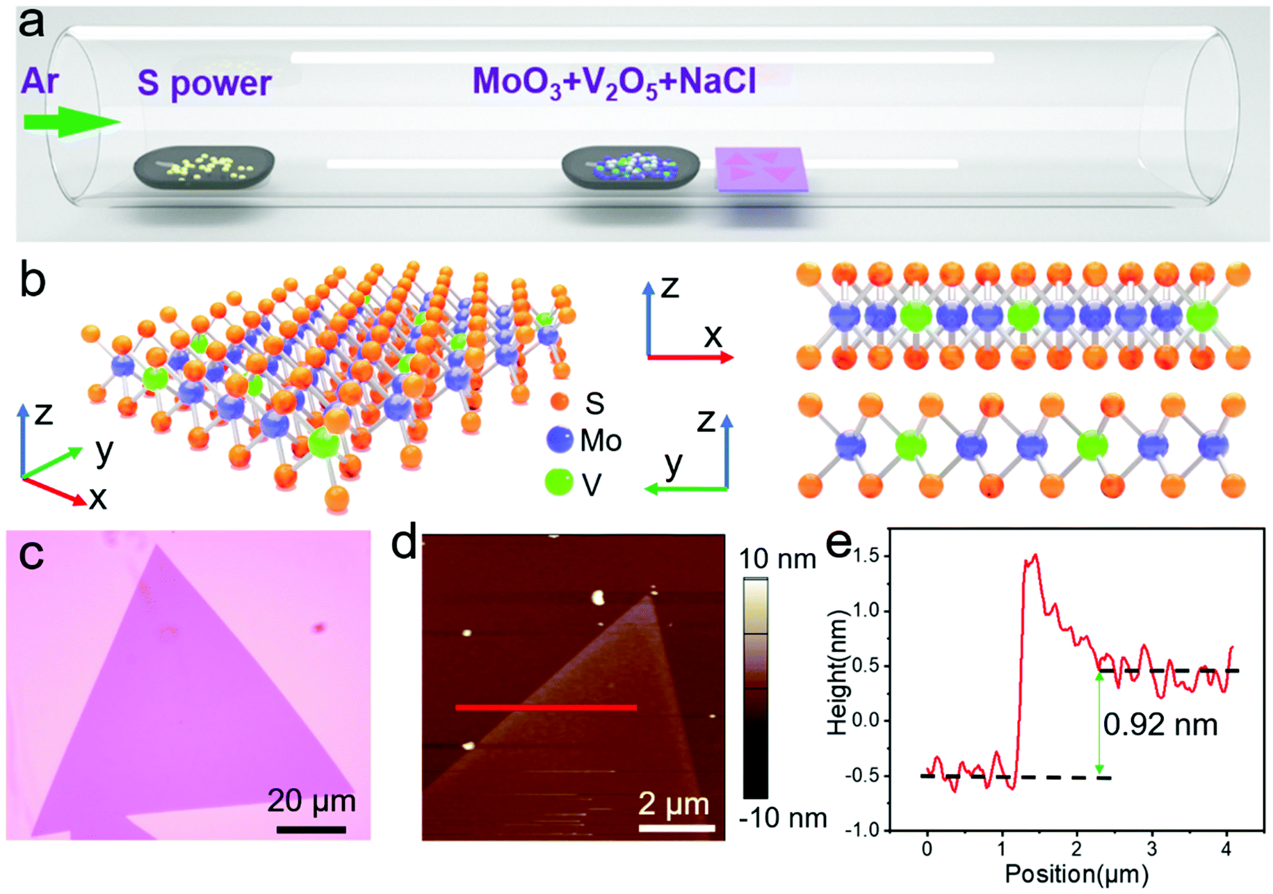 | ||
| Fig. 1 (a) Schematic of synthesis of V-doped MoS2 by CVD. (b) Atom structure and side view of V-doped MoS2. (c) Optical image of a V-doped MoS2 single crystal. (d and e) AFM topography and thickness measurement of V-doped MoS2. | ||
Characterization
Optical imaging was taken by ZEISS Primotech microscope. AFM topography and nanoindentation experiments were performed by Bruker Dimension Icon system. PL spectra and Raman mapping characterizations were carried out with the excitation laser of 532 nm using a WITEC alpha 300R Raman system. The system was first calibrated with the Raman peak of Si at 520 cm−1 before the Raman measurement of V-doped MoS2 flakes. The PMMA-assisted wet-transfer method was employed to prepare the HADDF-STEM sample. STEM imaging was performed by FEI Themis system at 200 kV.SHG measurement of the 2D V-doped MoS2 flakes was carried out in a home-built vertical microscope setup with the reflection geometry. A fiber-based pulsed laser with a central wavelength at 1550 nm, a repetition rate of 18.5 MHz, and a pulse width of 8.8 ps was used as the fundamental pump radiation, A microscope objective lens (50×) with a numerical aperture of 0.75 was employed to focus the pump laser into a spot size of about 2 μm on the sample. The second harmonic signal scattered from the sample was collected by the same objective lens. In the signal collection path, a dichroic mirror was used to filter out the pump laser from the SHG signal, which was finally analyzed and detected by a spectrometer mounted with a cooled silicon charge-coupled device camera.
Results and discussion
Monolayer or bilayer V-doped MoS2 flakes were synthesized by the salt-assisted CVD method, as shown in Fig. 1(a). Briefly, the mixed MoO3 powder, V2O5 powder and NaCl particles were placed in the center of the heating zone. The S powder was placed in the upstream. More detailed information can be found in the Experimental section. The atomic structure of monolayer V-doped MoS2 crystal was schematically shown in Fig. 1(b). The left panel in Fig. 1(b) gives its three-dimensional atomic structure, which is similar as the structure of 1H phase MoS2. The difference is that in the center layer of the sandwich, partial Mo atoms were replaced by V atoms. The side view from x–z direction and y–z direction in the right panel gives a clear sight. The optical image of the growing V-doped MoS2 flake was shown in Fig. 1(c). A single triangle crystal was observed with lateral size of about 90 μm. AFM measurement was used to characterize the topography and thickness of the flakes. Its corresponding result was shown in Fig. 1(d). The step height of 0.92 nm between the SiO2/Si substrate and the sample measured by line scan indicates a monolayer flake.Raman spectroscopy and X-ray photoelectron spectroscopy (XPS) characterization of the 2D V-doped MoS2 sheets were collected and presented in Fig. 2. Raman spectra of pristine monolayer MoS2 (black curve) and V-doped MoS2 (red curve) flakes were displayed in Fig. 2(a). Typical Raman characteristic peaks were observed from the pristine MoS2. The E2g1 mode at 384.5 cm−1 refers to the in-plane vibration of Mo and S atoms. The A1g mode at 403 cm−1 refers to the out-of-plane vibration of S atom. While with the doping of V atoms in MoS2 lattice, significant differences appear at the Raman spectra. Multiple peaks at 158 cm−1, 188 cm−1, 226 cm−1, 325 cm−1, 352 cm−1 were observed in the V-doped MoS2, which was coincident with the previous report.29,30 In particular, the peak at 226 cm−1 is the characteristic peak of disordered MoS2, which could be caused by the V atoms induced broken of lattice symmetry. In order to find out the distribution of V dopant, Raman intensity mapping of V-doped MoS2 flake was further carried out. As shown in Fig. 2(b), the upper left panel is an optical image of the sample, and the selected region is marked by a white frame. The homogeneous and uniform Raman intensity mapping of both E2g1 mode at 384 cm−1, A1g mode at 403 cm−1 and characteristic mode of disordered MoS2 at 226 cm−1 reveal the V atoms are uniformly doped throughout the entire nanoflakes. XPS measurement further demonstrates the existence of S, Mo, and V elements. Fig. 2(c–e) give the narrow spectrum of S 2p, Mo 3d, and V 2p state, respectively. The spectra of S 2p core level binding energy have two strong peaks at 161.3 eV and 162.5 eV, corresponding to S 2p3/2 and S 2p1/2. And the peaks of Mo 3d core level state at about 228.4 eV and 231.6 eV, corresponding to Mo 3d5/2 and Mo 2p3/2, respectively. The bonding states of S and Mo elements in the V-doped MoS2 alloy exhibit a slight energy shift compared with that of pristine MoS2 in the previous report.34,35 This can be explained by the effect of the nearby doped V atom. The red curve in Fig. 2(e) is the Gaussian fit of the signal of V 2p orbital split. Two strong peaks located at about 517.2 eV (2p3/2) and 524.0 eV (2p1/2), which is consistent with the original chemical state of V atom in a hexagonal structure, demonstrating the successful in situ replacement of Mo atom in MoS2 lattice.36 As shown in Fig. 2(e), the experimental result presented by black points is not so flat, indicating a low concentration doping of V atoms in the sample.
 | ||
| Fig. 2 Raman and XPS measurement of V-doped MoS2. (a)Raman spectra of pristine MoS2 and V-doped MoS2. (b) Optical image of V-doped MoS2 and its corresponding Raman intensity mapping images at 403 cm−1, 384 cm−1 and 226 cm−1. (c–e) XPS narrow spectra of the S 2p, Mo 3d, and V 2p orbitals, respectively. | ||
To assess the quality of the as-synthesized V-doped MoS2 flakes precisely, high-angle annular dark-field scanning transmission electron microscopy (HAADF-STEM), selected area electron diffraction (SAED) and energy dispersive X-ray spectroscopy (EDS) were employed to explore the crystalline structure and chemical composition of the sample. Fig. 3(a) is a low magnification STEM image of a monolayer V-doped MoS2 flake transferred on a copper screen. The edge of the nanofilm has been lapped over during the transfer process. The SAED pattern (Fig. 3(b)) taken from the flake exhibits regular hexagonally arranged diffraction spots, which can be fitted to the hexagonal lattice structure of MoS2. It means that no lattice mismatch generation with the doping of V atoms in MoS2. The high-resolution STEM imaging gives obvious evidence of in situ substitute between Mo and V atoms further. The aberration correction annular dark-field (ADF)-STEM imaging can provide the Z-contrast with atomic resolution, which is proportional to the quadratic square of the atomic number (Z). So, the Mo (Z = 42) site is bright and V (Z = 23) site is dark in the ADF-STEM imaging (Fig. 3(c)).
 | ||
| Fig. 3 HADDF-STEM characterization of monolayer V-doped MoS2. (a) Low magnification image of transferred V-doped MoS2 nanofilm on grid copper. (b) SAED pattern of H-phase V-doped MoS2. (c) HADDF-STEM image of V-doped MoS2. Partial V substitutes for Mo sites are marked by red arrow; (d and e) enlarged STEM image and its corresponding atomic distribution of Mo (blue), V (green) and S (yellow). (f) Z-Contrast intensity profile along the highlighted red dashed box in (d). (g) EDS spectra of V-doped MoS2 flakes, confirming the coexistence of Mo, V and S elements. | ||
As a contrast, STEM imaging of pristine MoS2 flakes was also characterized and no dark filed was found in the MoS2 lattice (Fig. S1†). Red arrows marked the substitute of Mo sites by V atoms. The calculated doping concentration of V is ∼8% by counting the number of Mo and V atoms in the image, which is the highest value of V-doping in MoS2 using V2O5 as the precursor. An enlarged HAADF-STEM image (Fig. 3(d)) and its corresponding atomic structure (Fig. 3(e)) show a detailed atom distribution. The intensity line profile marked by the highlighted red frame in Fig. 3(d) is shown in Fig. 3(f). The four stronger intensity peaks are Mo sites and the weak peak in the center is V site. To identify the dark field is V substitute other than atomic defect, EDS spectroscopy (Fig. 3(g)) was applied to investigate the chemical composition of the sample. All the expected characteristic peaks of S–K at 2.31 keV, Mo–K at 17.48 keV and V–L at 0.51 keV certified their existence.37
Except for most monolayer V-doped MoS2 nanoflakes, twisted bilayer nanoflakes with different angles were also observed in SiO2/Si substrate. Here, we measured the SHG response of monolayer, bilayer AA-stacking and AB-stacking pristine MoS2 and V-doped MoS2 flakes to verify the crystal character. Fig. 4(a) is a schematic diagram of SHG process of 2D crystal under a pump excitation (λ = 1550 nm). We measured the SHG intensity of a monolayer flake under various excitation power (2 mW–10 mW). First, all the expected single peak has emerged at 775 nm, which is exactly at the doubled frequency of the fundamental 1550 nm excitation laser. Second, the function of SHG intensity and excitation power was presented by a double logarithmic plot (Fig. S2†). The slope of 1.9 affirmed the second-order nonlinear optical process. The side view of the atomic structure of bilayer 3R phase and 2H phase MoS2 was shown in Fig. 4(b). The 3R phase has AA stacking of different layers being in the same orientation with a slight in-plane shift. The S atoms and Mo atoms of different layers do not align on top of each other preciously, ensuring the expected broken inversion symmetry. Comparing with 3R stacking, the 2H phase MoS2 has AB stacking of bottom layer and top layer being in the opposite orientation with inversion symmetry.28,38Fig. 4(c) and (e) display the optical microscopy images of pristine AA-stacking and AB-stacking MoS2 flakes with different stacking orders. As shown in Fig. 4(d), an increased SHG intensity was observed in bilayer AA-stacking MoS2. As a contrast, no SHG response was observed in bilayer AB-stacking MoS2 (Fig. 4(f)). Generally, the SHG disappeared in even layers of 2H phase MX2 (MoS2, WS2, WSe2, etc.) due to the recovered inverse symmetry, which has been widely reported before.38,39
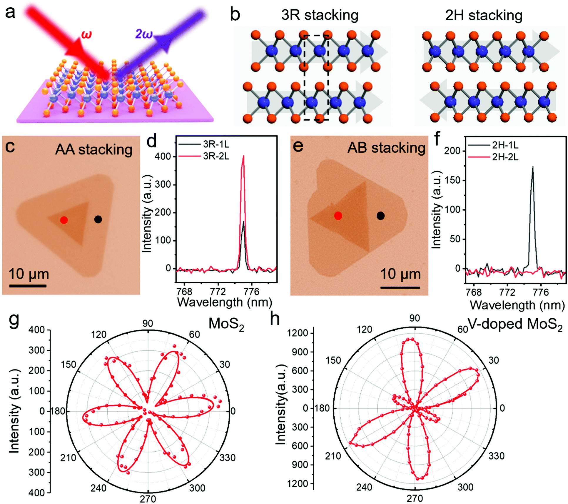 | ||
| Fig. 4 (a) Schematic diagram of SHG process. (b) Side view of bilayer 3R and 2H phase MoS2 with different stacking order. (c and e) Optical images of MoS2 with 3R and 2H stacking. (d and f) Layer number-dependent SHG response 3R and 2H phase V-doped MoS2. (g and h) Angular-dependent SHG intensity of monolayer MoS2 and V-doped MoS2. | ||
Polarization angle-dependent SHG was carried out to explore the crystalline structural characteristics. The monolayer MoS2 presents a typical six-fold symmetric pattern (Fig. 4(g)). However, the six-fold pattern of monolayer V-doped MoS2 was nonuniform shaped, with four folds enlarged compared with the two shrunken folds (Fig. 4(h)). Obviously, the situation changed with the doping of V atom in MoS2 lattice. We further measured the SHG response of bilayer V-doped MoS2 flakes with different stacking orders. Fig. 5(a) and (d) display the optical microscopy images of as-synthesized AA-stacking and AB-stacking V-doped MoS2 flakes. Their corresponding Raman spectra were given in Fig. S3.† Both AB-stacking and AA-stacking flakes grown on the uniform SiO2/Si substrate show consistent optical contrast, indicating they possess the same number of layers. AFM measurements were carried out to identify the thickness and layers, and the results of an AA-stacking flake demonstrate the center was bilayer (Fig. S4†). We characterized the SHG mapping (Fig. 5(b)) of a flake with bilayer AA-stacking in the center and monolayer in the edge, highlighted by red dashed box in Fig. 5(a). It is apparent that the center section presented stronger SHG response than the edge according to the image's contrast. The quantitative SHG intensities of 3R stack monolayer and bilayer are presented in Fig. 5(c). To our surprise, the bilayer AB-staking 2H phase flakes also generate a strong SHG signal (Fig. 5(e)) and the intensity is almost same as that from 3R bilayer (Fig. 5(f)), demonstrating a breakage of inverse symmetry in 2H phase V-doped MoS2. This was originally from the random distribution of V-substitute for Mo sites, which causes a slight lattice strain to break the symmetric structure.33
 | ||
| Fig. 5 SHG mapping of bilayer 3R and 2H phase V-doped MoS2. (a and d) Optical images of V-doped MoS2 with 3R and 2H stacking. (b and e) SHG intensity mapping of V-doped MoS2 flakes from (a and d), marked by red dashed boxes. (c and f) Layer number-dependent SHG response 3R and 2H phase V-doped MoS2. | ||
Conclusions
In summary, we synthesized the V-doped MoS2 flakes using V2O5 precursor via CVD method. The crystalline structure was determined by STEM characterization. SHG measurement was further used to investigate the inverse symmetry of 2H and 3R phase V-doped MoS2 with different stacking orders. The nearly consistent SHG response in bilayer 2H and 3R phase V-doped MoS2 indicated the broken inversion symmetry regardless of stacking order and layer numbers. The doping 2D crystal provides a profitable strategy to extend the range of atomically thin optical material with second-order nonlinearity.Conflicts of interest
There is no conflict to declare.Acknowledgements
This work is supported by National Key Research and Development Program of China (2020YFB2008501), the National Natural Science Foundation of China (11904289, 61775183), Key Research and Development Program of Shaanxi Province (2020ZDLGY04-08, 2020GXLH-Z-027), the Natural Science Foundation of Ningbo (202003N4003), the Fundamental Research Funds for the Central Universities (D5000210868, 3102019PY004, 31020190QD010, 3102019JC004), start-up funds from Northwestern Polytechnical University (19SH020159, 20GH020140).References
- S. Bertolazzi, J. Brivio and A. Kis, Stretching and Breaking of Ultrathin MoS2, ACS Nano, 2011, 5, 9703 CrossRef CAS PubMed.
- A. Castellanos-Gomez, M. Poot, G. A. Steele, H. S. J. van der Zant, N. Agraït and G. Rubio-Bollinger, Elastic Properties of Freely Suspended MoS2 Nanosheets, Adv. Mater., 2012, 24, 772 CrossRef CAS PubMed.
- K. Liu, Q. Yan, M. Chen, W. Fan, Y. Sun, J. Suh, D. Fu, S. Lee, J. Zhou, S. Tongay, J. Ji, J. B. Neaton and J. Wu, Elastic Properties of Chemical-Vapor-Deposited Monolayer MoS2, WS2, and Their Bilayer Heterostructures, Nano Lett., 2014, 14, 5097 CrossRef CAS PubMed.
- B. Radisavljevic, A. Radenovic, J. Brivio, V. Giacometti and A. Kis, Single-layer MoS2 transistors, Nat. Nanotechnol., 2011, 6, 147 CrossRef CAS PubMed.
- W. Wu, L. Wang, Y. Li, F. Zhang, L. Lin, S. Niu, D. Chenet, X. Zhang, Y. Hao, T. F. Heinz, J. Hone and Z. L. Wang, Piezoelectricity of single-atomic-layer MoS2 for energy conversion and piezotronics, Nature, 2014, 514, 470 CrossRef CAS PubMed.
- J.-H. Lee, J. Y. Park, E. B. Cho, T. Y. Kim, S. A. Han, T.-H. Kim, Y. Liu, S. K. Kim, C. J. Roh, H.-J. Yoon, H. Ryu, W. Seung, J. S. Lee, J. Lee and S.-W. Kim, Reliable Piezoelectricity in Bilayer WSe2 for Piezoelectric Nanogenerators, Adv. Mater., 2017, 29, 1606667 CrossRef PubMed.
- D. Hu, C. Ye, X. Wang, X. Zhao, L. Kang, J. Liu, R. Duan, X. Cao, Y. He, J. Hu, S. Li, Q. Zeng, Y. Deng, P.-F. Yin, A. Ariando, Y. Huang, H. Zhang, X. R. Wang and Z. Liu, Chemical Vapor Deposition of Superconducting FeTe1−xSex Nanosheets, Nano Lett., 2021, 21, 5338 CrossRef CAS PubMed.
- H. Wang, X. Huang, J. Lin, J. Cui, Y. Chen, C. Zhu, F. Liu, Q. Zeng, J. Zhou, P. Yu, X. Wang, H. He, S. H. Tsang, W. Gao, K. Suenaga, F. Ma, C. Yang, L. Lu, T. Yu, E. H. T. Teo, G. Liu and Z. Liu, High-quality monolayer superconductor NbSe2 grown by chemical vapour deposition, Nat. Commun., 2017, 8, 394 CrossRef PubMed.
- P.-F. Z. Mao-Sen Qin, X.-G. Ye, W.-Z. Xu, Z.-H. Song, J. Liang, K. Liu and Z.-M. Liao, Strain Tunable Berry Curvature Dipole, Orbital Magnetization and Nonlinear Hall Effect in WSe2 Monolayer, Chin. Phys. Lett., 2021, 38, 017301 CrossRef.
- X.-L. Li, W.-P. Han, J.-B. Wu, X.-F. Qiao, J. Zhang and P.-H. Tan, Layer-Number Dependent Optical Properties of 2D Materials and Their Application for Thickness Determination, Adv. Funct. Mater., 2017, 27, 1604468 CrossRef.
- Q. Hao, H. Yi, H. Su, B. Wei, Z. Wang, Z. Lao, Y. Chai, Z. Wang, C. Jin, J. Dai and W. Zhang, Phase Identification and Strong Second Harmonic Generation in Pure ε-InSe and Its Alloys, Nano Lett., 2019, 19, 2634 CrossRef CAS PubMed.
- M. Chhowalla, H. S. Shin, G. Eda, L.-J. Li, K. P. Loh and H. Zhang, The chemistry of two-dimensional layered transition metal dichalcogenide nanosheets, Nat. Chem., 2013, 5, 263 CrossRef PubMed.
- C. Tan, X. Cao, X.-J. Wu, Q. He, J. Yang, X. Zhang, J. Chen, W. Zhao, S. Han, G.-H. Nam, M. Sindoro and H. Zhang, Recent Advances in Ultrathin Two-Dimensional Nanomaterials, Chem. Rev., 2017, 117, 6225 CrossRef CAS PubMed.
- D. Yang, X. Hu, M. Zhuang, Y. Ding, S. Zhou, A. Li, Y. Yu, H. Li, Z. Luo, L. Gan and T. Zhai, Inversion Symmetry Broken 2D 3R-MoTe2, Adv. Funct. Mater., 2018, 28, 1800785 CrossRef.
- J. Chen, X. Zhao, G. Grinblat, Z. Chen, S. J. R. Tan, W. Fu, Z. Ding, I. Abdelwahab, Y. Li, D. Geng, Y. Liu, K. Leng, B. Liu, W. Liu, W. Tang, S. A. Maier, S. J. Pennycook and K. P. Loh, Homoepitaxial Growth of Large-Scale Highly Organized Transition Metal Dichalcogenide Patterns, Adv. Mater., 2018, 30, 1704674 CrossRef PubMed.
- J. Shi, P. Yu, F. Liu, P. He, R. Wang, L. Qin, J. Zhou, X. Li, J. Zhou, X. Sui, S. Zhang, Y. Zhang, Q. Zhang, T. C. Sum, X. Qiu, Z. Liu and X. Liu, 3R MoS2 with Broken Inversion Symmetry: A Promising Ultrathin Nonlinear Optical Device, Adv. Mater., 2017, 29, 1701486 CrossRef PubMed.
- Z. Zeng, X. Sun, D. Zhang, W. Zheng, X. Fan, M. He, T. Xu, L. Sun, X. Wang and A. Pan, Controlled Vapor Growth and Nonlinear Optical Applications of Large-Area 3R Phase WS2 and WSe2 Atomic Layers, Adv. Funct. Mater., 2019, 29, 1806874 CrossRef.
- Y. Song, R. Tian, J. Yang, R. Yin, J. Zhao and X. Gan, Second Harmonic Generation in Atomically Thin MoTe2, Adv. Opt. Mater., 2018, 6, 1701334 CrossRef.
- X. Fan, Y. Jiang, X. Zhuang, H. Liu, T. Xu, W. Zheng, P. Fan, H. Li, X. Wu, X. Zhu, Q. Zhang, H. Zhou, W. Hu, X. Wang, L. Sun, X. Duan and A. Pan, Broken Symmetry Induced Strong Nonlinear Optical Effects in Spiral WS2 Nanosheets, ACS Nano, 2017, 11, 4892 CrossRef CAS PubMed.
- C. T. Le, D. J. Clark, F. Ullah, J. I. Jang, V. Senthilkumar, Y. Sim, M.-J. Seong, K.-H. Chung, J. W. Kim, S. Park, S. H. Rhim, G. Kim and Y. S. Kim, Impact of Selenium Doping on Resonant Second-Harmonic Generation in Monolayer MoS2, ACS Photonics, 2017, 4, 38 CrossRef CAS.
- X. Fan, Z. Ji, R. Fei, W. Zheng, W. Liu, X. Zhu, S. Chen, L. Yang, H. Liu, A. Pan and R. Agarwal, Mechanism of Extreme Optical Nonlinearities in Spiral WS2 above the Bandgap, Nano Lett., 2020, 20, 2667 CrossRef CAS PubMed.
- K.-I. Lin, Y.-H. Ho, S.-B. Liu, J.-J. Ciou, B.-T. Huang, C. Chen, H.-C. Chang, C.-L. Tu and C.-H. Chen, Atom-Dependent Edge-Enhanced Second-Harmonic Generation on MoS2 Monolayers, Nano Lett., 2018, 18, 793 CrossRef CAS PubMed.
- E. Gürdal, A. Horneber, A. J. Meixner, D. P. Kern, D. Zhang and M. Fleischer, Enhancement of the second harmonic signal of nonlinear crystals by a single metal nanoantenna, Nanoscale, 2020, 12, 23105 RSC.
- H. Yu, D. Talukdar, W. Xu, J. B. Khurgin and Q. Xiong, Charge-Induced Second-Harmonic Generation in Bilayer WSe2, Nano Lett., 2015, 15, 5653 CrossRef CAS PubMed.
- Y. Wang, J. Xiao, H. Zhu, Y. Li, Y. Alsaid, K. Y. Fong, Y. Zhou, S. Wang, W. Shi, Y. Wang, A. Zettl, E. J. Reed and X. Zhang, Structural phase transition in monolayer MoTe2 driven by electrostatic doping, Nature, 2017, 550, 487 CrossRef CAS PubMed.
- T. Jiang, H. Liu, D. Huang, S. Zhang, Y. Li, X. Gong, Y.-R. Shen, W.-T. Liu and S. Wu, Valley and band structure engineering of folded MoS2 bilayers, Nat. Nanotechnol., 2014, 9, 825 CrossRef CAS PubMed.
- W.-T. Hsu, Z.-A. Zhao, L.-J. Li, C.-H. Chen, M.-H. Chiu, P.-S. Chang, Y.-C. Chou and W.-H. Chang, Second Harmonic Generation from Artificially Stacked Transition Metal Dichalcogenide Twisted Bilayers, ACS Nano, 2014, 8, 2951 CrossRef CAS PubMed.
- X. Zhang, H. Nan, S. Xiao, X. Wan, X. Gu, A. Du, Z. Ni and K. Ostrikov, Transition metal dichalcogenides bilayer single crystals by reverse-flow chemical vapor epitaxy, Nat. Commun., 2019, 10, 598 CrossRef CAS PubMed.
- L. Zhang, G. Wang, Y. Zhang, Z. Cao, Y. Wang, T. Cao, C. Wang, B. Cheng, W. Zhang, X. Wan, J. Lin, S.-J. Liang and F. Miao, Tuning Electrical Conductance in Bilayer MoS2 through Defect-Mediated Interlayer Chemical Bonding, ACS Nano, 2020, 14, 10265 CrossRef CAS PubMed.
- J. Zou, Z. Cai, Y. Lai, J. Tan, R. Zhang, S. Feng, G. Wang, J. Lin, B. Liu and H.-M. Cheng, Doping Concentration Modulation in Vanadium-Doped Monolayer Molybdenum Disulfide for Synaptic Transistors, ACS Nano, 2021, 15, 7340 CrossRef CAS PubMed.
- B. Tang, J. Zhou, P. Sun, X. Wang, L. Bai, J. Dan, J. Yang, K. Zhou, X. Zhao, S. J. Pennycook and Z. Liu, Phase-Controlled Synthesis of Monolayer Ternary Telluride with a Random Local Displacement of Tellurium Atoms, Adv. Mater., 2019, 31, 1900862 CrossRef PubMed.
- Q. Deng, X. Li, H. Si, J. Hong, S. Wang, Q. Feng, C.-X. Hu, S. Wang, H.-L. Zhang, K. Suenaga and H. Xu, Strong Band Bowing Effects and Distinctive Optoelectronic Properties of 2H and 1T′ Phase-Tunable MoxRe1−xS2 Alloys, Adv. Funct. Mater., 2020, 30, 2003264 CrossRef CAS.
- X. Ma, J. Zhang, J. Lai, M. Zhang, J. Zheng, S. Wu, X. Hu, Q. Wang, X. Gan, D. Sun and J. Liu, Gradient rhenium doping enabled tunable anisotropic valleytronic material based on monolayer molybdenum disulfide, 2D Mater., 2021, 8, 035031 CrossRef.
- R. Kappera, D. Voiry, S. E. Yalcin, B. Branch, G. Gupta, A. D. Mohite and M. Chhowalla, Phase-engineered low-resistance contacts for ultrathin MoS2 transistors, Nat. Mater., 2014, 13, 1128 CrossRef CAS PubMed.
- H. Yang, A. Giri, S. Moon, S. Shin, J.-M. Myoung and U. Jeong, Highly Scalable Synthesis of MoS2 Thin Films with Precise Thickness Control via Polymer-Assisted Deposition, Chem. Mater., 2017, 29, 5772 CrossRef CAS.
- J. Su, M. Wang, Y. Li, F. Wang, Q. Chen, P. Luo, J. Han, S. Wang, H. Li and T. Zhai, Sub-Millimeter-Scale Monolayer p-Type H-Phase VS2, Adv. Funct. Mater., 2020, 30, 2000240 CrossRef CAS.
- J. Zhou, J. Lin, X. Huang, Y. Zhou, Y. Chen, J. Xia, H. Wang, Y. Xie, H. Yu, J. Lei, D. Wu, F. Liu, Q. Fu, Q. Zeng, C.-H. Hsu, C. Yang, L. Lu, T. Yu, Z. Shen, H. Lin, B. I. Yakobson, Q. Liu, K. Suenaga, G. Liu and Z. Liu, A library of atomically thin metal chalcogenides, Nature, 2018, 556, 355 CrossRef CAS PubMed.
- X. Zhou, J. Cheng, Y. Zhou, T. Cao, H. Hong, Z. Liao, S. Wu, H. Peng, K. Liu and D. Yu, Strong Second-Harmonic Generation in Atomic Layered GaSe, J. Am. Chem. Soc., 2015, 137, 7994 CrossRef CAS PubMed.
- L. M. Malard, T. V. Alencar, A. P. M. Barboza, K. F. Mak and A. M. de Paula, Observation of intense second harmonic generation from MoS2 atomic crystals, Phys. Rev. B: Condens. Matter Mater. Phys., 2013, 87, 201401 CrossRef.
Footnotes |
| † Electronic supplementary information (ESI) available. See DOI: 10.1039/d1nr05725a |
| ‡ These authors contribute equal to this work. |
| This journal is © The Royal Society of Chemistry 2021 |