
 Open Access Article
 This Open Access Article is licensed under a
 Creative Commons Attribution 3.0 Unported Licence
MEMS-compatible, gold nanoisland anchored 1D aligned ZnO heterojunction nanofibers: unveiling the NO2 sensing mechanism with operando photoluminescence studies†
Ramakrishnan
Vishnuraj
,
Jayaseelan
Dhakshinamoorthy
,
Keerthi G.
Nair
,
Mahaboobbatcha
Aleem
and
Biji
Pullithadathil
 *
*
Nanosensor Laboratory, PSG Institute of Advanced Studies, Coimbatore – 641 004, India. E-mail: bijuja123@yahoo.co.in; pbm@psgias.ac.in
First published on 9th March 2021
Abstract
Production and alignment of heterojunction metal oxide semiconductor nanomaterial-based sensing elements for microsensor devices have always posed fabrication challenges since they involve multi-step synthesis processes. Herein, we demonstrate a coaxial electrospinning with an in situ photoreduction process for the fabrication of MEMS-compatible, 1D aligned gold nanoisland (GNI) anchored ZnO-based Heterojunction Nanofibers (HNFs) and their complex plasmon-mediated NO2 gas sensing mechanism has been investigated using operando photoluminescence studies. Evaluation of the gas sensing properties of aligned ZnO-GNI HNFs has exhibited excellent sensor response (196%) with rapid response time towards 500 ppb NO2 gas at reduced operating temperature (200 °C). Operando studies using photoluminescence and electrical measurements ascertained the existence of supplementary active sites in the multicrystalline nanofibers owing to the existence of Au nanograins over aligned ZnO nanofibers (NFs), thereby inducing a spill-over zone and aiding the charge transfer phenomenon. The operando PL studies also revealed the plasmonic effect of metallic Au and the role of zinc interstitial (Zni) defects and oxygen vacancies (V+o), which influence the charge transfer between ZnO and surface anchored Au nanoislands. This study revealed atomistic insights into the structural defects and charge transport properties of metal oxide semiconductor heterojunction materials, and the coaxial integration method of 1D aligned ZnO-GNI HNFs paves the way for unique strategies and the development of suitable MEMS based gas sensors for real-time applications.
1. Introduction
Metal oxide semiconductor (MOS) based heterojunction nanostructures have been extensively used for a wide range of fascinating applications in the emerging fields of oxidation catalysis,1 photocatalytic degradation,2 CO oxidation,3 photoelectrochemical water splitting,4 toxic gas detection5etc. Among various heterojunction materials, MOSs with plasmon mediated interfacial catalytic properties due to surface anchored noble metal nanoclusters have shown excellent sensing properties, especially towards the detection of oxidizing gases, like NO2.6 The plasmonic effect at the MOS heterojunctions has found to induce charge carrier excitation followed by carrier migration to the semiconductor and also increases the separation of charge recombination through the charge-transfer process.7 The effect of surface plasmon resonance associated with noble metal nanoclusters when supported on semiconductor nanostructures opens up new pathways for detecting toxic gases, such as NO2, which has become a serious environmental pollutant and major threat to human health.Among various MOS materials, quantum confined ZnO based one dimensional (1D) nanostructures, such as nanorods, nanowires, nanofibers, etc. have received huge attention in recent years towards the development of advanced devices owing to their directed electron transport properties.8 1D heterojunction nanomaterials based on ZnO could be an appropriate tool for the development of NO2 gas sensors. While the catalytic behaviour promote the spill-over effect and localized surface plasmon resonance (LSPR) originating from noble metal nanoislands anchored on 1D ZnO nanofibers can effectively enhance the NO2 sensing properties, it can also further trigger its performance owing to its 1D structure. Although a number of literature reports have endeavoured to explore the complex sensing mechanism in such heterojunction materials, more detailed analysis has not yet been reported. Furthermore, to explore the detection mechanism of pure MOS towards various gas analytes, Raman spectroscopy,9,10 Diffuse Reflectance Infrared Fourier Transform,11 X-ray Photoelectron Spectroscopy,12,13 UV-Visible Diffuse Reflectance spectroscopy,14 Electron Paramagnetic Resonance,15,16etc. have been employed as effective operando and in situ methods. Among various operando techniques, photoluminescence (PL) spectroscopy is found to be a unique approach, which can simultaneously deliver information about the recombination dynamics of the charge transfer phenomenon and defect emission ascribed to the recombination in various defect states involved in enhancing the gas adsorption.17–19 However, until now, real time studies based on PL spectral analysis to explore the sensing mechanism are limited to pure MOS materials towards various gas analytes.20–23 Recently, Li et al. described an ex situ photoluminescence study to reveal the sensing mechanism of a spinel type ZnFe2O4 based NO2 sensor and attempted to understand the oxygen vacancy-mediated charge transfer process.17 Cho et al. performed in situ PL analysis for 2D MoS2 to elucidate the electron transfer mechanism during NO2 gas adsorption. The electron depletion of MoS2 by NO2 adsorption was found to lead to enhanced intensity of the A+ peak and a quenching of the A0 peak pointing towards the nature of electron transfer among MoS2 and NO2 molecules.19 Similarly, Ou et al. observed strongly quenched PL of SnS2 upon exposure to NO2 thereby predicting the electron transfer mechanism.23 It is noteworthy that no reports exist on operando PL studies for unveiling the complex gas sensing mechanism of heterojunction MOS materials under operational conditions.
On the other hand, while considering MOS based heterojunction nanostructures as suitable materials for current sensor industries, the multi-step synthetic processes impede their wider use.24 Although wet-chemically synthesized heterojunction MOS based 1D nanorods or nanowires offer high charge transport properties, integration of such wet-chemically synthesized materials often found issues during fabrication like device-to-device inconsistency and integration issues during device fabrication.25 Many researchers have attempted to develop on-chip fabrication of sensor devices and such methods are either based on pristine MOS materials or composites, which involve multi stage processes hindering their device integration.26–29 Such issues can be addressed by adopting single-step production methods for the on-chip fabrication of MOS heterojunction nanofibers with controlled surface doping of catalytic metals/metal oxides. Among various synthetic methods, electrospinning is a versatile technique used for the fabrication of MOS nanofibers. In particular, on-chip fabrication of MOS HNFs can be easily accomplished using coaxial electrospinning with effective control over the orientation of 1D nanofibers and eliminates solvent and impurity effects during wet-chemical synthesis of MOS heterojunction materials. This study focuses on a facile single-step fabrication process of 1D aligned coaxial heterojunction metal oxide semiconductor nanofiber (with ZnO/Au as a model nanosystem) based microsensor devices, which have always posed fabrication challenges, since existing methodologies involve multi-step synthetic processes. Coaxial electrospinning of nanofibers can also allow suitable functionalization of metal/metal oxide nanofibers and permit proper alignment of nanofibers on the active area of the sensor device. To date, direct on-chip fabrication of aligned MOS based heterojunction nanofibers using coaxial electrospinning for NO2 sensor applications has not yet been reported.
In this investigation, we have developed one dimensionally aligned ZnO-GNI nanofibers as a model heterojunction nanosystem, where the effect of catalytic sensitization and structural orientation can be easily achieved to understand their complex sensing mechanism that affects the sensor device performance. A novel synthetic approach based on coaxial electrospinning coupled with in situ photoreduction has been developed for the direct on-chip fabrication of 1D aligned core–shell heterojunction MOS nanofibers, which is otherwise a tedious multistep process. Investigation of the surface catalysis associated with the noble metal cluster (Au) anchored on ZnO nanofibers by analyzing gas/material interactions occurring at the heterojunction interfaces can also lead to a holistic understanding of the sensing mechanism which was further verified by in situ spectroscopic and crystallographic investigations. NO2 gas sensing calibration of aligned ZnO-GNI nanofibers revealed an excellent sensitivity, high selectivity and fast response/recovery time towards the trace level concentration of NO2. Moreover, in order to reveal the charge transport and role of surface defects and oxygen vacancies associated with heterojunction nanostructures, operando PL analysis coupled with electrical measurements were performed. The NBE emission with deep level defects observed under operational conditions explored the surface band bending phenomenon associated with the heterojunctions that can aid in understanding the complex detection mechanism of aligned ZnO-GNI HNF based sensors at reduced working temperature. To the best of our knowledge, this is the first report on on-chip, single step fabrication of aligned ZnO-GNI HNFs for NO2 gas sensor application and operando PL spectral analysis during electrical characteristics acquisition. This investigation can contribute greatly to the choice of better sensing materials and processing conditions for sensor device fabrication and can pave the way for the development of low-cost aligned single nanowire devices with improved selectivity.
2. Experimental section
Materials: zinc acetate (Zn(CH3COO)2·2H2O, 98%, Merck), gold chloride (HAuCl4, 99.99%), polyvinyl alcohol (PVA-1![[thin space (1/6-em)]](https://www.rsc.org/images/entities/char_2009.gif) 400000), and polyvinyl pyrrolidone (PVP-200000) were purchased from Sigma Aldrich chemicals. Ultrapure water (Millipore, resistivity – 18.2 MΩ cm) was used for all the experiments.
400000), and polyvinyl pyrrolidone (PVP-200000) were purchased from Sigma Aldrich chemicals. Ultrapure water (Millipore, resistivity – 18.2 MΩ cm) was used for all the experiments.
2.1 Co-axial electrospinning of 1D aligned ZnO-GNI nanofibers
Aligned ZnO-GNI HNFs were fabricated using a coaxial electrospinning technique. Experimental set-up used for coaxial electrospinning consisted of a high voltage DC power supply, dual syringe pump, coaxial spinneret and copper collector. The inner feed solution, a zinc acetate/PVA mixture, was prepared as a homogeneous solution (A). While preparing the outer feed solution, 2.5 mM HAuCl4·nH2O was added to 10 mL of ultrapure water and subjected to stirring for 1 h. 8 wt% of polyvinyl pyrrolidone (PVP) was added to this solution to prepare the outer feed solution (B). The precursor solutions A and B were loaded in two 10 mL syringes, connected to a Teflon coaxial spinneret. Both feed solutions were subjected to simultaneous electrospinning at a voltage, 20 kV with needle-collector distance of 22 cm using an independently controlled dual syringe pump. The flow rates were set as 0.5 mL h−1 and 0.8 mL h−1 for outer and inner fluids respectively. During the electrospinning process, the spinning space was exposed to UV radiation (λ = 254 nm) to facilitate in situ photoreduction of Au3+ present in the outer shell layer to form Au(0) nanoclusters to form heterojunctions on the inner core ZnO nanofibers. The electrospun Zn(CH)3COO2/PVA@Au(0)/PVP nanofibers were annealed at 550 °C for 4 h in a tubular furnace at the rate of 4 °C min−1 to remove the organic matter and to form crystalline ZnO-GNI HNFs on IDA transducers. For production of aligned ZnO-GNI HNFs, the electrospinning process was attempted using gold sputtered interdigitated array (IDA) electrodes with an interfinger gap of 80 μm and an overall sensing area of 18 mm2 as the collector plate. The parallel collector geometries associated with the IDA fingers assisted in alignment of the nanofibers across the finger electrodes.2.2 Fabrication of coaxial spinneret assembly and coaxial electrospinning with in situ UV-irradiation
An in-house electrospinning unit with in situ ultraviolet (UV) irradiation facility was designed and developed for a coaxial electrospinning process as shown in Fig. S1(a) (ESI†). For the production of core–shell HNFs, noble-metal nanoclusters constituted the shell layer, which was produced using in situ photo reduction by UV-irradiation of the electrospun fibers. The high voltage power supply of 30 kV was used for the electrospinning unit with a Glassman system. In order to synthesise core–shell nanofibers, coaxial spinneret components were designed using AutoCAD (Fig. S1b, ESI†) and fabricated using Teflon as depicted in Fig. S1(c and d) (ESI†).2.3 Operando PL studies
Operando photoluminescence emission studies were performed to explore the defect-mediated NO2 sensing mechanism of ZnO-GNI heterojunction nanosystems through their unique near band edge (NBE) emission characteristics and defect level emission behaviour during gas/material interactions. PL spectra were acquired using Confocal Raman Microscope (WITec alpha 300R, Germany) with an excitation monochromatic laser source at 355 nm with 1800 g mm−1 gratings in the backscattering arrangement. The spectra were acquired in the wavelength range of 350 to 750 nm. Emission spectra were collected in the backscattering geometry through a 20× objective lens during the gas/material interactions at the sensor operating conditions. LINKAM probe station (HFS600E-PB4) equipped with a temperature-dependent heating stage capable of varying temperature up to 600 °C was used to examine the operando emission properties under working conditions. The NO2 gas flow rate was maintained constant at 100 sccm under dynamic conditions with N2 as the carrier gas.3. Results and discussion
1D aligned ZnO-GNI HNFs were developed using a direct, on-chip fabrication method using coaxial electrospinning with in situ photo reduction followed by thermal treatment at 550 °C as shown in Fig. 2(a). The unidirectional alignment of nanofibers between the IDA electrode fingers was initially simulated using a finite element method (FEM), which was used to analyse the 3D distribution of electric field lines during the electrospinning process. The real dimensions, needle-collector distance, environmental conditions and material properties of IDA electrode, parallel plate collector and needle diameter were used as the physical geometry parameters. High electric potential is the core constraint focused on in this study. The parallel plate collector was placed at 180 mm distance from the needle and the collector sheet size was set as 30 mm × 30 mm. The syringe tip was biased at a high DC voltage of 20 kV with reference to the grounded collector sheet. Electric field simulation of the electrospinning process was performed using the COMSOL Multiphysics package as presented in Fig. 1(a and b). The grid independent study was conducted based on electric field simulation of a 3D electrospinning model with 477857 mesh elements, which gave the optimum solution. The mesh statistics data are given in Table S1 (ESI†). Fig. 1(c) shows the contour figure of the electric field line distribution among the needle tip and the parallel plate electrodes. The intensity of electric field was found to be intense at the tip of the nozzle which is clearly evident in the contour diagram and gradually diminished with an increase in the nozzle to collector distance. Fig. 1(d) shows the electric field lines formed between the Cu parallel plate collectors.30 The electric field distribution on the Au IDA electrode placed between the Cu parallel plate collectors is depicted in Fig. 1(d), which further confirmed that the simple parallel plate collectors can induce effective alignment of nanofibers across the IDA finger electrodes without any secondary electric field.31,32 Based on the simulations, aligned ZnO-GNI HNF based NO2 sensor devices were fabricated by directly electrospinning using coaxial spinneret. Au sputtered IDA transducer electrode was placed between two copper parallel plate collectors to acquire appropriate alignment of nanofibers between the IDA fingers and to eliminate the ancillary potential as depicted in Fig. 2(a). An 8 W–254 nm UV source was used for in situ photoreduction with an electrospinning process, which was illuminated between the needle and collector and induced reduction of Au3+ to Au0 and the agglomeration of Au nanoclusters during thermal decomposition of polymeric contaminants was eliminated.33 The alignment of nanofibers was carried out using Au sputtered IDA electrode and the overall coaxial electrospinning process was performed inside a dark enclosure. The nanofibers were aligned across the IDA fingers following the electric field lines as predicted by simulations. Thus, the Au nanoparticles decorated ZnO HNFs could be directly aligned on the IDA sensor device.
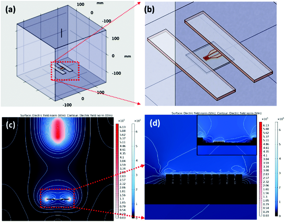 | ||
| Fig. 1 (a and b) 3D representation of electrospinning assembly with parallel plate collector, (c) illustration of contour distribution of electric lines among needle tip and collector and between the IDA electrodes and (d) depiction of electric field line distribution between the IDA electrodes placed in between the parallel plate collectors (inset shows electric field line distribution between parallel plate collectors). | ||
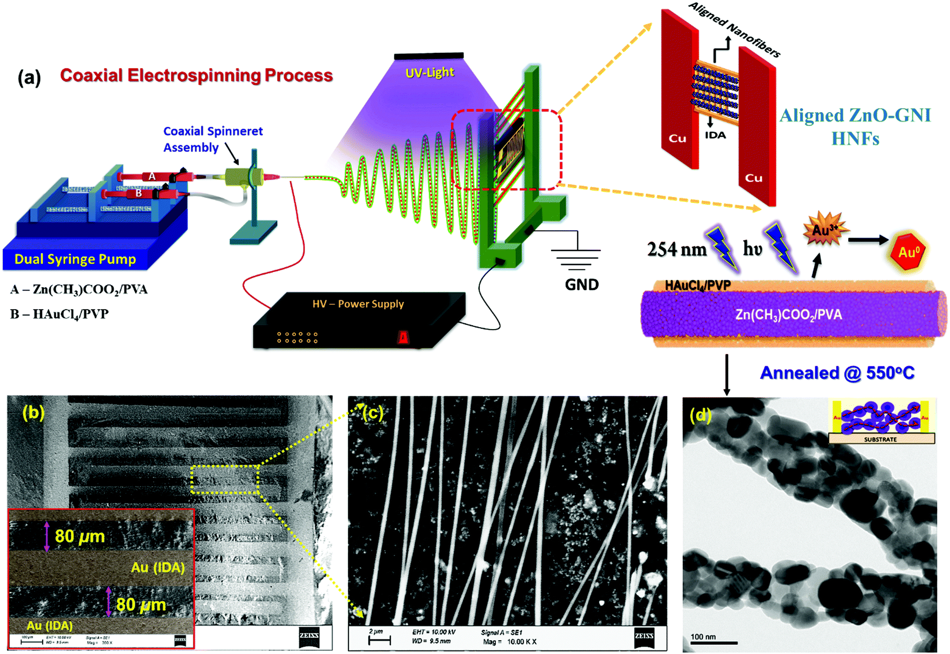 | ||
| Fig. 2 (a) Schematic representation of on-chip fabrication of aligned ZnO-GNI HNFs by coaxial electrospinning process with in situ photoreduction. (b and c) SEM image of electrospun aligned nanofibers deposited on Au sputtered IDA electrode and (d) TEM image of annealed ZnO-GNI nanofibers. | ||
Fig. 2(b and c) depict the SEM images of the fabricated aligned ZnO-GNI nanofibers on an IDA electrode before thermal treatment. The as-spun nanofibers were found to be highly aligned and with several micro-meter length and high aspect ratio applicable for electronics-sensing applications. As observed from the TEM image shown in Fig. 2(d), the ZnO-GNI nanofibers possessed nanograined morphology after a thermal treatment process and the relative grain size was estimated as 22 ± 5 nm with a typical fibre diameter of 90 ± 8 nm. This unique method can offer many advantages over the existing technologies for sensor fabrication, such as (i) the direct on-chip fabrication method of sensing materials on sensor devices using a cost-effective coaxial electrospinning process, (ii) offers a single-step method for fabrication of aligned HNFs with effective control over orientation of 1D nanofibers, (iii) eliminates solvent and impurity effects during wet-chemical synthesis of sensing materials, (iv) allows suitable functionalization of metal oxide nanofibers by coaxial nanofiber assembly, (v) reduced operating temperature with improved selectivity with the HNFs, (vi) provides a model platform for a holistic understanding of the gas/material interactions for unravelling the complex sensing mechanism, and (vii) it can pave the way to a low-cost method for single nanowire devices with improved selectivity.
3.1 Structural analysis of 1D ZnO-GNI nanofibers
XRD spectral analysis of pure ZnO and ZnO-GNI HNFs were performed to confirm the space lattice structure as depicted in Fig. 3(a).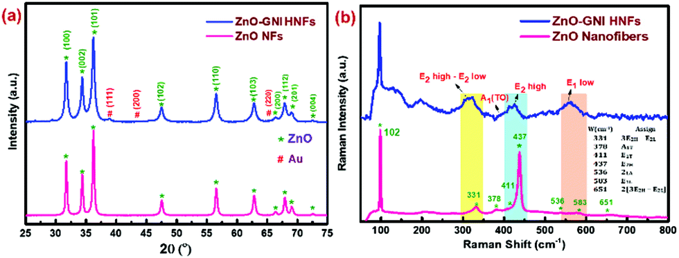 | ||
| Fig. 3 (a) X-ray diffraction spectra and (b) Raman shifts of pure ZnO nanofibers and ZnO-GNI HNFs. | ||
The intense diffraction peaks detected at 2θ resembles the respective lattice planes further correlated with the hexagonal wurtzite phase of pure ZnO as revealed in our previous report.34 In the case of ZnO-GNI HNFs, along with the characteristic peaks of ZnO, the 2θ peaks detected at 38.33 and 44.12 were recognized to be the fcc structure of Au with an existing lattice plane of (111) and (200) (JCPDS # 01–1174). Diffraction peaks corresponding to gold nanoislands and absence of peak shifts for hexagonal ZnO suggest the decoration of gold nanoislands which further confirmed the existence of heterojunctions in ZnO-GNI HNFs.35
Raman spectra of bare ZnO nanofibers and ZnO-GNI HNFs were recorded using a 532 nm laser in a backscattering approach as compared in Fig. 3(b). Raman spectra of 1D pristine ZnO nanofibers acquired at RT exhibited an intense peak observed at 437 cm−1 due to the E2high mode of the wurtzite phase of the ZnO nanostructure. The strong peak observed in the E2 mode confirms the crystallinity of ZnO. Moreover, additional peaks arising near minor frequency at 331 cm−1 and 377 cm−1 correspond to the phonon vibrations at the zone boundary, E2high − E2low and A1 (TO) modes respectively. Likewise, the peaks detected at 329 and 437 cm−1 could be attributed to the zone-boundary interactions of phonons in ZnO. Comparable Raman peaks of ZnO were detected for ZnO-GNI HNFs with considerable shift as depicted in Fig. 3b, owing to the existence of gold nanoislands anchored over the ZnO surface.36–38 A broad peak detected near 578 cm−1 related with the E1(LO) mode reflecting the prevalence of high oxygen vacancies (Vo) and zinc interstitials (Zni) in the materials. Pristine ZnO and ZnO-GNI HNFs showed a prominent E1(LO) band, which confirmed the existence of Vo and Zni defects. The formation of heterojunctions leads to interfacial charge transfer which was confirmed from the quenched E2high and E1(LO) bands with significant shift in peak as observed for ZnO-GNI HNFs which may enhance the NO2 sensing characteristics.39
3.2 Morphological characterization of ZnO-GNI nanofibers
TEM image analysis of porous ZnO-GNI HNFs is depicted in Fig. 4. ZnO-GNI nanofibers displayed a characteristic nanograined multicrystalline structure with one dimensional morphology as depicted in Fig. 4(a). Furthermore, it is evident from the high resolution TEM images of ZnO-GNI HNFs and the histogram (inset) in Fig. 4(b) that the average grain size of ZnO in ZnO-GNI HNFs is estimated as 22 ± 6 nm and the length extends to some micrometers through the high aspect ratio as appropriate to electronics and sensing applications. The average particle size of Au nanoparticles anchored on ZnO was calculated as 15 ± 2 nm (Fig. 4a and b). The SAED pattern of heterojunction nanofibers displayed concentric ring patterns of ZnO-GNI as depicted in Fig. 4(c) further confirming the multicrystalline nature of the nanoparticles corresponding to hexagonal ZnO and cubic Au owing to the formation nanograined morphology. The SAED pattern was further indexed and the (101), (203), (110) and (112) planes represent the wurtzite ZnO crystal lattice and the (111) and (311) planes correspond to the cubic Au crystal plane as inferred from the JCPDS card no. 36-1451 for ZnO and JCPDS card no. 04-0748 for Au respectively. The HRTEM image of ZnO-GNI nanofibers depicted in Fig. 4(d) evidently displays the presence of discrete lattice fringes for individual ZnO nanograins and Au nanoislands. Furthermore, in order to estimate the d-spacing values of ZnO-GNI, inverse FFT image processing was carried out using a digital micrograph package as described in Fig. S11(a and b) (ESI†). The inter-planar spacing of ZnO was measured as 2.81 Å, which corresponds to the [100] lattice and 2.41 Å of the Au nanoisland is related to the [111] lattice as revealed in Fig. S11(c and d) (ESI†). The results further confirmed the formation of ZnO-GNI heterojunctions at the interfaces.40 Moreover, the ZnO-GNI HNFs exhibited nanograined morphology with intrinsic porosity formed during the calcination process coupled with abundant surface area, which could emboss the ZnO-GNI HNFs as efficient sensing materials at reduced operating temperature. Furthermore, BET analysis was carried out to quantify the specific surface area and analyze the porous structure of ZnO-GNI HNFs. Detailed BET surface area analysis of ZnO nanofibers and porous ZnO-GNI nanofibers are depicted in Fig. S12 (ESI†) and the calculated BET surface area, pore volume and pore size are summarized in Table S6 (ESI†). The increase in specific surface area of 26.688 m2 g−1 and pore volume of 0.092 cm3 g−1 for ZnO-GNI HNFs compared to pristine ZnO nanofibers can provide abundant surface-active sites and facilitate the easy charge-carrier transport leading to enhanced NO2 sensing properties.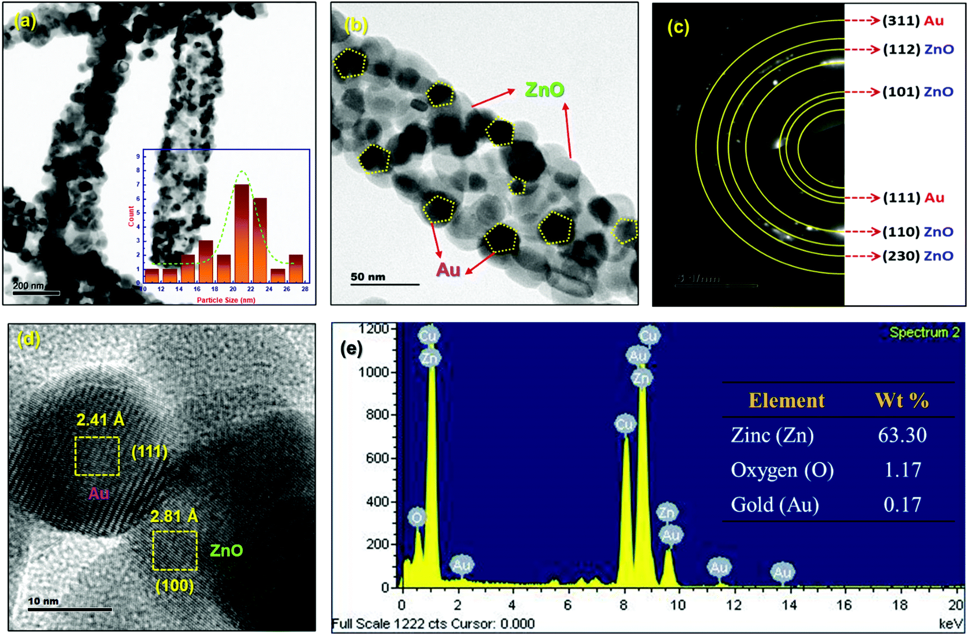 | ||
| Fig. 4 (a and b) TEM images of ZnO-GNI HNFs, (c) corresponding SAED pattern of ZnO-GNI nanofibers, (d) HRTEM image of ZnO-GNI nanofibers and (e) EDX spectra of ZnO-GNI nanofibers. | ||
3.3 XPS analysis of ZnO-GNI nanofibers
The XPS analysis was conducted to examine the oxidation states of the chemical elements present in ZnO-GNI HNFs. Fig. 5(a) displays the survey scan spectra of pristine ZnO and ZnO-GNI nanofibers which revealed the existence of peaks consistent to zinc, gold and oxygen confirming the material purity. Fig. 5(b) depicts the fine-scan Zn 2p peaks of pure ZnO and ZnO-GNI ZnO-GNI HNFs. Fine scan Zn 2p peaks exhibited major binary peaks detected at a binding energy value of 1044.5 eV and 1021.5 eV consistent with Zn 2p1/2 and Zn 2p3/2 respectively, which indicates the divalent oxidation state of ZnO. Furthermore, energy separation between these two peaks is 23.0 eV which confirms the existence of a Zn2+ state in the ZnO crystal plane in nanofibers.41 However, ZnO-GNI HNFs exhibited a chemical shift to a lower binding energy of 1020.4 and 1043.4 eV, associated with pure ZnO nanofibers due to accommodation of Au nanoislands over the surface of ZnO and existence of Zni defects in the nanograined structure. The fine scan analysis of the O1s spectrum of ZnO-GNI nano fibers is depicted in Fig. 5(c). The O1s bands in pristine ZnO and ZnO-GNI nanofibers were deconvoluted into two peaks corresponding to OI and OII; the peak at 528.8 eV is assigned to lattice oxygen species existing in Zn–O bonding and the peak at 530.4 eV is related to the oxygen-deficient region (O− and O2− ions) in the fibre network.42 | ||
| Fig. 5 (a) Survey scan XPS spectrum and high-resolution peaks of (b) Zn 2p, (c) O 1s, and (d) Au 4f corresponding to pristine ZnO and ZnO-GNI HNFs. (e) Valence band onset region of UPS spectra of pure ZnO NFs and ZnO-GNI HNFs and (f) secondary edge region. | ||
As inferred from Fig. 5(c), the binding energy peak is attributed to OIIi.e., chemisorbed oxygen species which was found to be dominant in ZnO-GNI nanofibers owing to the existence of more nanograins, that can be further correlated with the sensing phenomenon. The O1s peak in the ZnO-GNI HNFs was found to shift to lower binding energy compared to pristine ZnO nanofibers owing to the existence of gold nanoislands that accept electrons from the surface of ZnO at the heterojunctions and thereby create oxygen vacancies.42–44 Hence, oxygen vacancies induce a lower energy shift of O 1s peak. Consequently, the occurrence of surface-active sites and enhanced catalytic behaviour of Au nanoislands at the heterojunctions can make them an active sensing material. Fig. 5(d) shows the fine scan spectra of Au 4f and Zn 3p peaks in ZnO-GNI nanofibers.
The high-resolution Au 4f peak of ZnO-GNI nanofibers was found to be overlayed with Zn 3p of ZnO, which was further deconvoluted to corresponding peaks related to Au 4f7/2 (81.7 eV), Au 4f5/2 (85.3 eV), Zn 3p3/2 (86.9 eV) and Zn 3p1/2 (89.6 eV), respectively, as depicted in Fig. 5d. Moreover, the absence of an Au 4f signal in the pure ZnO nanofibers was clearly evident in the high-resolution Zn 3p spectra. This indicates the distribution of Au nanoislands formed on ZnO nanofibers during coaxial spinning followed by thermal treatment.43 However, ZnO-GNI nanofibers showed characteristic nanograined morphology and randomly oriented Au nanoislands, the conduction band of ZnO is nearly equivalent to the Fermi level of Au, so that the electron can transfer from ZnO to Au producing higher electron density on at the surface anchored Au nanoislands. These findings can be further affirmed with the operando PL spectral studies performed under the sensor operational conditions. Such intricate analysis can also unveil the electron transfer phenomenon and intrinsic defects present in the ZnO-GNI HNFs which can significantly enhance the NO2 gas sensing characteristics. Furthermore, the valence band onset (Eon-set) and secondary electron cut-off (Ecut-off) of pure ZnO NFs and ZnO-GNI HNFs are shown in the Fig. 5(e and f). As observed from the UPS spectra, Eonset and Ecutoff was calculated to be 2.39 and 2.22 eV and 15.6 and 16.8 eV, respectively. Using the incident energy, hν = 21.2 eV (He1 laser source), the work functions of pristine ZnO NFs and ZnO-GNI HNFs have been estimated as 5.2 eV and 4.5 eV respectively. The gold nanoisland anchored ZnO nanofibers show reduction in the work function owing to the formation of a Schottky contact which further leads to easy electron transfer from ZnO to Au.
3.4 Aligned ZnO-GNI nanofiber based NO2 gas sensor calibration
The NO2 sensing characteristics of aligned ZnO-GNI HNFs fabricated onto an IDA transducer electrode were evaluated using the gas sensor calibration unit existing in our laboratory.45 The NO2 sensing properties of ZnO–Au nanosystems were assessed using a custom-built gas sensor test station. The details of the gas sensor calibration unit have been given in the ESI† (Section S4). The working temperature of gas sensors is one of the important parameters which has a considerable impact on sensitivity and selectivity. Fig. 6(a) shows the sensor response of bare and 1D aligned ZnO-GNI HNFs towards exposure to 1 ppm of NO2 gas at varied temperature (50–350 °C). The highest sensitivity (S) was observed at 300 °C and 200 °C for ZnO nanofibers (193%) and aligned ZnO-GNI HNFs (462%) respectively, toward NO2 gas, which were further selected as the operating temperatures. It was revealed that the operating temperature was decreased for aligned ZnO-GNI HNFs compared to pure ZnO nanofibers. The current study reveals that aligned ZnO-GNI nanofibers based sensor exhibited reduced working temperature and boosted the response towards NO2 compared to pristine ZnO owing to the presence of catalytic Au nanoislands upon physisorption of analyte gas. For pristine ZnO nanofibers, higher operating temperature induces a greater number of O− ions on the ZnO surface and thereby the rate of NO2 adsorption was found to be increased. In the case of aligned ZnO-GNI nanofibers, owing to the difference in the workfunction of ZnO and Au, electrons transfer from ZnO to the Au site and therefore the catalytic Au nanoislands become electron rich active centers. Therefore, during NO2 exposure, excess electrons present in the Au nanoislands can be easily captured by the oxidizing NO2 molecules at reduced temperature and spill-over effect leading to further surface reactions with surrounding ionosorbed oxide ions on ZnO. This could further promote the formation of depletion region near the heterojunctions on the surface of ZnO-GNI nanofibers.36 Hence, the energy needed to achieve maximum sensor response is significantly less for ZnO-GNI nanofibers than pristine ZnO nanofibers.46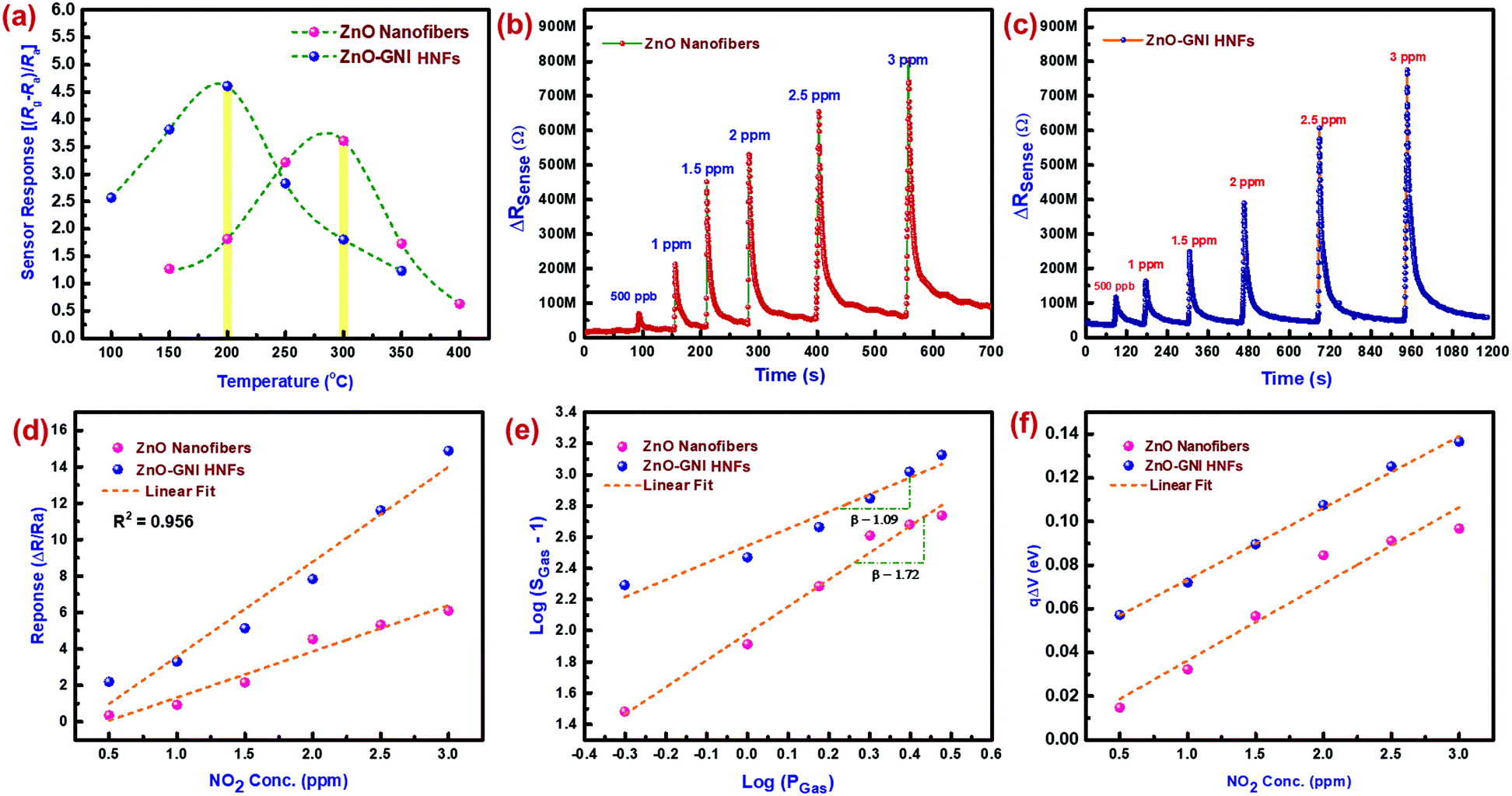 | ||
| Fig. 6 (a) Sensor response graph of NO2versus different temperature, (b and c) NO2 sensor response–recovery plots of pristine ZnO and aligned heterojunction ZnO-GNI HNFs at its operational temperature, (d) sensor response against NO2 concentration, (e) log(Sgas − 1) versus log(Pgas) plot toward 0.5–3 ppm of NO2 gas and (f) effect of band bending upon increasing NO2 concentration. | ||
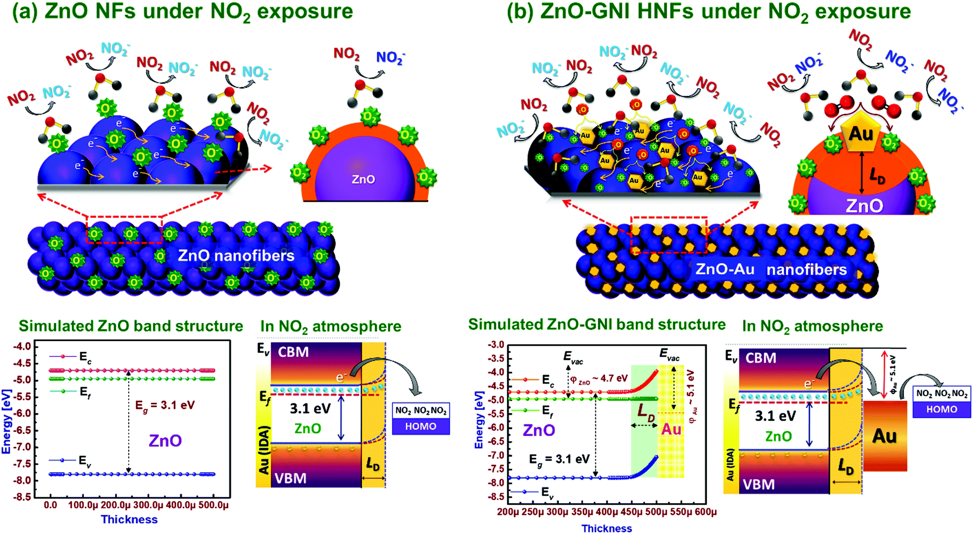
The electronic sensitization takes place when NO2 species adsorb on the core ZnO nanograined fibre and spill-over from the catalytic Au nanocluster to ZnO. The change in resistance occurs during the surface reaction of NO2 with the chemisorbed negative ions existing over the ZnO surface. Fig. 6(b and c) depicts the dynamic sensor response/recovery plots for pristine ZnO and aligned ZnO-GNI nanofibers at different NO2 concentrations at an ideal operating temperature. With an increase in NO2 gas concentration, variation of resistance was found to be correspondingly increased. Fig. 6(d) depicts the comparative sensor response (ΔR/Ra) as a function of NO2 concentration ranging from 500 ppb to 3 ppm which was tailed to be in the linear trend. The NO2 sensor parameters are tabulated in Table S3 (ESI†). The NO2 sensing properties depicted in Table S3 (ESI†) show that the sensitivity increased from ∼32% to ∼196% towards exposure to 500 ppb of NO2 gas for pristine ZnO and aligned ZnO-GNI nanofibers respectively with a fast response time (tres(90)) of 4–5 s compared to that of pristine ZnO nanofibers with a response time (tresp(90)) of 7–10 s. However, 1D aligned ZnO-GNI HNF based sensors possess a lower detection limit (LOD) of 500 ppb which is an important index of gas sensor performance as depicted in Fig. S13 (ESI†). The enhanced sensitivity of heterojunction nanofibers can be ascribed to the directed electron transfer via radial conduction process through 1D ZnO nanofiber and the charge transfer at the Au–ZnO interfaces. Also, highly aligned nanofibers oriented across the IDA fingers and co-existence of intrinsic defects in the nanograined heterojunction fibers lead to higher NO2 adsorption compared to pristine nanofibers.
While exposing the heterojunction nanofibers to NO2 atmosphere, the NO2 gas species primarily interact with chemisorbed O− and minor O2− species, and further trap additional carriers from the higher state instead of interacting directly on the ZnO surface. Therefore, the resistance increases by reducing the electron accumulation region (LD) of the heterojunction interface. In order to ascertain the nature of the adsorbed oxygen species on ZnO-GNI HNFs, the slope of log(SGas − 1) against log(PGas) was estimated from Fig. 5(e). Typically, the exponent β expressed in the relation (S = aCβ) is the stoichiometry of the elementary reaction on the surface. It is well known that the value of β near to 0.5 and 1 can be attributed to O2− and O− ions adsorbed on the sensing material surface. As estimated from the gradient of the tailored line in Fig. 5(e), the value of β was estimate to be 0.68 for 1D aligned ZnO-GNI nanofibers at its operating temperature indicating that the major adsorbed oxide species might be O− instead of O2− ions for ZnO-GNI nanofibers. Aligned ZnO-GNI nanofibers possess enhanced sensitivity owing to the adsorbed O− ions which is considerably more dynamic and chemically energetic than O2− and produces more favourable space for active catalytic reactions.47 The band bending values were further estimated from the transient sensor response. The qΔV was assessed from the NO2 sensor response of aligned ZnO-GNI HNFs with various NO2 gas concentrations.48 The surface band bending state of aligned ZnO-GNI nanofibers possessed higher energy when compared to pure ZnO nanofibers, further confirming the creation of a wider depletion region during exposure to NO2 as depicted in Fig. 6(f). The construction of aligned ZnO-GNI heterojunctions at the nanograined ZnO heterointerfaces could be consequently responsible for the preferred carrier transfer and higher rate of NO2 adsorption.
Moreover, selectivity towards NO2 for the ZnO-GNI HNFs was examined towards possible intrusive gases like, NH3, H2S, SO2, C2H5OH and C3H6O. 1D aligned ZnO-GNI HNFs exhibited good selectivity at its operating conditions owing to the existence of a Au nanocluster and its intrinsic surface defect mediated sensing performance as shown in Fig. S8 (ESI†). These ZnO-GNI heterojunctions on the surface of nanofibers favored effective electron mobility, inter-band transitions, development of Schottky contacts at the heterointerfaces and spill-over sensitization of NO2 compared to other gases. Additionally, ZnO-GNI has also shown promising efficiency due to their unique SPR properties and interfacial charge transfer. Apart from this, while forming the ZnO-GNI heterojunctions, the electrons could move from ZnO to Au due to work function difference making the Au centers as electron rich active sites, creating more oxygen vacancies at the ZnO interfaces. Therefore, metallic gold nanoislands could act as suitable sites for the adsorption of oxidizing gas molecules (NO2) and hence can promote greater ionosorption via spill-over sensitization aiding to achieve selectivity towards NO2.
The intervention of moistness on the NO2 sensing characteristics of ZnO-GNI HNFs in the RH range of 10–85% is depicted in Fig. S9(a and b) (ESI†). As RH % increases, the sensitivity tends to decrease for ZnO-GNI nanofibers due to intervention of moisture which persisted on the material decreasing the electron transfer process. Aligned, ZnO-GNI HNFs exhibited a minimal reduction in the sensor response as shown in Fig. S9(b) (ESI†), and a comparatively stable response in the RH range of 10% to 25%, which is due to the lower operating temperature (200 °C) of the sensor. When the RH% increases above 25%, the interference of humidity persists over the sensor material that can further reduce the flow of electrons, and thereby decrease the rate of NO2 adsorption. Furthermore, the transient response studies of aligned ZnO-GNI HNFs were acquired towards 1 ppm of NO2 under its operating temperature of 200 °C before and after 10 months as shown in Fig. S10(a and b) (ESI†). The aligned ZnO-GNI nanofibers showed appreciable constancy even after 10 months for repeated cycles of NO2 exposure. Over a period of time, a minimal reduction (15%) in the sensor response was observed, but a similar base resistance value was maintained during the sensor operating temperature. This result illustrates the long-term stability of aligned ZnO-GNI nanofiber sensors along with repeatability.
3.5 Operando electrical and PL studies
Operando PL emission spectral analysis was performed for 1D aligned ZnO-GNI nanofibers while acquiring the temperature-dependent electrical characteristics (I–V) using the LINKAM probe station under the operating conditions of the sensor. The I–V characteristics measurements were performed under different environments, such as ambient conditions (air, room temperature) at operating temperature and during NO2 exposure, as shown in Fig. S6(a–d) (ESI†). The ZnO-GNI nanofibers showed improved conductivity compared to pristine ZnO nanofibers owing to evolution of heterointerfaces, which introduces more surface defects and free charge carriers.In order to understand the influence of one-dimensional structure, operando studies were performed for ZnO-GNI nanorods and compared with that of ZnO-GNI nanofibers. The increase in electrical conductivity for ZnO-GNI nanorods at its operating temperature is mainly due to the existence of available free charge carriers and the formation of ZnO-GNI heterojunctions and also crystalline nature of ZnO nanorods. However, the conductivity of ZnO-GNI nanofibers was observed to be decreased under the working temperature compared to heterojunction nanorods. This indicates that the free electrons existing in ZnO-GNI nanofibers have been significantly trapped by enormous ionosorbed oxygen species due to the nanograined structure which possesses a higher number of active sites for the oxygen ionosorption and therefore, enhanced sensitivity towards NO2 gas can be expected. The conductivity of all the materials was further reduced, when exposed to NO2 gas as evident in Fig. S6(a–d) (ESI†).
For better understanding about the enhanced NO2 gas sensitivity, electrical conductivity (I–V characteristics) measurements were used to estimate the barrier height (φb) under various conditions using the relation,5,49
 | (1) |
 | (2) |
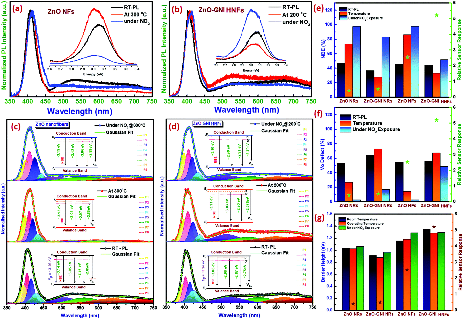 | ||
| Fig. 7 The operando PL spectra of (a) pristine ZnO nanofibers and (b) aligned ZnO-GNI nanofibers under ambient conditions, operating temperature and upon exposure to NO2. (c and d) Comparison of deconvoluted PL-NBE emission and DLs emission spectra. Bar chart showing area under the curve of (e) NBE emission, (f) DLs emission from the PL spectra (inset shows deep level energy diagram showing various defect states in the band gap of the materials) and (g) comparison of barrier height with relative sensor response for pristine ZnO and ZnO-GNI nanostructures under different conditions. | ||
Operando photoluminescence emission spectral studies were performed during electrical measurements to explore the defect-mediated NO2 sensing mechanism of ZnO-GNI heterojunction nanosystems through their unique features such as near band edge (NBE) emission and defect level emission behaviour during gas/material interactions. Scheme 1 shows the schematic illustration of experimental setup used for operando photoluminescence studies of porous ZnO-GNI nanosystems. Fig. 7 displays the emission spectra of pristine ZnO and ZnO-GNI nanofibers under different operating conditions. Similarly, the emission bands for ZnO nanorods and ZnO-GNI heterojunction nanorods are depicted in Fig. S7 (ESI†). The PL spectra were collected at room temperature and at operating temperature conditions in order to understand the influence of temperature on their structural and defect- mediated changes of the sensors in the absence of NO2 gas. Furthermore, PL spectra were acquired during NO2 exposure to study the role of defects in NO2 adsorption. The room temperature PL spectra of 1D pristine ZnO and ZnO-GNI nanorods and nanofibers in air was analysed by the presence of two major emission bands including a highly intense UV peak corresponding to the exciton luminescence and visible luminescence originated from the intrinsic defects existing in ZnO.51 The corresponding emission peaks of the observed complex band revealed that the intensity of edge luminescence is stronger than the intensity of visible luminescence, indicating the excellent crystalline quality of ZnO-GNI systems as depicted in Fig. 7 and Fig. S7 (ESI†).52
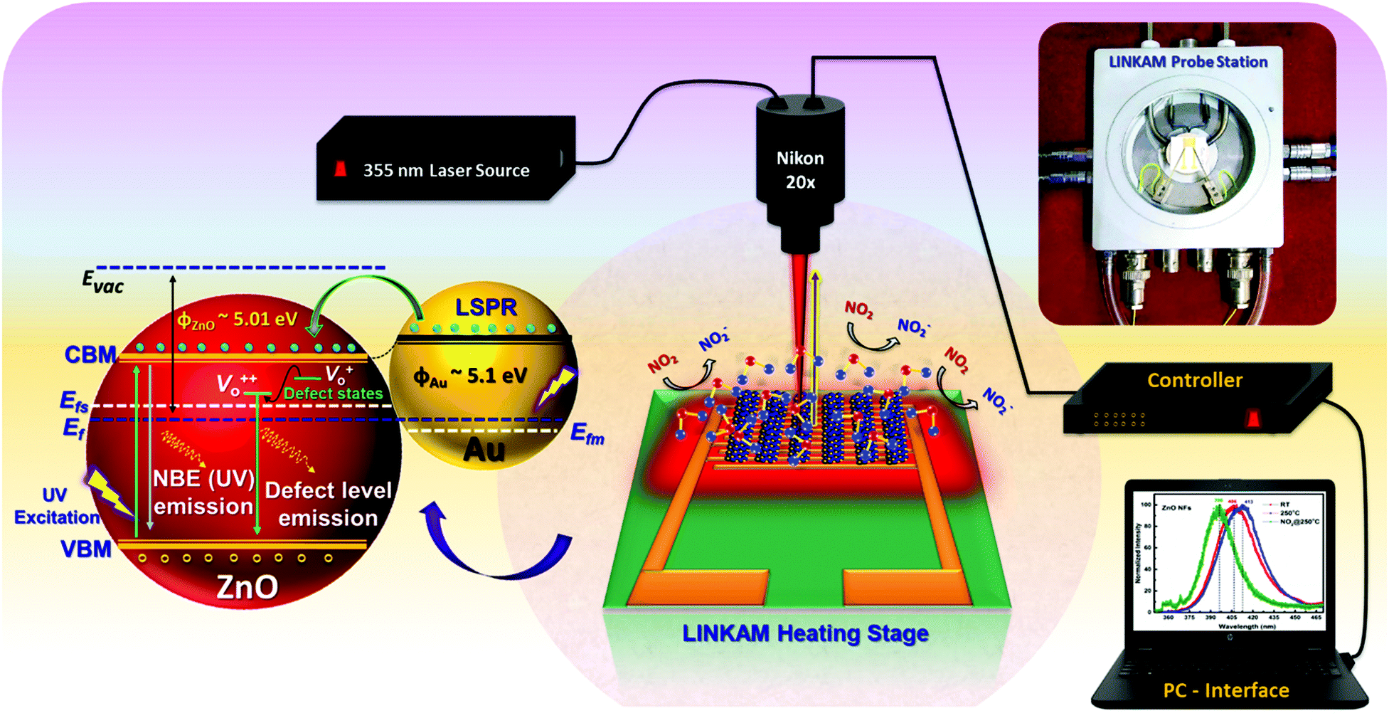 | ||
| Scheme 1 Schematic depiction of experimental set up used for operando photoluminescence studies performed for ZnO-GNI HNFs upon NO2 exposure. | ||
The room temperature PL emission spectra of all the investigated 1D materials are represented by the black line as shown in Fig. 7 and Fig. S7 (ESI†). Each material exhibited two major peaks, a near-band-edge (NBE) emission at ∼390 nm and deep levels (DLs) emission in the visible region of ∼490–750 nm. The dominant peak at the UV region is the NBE emission, which is due to the direct recombination of free-exciton including bound state excitons and shallow states. The DLs comprise of the major bands related to oxygen vacancies (V+o), oxygen interstitials (Oi), and zinc vacancies (VZn). The band at ∼500–540 nm originates from the non-radiative electron capture from the conduction band (CB) of ZnO by singly charged oxygen vacancy (V+o), leading to an unstable state that recombines with a photo-excited hole in the valence band (VB) of ZnO. However, the band between ∼550 and 610 nm corresponds to the grain boundary-induced depletion region which undergoes radiative recombination with the CB electrons. The peak within 610–750 nm is typically attributed to oxygen interstitials (Oi).53 A similar trend was observed in the emission spectra obtained under operational conditions (red line) and under NO2 exposure (blue line). It is clearly observed from the PL spectra depicted in Fig. 7(a and b) and Fig. S7(a and b) (ESI†) that, with increasing operating temperature, the NBE emission shows a red shift from 401 to 412 nm for ZnO nanorods, 400 to 404 nm for ZnO-GNI nanorods, 406–412 nm for ZnO nanofibers and 401–408 nm for ZnO-GNI nanofibers respectively. The band shifting of NBE emission is due to the increase in carrier density introduced by oxygen vacancies which indicates the narrowing of energy band gap evident from Table S4 (ESI†).54 The peak broadening and intensity variation were observed in the case of NO2 exposure, while the peak shifting was negligible since the concentration of NO2 was trace-level. Furthermore, in order to understand the relation between emission properties and gas sensing properties, the PL spectra were deconvoluted into Gaussian peaks and fitted with the experimental data. The deconvoluted NBE and DLs peaks of pristine 1D ZnO and ZnO-GNI nanosystems with corresponding energy level diagrams are shown in the Fig. 7(c and d) and Fig. S7(c and d) (ESI†). Initially, the relative area under the deconvoluted curves of NBE emission and DL emissions were estimated as shown in the bar chart in Fig. 7(e and f). The NBE emission clearly indicated a thermal quenching effect in the case of both ZnO-GNI nanorods and ZnO-GNI nanofibers under sensor operational conditions (red line). The results revealed that, due to the existence of Au nanoislands on the surface of core ZnO fibre, back spill-over phenomenon occurs i.e., excited electrons from ZnO can transfer back to Au producing more electron density at the Au centres of the ZnO-GNI heterojunctions.55 In the case of heterojunctions, electron transfer occurs due to the workfunction difference of the constituent materials, where, the metal (Au) work function (ϕm) is higher than that of the semiconductor (ϕs), i.e., ϕm > ϕs and hence the electrons flow from the CB of ZnO to Au. The electron transfer continues until the Fermi levels of Au and ZnO attain equilibration.56 Under the sensor operational conditions, Au nanoislands present on the surface of ZnO can extract more electrons from the conduction band of ZnO which further restrict the direct and trap related charge carrier excitons since the Fermi level (Ef) of Au nanoislands occurs beside the ECB of ZnO. Therefore, the thermal quenching of NBE emission was observed in the PL spectra of ZnO-GNI systems under the sensor operating temperature. The accumulation of charge density on Au induces more catalytic activity to make more ionosorbed oxygen species surrounding near to the Au/ZnO interfaces which leads to enhanced NO2 adsorption compared to pristine ZnO.
Furthermore, it is interesting to note that during NO2 exposure, the intensity of the NBE emission peak (blue line) of ZnO-GNI HNFs was increased compared to the NBE peak at working temperature, which means the self-trapped electrons; free electrons present in the CB of ZnO and electron rich Au centres have major roles in increasing the rate of NO2 adsorption on the surface of ZnO-GNI nanofibers and ZnO-GNI nanorods as inferred from Fig. 7(b and e). Whereas, the intensity of NBE emission of pristine ZnO nanofibers was found to be drastically reduced under NO2 exposure owing to the recombination dynamics as depicted in Fig. 7(a and e).20 Consequently, the enhanced sensitivity of ZnO-GNI nanofibers can be due to the 1D nanograined morphology having enormous active sites to adsorb more NO2 molecules than that of ZnO-GNI nanorods. Hence, the NO2 adsorption takes places mostly through spill-over by Au nanoislands significantly influenced by the charge recombination process during the gas/material interactions.
On the other hand, the DLs emissions consist of intrinsic defects such as oxygen vacancies (V+o, V++o), deep interstitials of oxygen (Oi), zinc (Zni) and anti-site oxygen (OZn) that may be formed on the surface of the pristine ZnO and ZnO-GNI nanostructures during the synthesis process, which may also have equal responsibility towards enhanced NO2 sensitivity.57,58 The broad DLs emission spectra were deconvoluted to evaluate the relative concentrations of structural defects present in pristine ZnO and ZnO-GNI nanosystems revealed in Fig. 7(c and d) and Fig. S7(c and d) (ESI†). Being under ambient conditions, the ZnO-GNI heterojunction nanosystems possessed more defect states compared to the pristine ZnO nanostructures as depicted in Fig. 7(e and f). During operational conditions, the intensity of DLs emission peaks decreases for pristine ZnO nanorods and nanofibers compared to that of ambient conditions, which could limit the rate of NO2 adsorption. Whereas, under operational conditions, the free excitons and self-trapped electrons were trapped by the Au nanoislands further becoming more negative and ZnO become more positively depleted, and shows enhanced DLs emission. Hence, the singly charged oxygen vacancies (V+o) and anti-site oxygen (OZn) play major roles in enhancing the NO2 sensitivity of ZnO-GNI nanofibers as evident from Fig. 7(c and d). During NO2 exposure, the DLs emission was found to be suppressed due to the adsorption of NO2 molecules on the surface of the materials. The relative concentration of V+o and OZn were quenched drastically as depicted in Table S5 (ESI†) compared to DLs emission observed under operational conditions owing to a charge recombination process occurring when NO2 molecules react with the dangling bonds present on the surface of the ZnO nanostructures as evident from Fig. 7(e and f). The oxygen vacancies (V+o) can bind more firmly with NO2 molecules drawing more electrons from ZnO surfaces compared to the defect-free ZnO surface and can also act as preferential adsorption sites for NO2 molecules.59 It is noteworthy that the enhanced sensitivity of ZnO-GNI nanofibers can be attributed to the nanograined structure having enormous active heterojunction sites to adsorb more NO2 molecules compared to the crystalline 1D ZnO-GNI nanorods.34 Based on the intricate analysis, we have understood that 1D aligned ZnO-GNI hetero-junction nanofibers possess enhanced sensing behavior due to the directed electron transport properties, hetero-junctions and formation of surface adsorbed oxide species, band-bending and spill-over sensitization, which have been justified by performing operando PL and electrical measurements. The NBE emission with deep level defects observed under operational conditions was found to be favoring the band bending process in the heterojunctions, which further aided in understanding the complex sensing mechanism in 1D aligned MOS heterojunction MOS nanofibers at reduced operating temperature.
Typically, ZnO-GNI nanofibers when exposed to an ambient environment under working temperature, surface adsorption of oxygen takes place resulting in seizure of free electrons and produces charge carrier separation on the surface of heterojunction nanofibers.60 Based on the value of β estimated from the transient NO2 sensor response plot, the ionosorbed oxide species on aligned ZnO-GNI HNFs are predominantly O− rather than O2− ions as illustrated in the graphic representation in Scheme 2(a and b). The energy band structure of pure ZnO and 1D aligned ZnO-GNI nanofibers were theoretically simulated using AFORS-HET v2.5 as depicted in Scheme 2. The constructed band diagram evidently depicted the upward bending state of the ZnO interface, while forming the ZnO-GNI heterojunctions as a result of their electron transfer due to the changes in position state of the Fermi level energy.61 The Fermi level of ZnO was found to align with that of Au when the electron transfer reaches equilibrium while forming the heterojunctions. The difference in CB and VB of ZnO and ZnO-GNI nanostructures were estimated from UV-DRS analysis as shown in Fig. S4 (ESI†) which was used as the input parameter for the simulation studies.
 | ||
| Scheme 2 Schematic illustration of band bending mechanism of ZnO-GNI HNFs under NO2 exposure. | ||
Upon NO2 exposure, Au nanoislands anchored over the ZnO nanofibers dissociate the adsorbed NO2 molecule into NO2− which further interact with the oxide ions existing near the interface resulting in the formation of NO2 as denoted in the relations below,62
| NO2(g) + e− → NO−2(ads-Au) | (3) |
| NO−2(ads)(Au) → 2O−2 + NO2 | (4) |
Due to the presence of surface ionosorbed oxide ions, the surface potential barrier drastically increased and thereby the resistance of the sensor increases which further leads to band bending at the ZnO interface. As evident from operando PL studies of ZnO-GNI nanostructures, the variation in the estimated percentage of area under the dominant band such as NBE emission and deep level defects (DLs) emission greatly influence the electrical properties and sensing performances. The inherent surface defects, (V+o, Zni and OZn) rigorously overwhelm the barrier height of Schottky ZnO-GNI which can turn into a conducting channel for free electrons in the aligned 1D heterojunction nanofibers. Moreover, as evident from the emission spectra, the unique SPR behaviour of Au nanoislands further confirmed the high-density e− carriers existing in the higher energy states that occur during e− transfer from ZnO to Au as depicted in Scheme 2. The effective back spill-over phenomenon aids in adsorption of more oxide species over the surface of ZnO-GNI HNFs.63 The operando studies based on PL and electrical measurements confirmed the development of barrier potential at the ZnO-GNI heterojunctions, which reduces the e− mobility and thereby broaden the trap depth (LD) compared to pristine ZnO leading to the band bending, one of the most pertinent phenomena that should be considered during gas sensor development. From the aforementioned experimental evidence, it can be understood that the influence of spill-over and back-spill effects on mechanism, plasmonic properties of Au nanoclusters, DLs defects and ideal band bending phenomenon enhance the rate of electronic sensitization process, apart from the directed electron transport due to the 1D structure of aligned ZnO-GNI HNFs. Table S7 (ESI†) compares the performance of ZnO-GNI nanofibers based NO2 sensors reported in the literature.35,39,43,64–67 It can be seen that the direct on-chip fabrication of 1D aligned ZnO-GNI nanofibers displays higher potential in detecting trace level concentration of NO2 gas compared to existing reports apart from the manufacturing feasibilities. The insights derived from the present investigation points towards the excellent potential of 1D aligned ZnO-GNI HNFs in detecting trace level NO2 gas at lower operating temperatures.
Overall, the effective strategy developed with this investigation for the single-step fabrication of 1D aligned ZnO-GNI HNFs directly onto the sensor device can be considered as a unique method for sensor development owing to its multiple benefits both in terms of ease of fabrication as well as superior sensor performance. The directed electron transport properties of the aligned multicrystalline ZnO-GNI HNFs not only acquired through an on-chip direct coaxial electrospinning with in situ photoreduction method, but also significantly promotes its NO2 sensing properties. Such aligned heterojunction nanofibers show superior sensing properties compared to its randomly oriented 1D nanorod structures. The outcome of this work suggests that on-chip fabrication of 1D aligned ZnO-GNI nanofibers could be a single-step and cost-effective fabrication process which opens up a new paradigm for the design and development of low-cost, aligned single nanofiber devices with improved selectivity for real time NO2 sensor applications and also bridge the gap between gas sensor research and industries for making better products.
4. Conclusions
To summarize, we have demonstrated an efficient direct on-chip fabrication of aligned ZnO-GNI HNFs based NO2 sensors using coaxial electrospinning with an in situ photoreduction method. The sensor fabrication method provides effective surface functionalization of nanofibers without any tedious and time-consuming steps. Aligned ZnO-GNI heterojunction nanofibers exhibited a higher sensor response (196%) with rapid response time towards 500 ppb trace level concentration of NO2. The superior sensor response was due to abundant active sites through nanograined morphology and presence of Au nanocatalyst sites that can seize more O− ions by spill-over effect on the ZnO surface leading to the development of larger potential barrier with more electron donors, along with the directed electron transport due to its 1D aligned structure. More insights towards the electronic sensitization mechanism of the ZnO-GNI HNFs were unveiled from operando PL and electrical studies, which endorsed the role of zinc interstitial defects and oxygen vacancy on the spill over process and charge transfer between ZnO and Au nanoislands. The study also unravelled the complex sensing mechanism associated with localised surface plasmon resonance while forming heterojunctions, which is responsible for the enhancement of NO2 sensing properties. The single-step production of aligned ZnO-GNI HNFs directly onto the sensor device can be considered as a promising strategy for developing high performance NO2 gas sensor devices for real-time applications.Conflicts of interest
There are no conflicts to declare.Acknowledgements
The authors acknowledge DST-SERB (Ref. No. SB/S3/CE/038/2015) for financial support. The authors also wish to acknowledge the facilities and support provided by the management, PSG Sons and Charities, Coimbatore. Authors thank Dr Anuradha Ashok and Dr T. Vijayaraghavan, PSG IAS, Coimbatore for TEM measurements and Mr Rajesh U. P., PSG IAS, Coimbatore for Operando PL measurements.References
- M. Wang, Y. Wu, N. Li, F. Zhao, Q. Zhao, J. Li and G. Liu, Chem. – Asian J., 2020, 15, 1484–1492 CrossRef CAS PubMed.
- A. Ziashahabi, M. Prato, Z. Dang, R. Poursalehi and N. Naseri, Sci. Rep., 2019, 9, 1–12 CAS.
- D. Wu, R. Jia, M. Wen, S. Zhong, Q. Wu, Y. Fu and S. Yu, Inorg. Chem., 2020, 59, 1218–1226 CrossRef CAS PubMed.
- Y. Zhao, G. Brocks, H. Genuit, R. Lavrijsen, M. A. Verheijen and A. Bieberle-Hütter, Adv. Energy Mater., 2019, 9, 1–11 Search PubMed.
- V. Ramakrishnan, K. G. Nair, J. Dhakshinamoorthy, K. R. Ravi and B. Pullithadathil, Phys. Chem. Chem. Phys., 2020, 22, 7524–7536 RSC.
- P. Chakrabarty, M. Banik, N. Gogurla, S. Santra, S. K. Ray and R. Mukherjee, ACS Omega, 2019, 4, 12071–12080 CrossRef CAS PubMed.
- T. Kashyap, S. Biswasi, A. R. Pal and B. Choudhury, ACS Sustainable Chem. Eng., 2019, 7, 19295–19302 CrossRef CAS.
- I. F. Article, 2020, 0–103.
- A. K. Elger and C. Hess, Sensors, 2019, 19(23) DOI:10.3390/s19235075.
- N. Sergent, M. Epifani, E. Comini, G. Faglia and T. Pagnier, Sens. Actuators, B, 2007, 126, 1–5 CrossRef CAS.
- J. Zhang, D. Zeng, Q. Zhu, J. Wu, Q. Huang and C. Xie, J. Phys. Chem. C, 2016, 120, 3936–3945 CrossRef CAS.
- P. Hozák, M. Vorokhta, I. Khalakhan, K. Jarkovská, J. Cibulková, P. Fitl, J. Vlček, J. Fara, D. Tomeček, M. Novotný, M. Vorokhta, J. Lančok, I. Matolínová and M. Vrňata, J. Phys. Chem. C, 2019, 123, 29739–29749 CrossRef.
- X. Xiao, L. Liu, J. Ma, Y. Ren, X. Cheng, Y. Zhu, D. Zhao, A. A. Elzatahry, A. Alghamdi and Y. Deng, ACS Appl. Mater. Interfaces, 2018, 10, 1871–1880 CrossRef CAS PubMed.
- D. Degler, N. Barz, U. Dettinger, H. Peisert, T. Chassé, U. Weimar and N. Barsan, Sens. Actuators, B, 2016, 224, 256–259 CrossRef CAS.
- C. Drouilly, J. M. Krafft, F. Averseng, S. Casale, D. Bazer-Bachi, C. Chizallet, V. Lecocq, H. Vezin, H. Lauron-Pernot and G. Costentin, J. Phys. Chem. C, 2012, 116, 21297–21307 CrossRef CAS.
- S. C. Navale, V. Ravi, D. Srinivas, I. S. Mulla, S. W. Gosavi and S. K. Kulkarni, Sens. Actuators, B, 2008, 130, 668–673 CrossRef CAS.
- K. Li, Y. Luo, B. Liu, L. Gao and G. Duan, J. Mater. Chem. A, 2019, 7, 5539–5551 RSC.
- N. Singh, V. Pandey, N. Singh, M. M. Malik and F. Z. Haque, J. Opt., 2017, 46, 199–203 CrossRef.
- B. Cho, M. G. Hahm, M. Choi, J. Yoon, A. R. Kim, Y. J. Lee, S. G. Park, J. D. Kwon, C. S. Kim, M. Song, Y. Jeong, K. S. Nam, S. Lee, T. J. Yoo, C. G. Kang, B. H. Lee, H. C. Ko, P. M. Ajayan and D. H. Kim, Sci. Rep., 2015, 5, 8052 CrossRef CAS PubMed.
- A. Cretì, D. Valerini, A. Taurino, F. Quaranta, M. Lomascolo and R. Rella, J. Appl. Phys., 2012, 111(7) DOI:10.1063/1.3700251.
- A. Bismuto, S. Lettieri, P. Maddalena, C. Baratto, E. Comini, G. Faglia, G. Sberveglieri and L. Zanotti, J. Opt. A: Pure Appl. Opt., 2006, 8(7) DOI:10.1088/1464-4258/8/7/S45.
- Y. Ma, T. W. Choi, S. H. Cheung, Y. Cheng, X. Xu, Y. M. Xie, H. W. Li, M. Li, H. Luo, W. Zhang, S. K. So, S. Chen and S. W. Tsang, Nanoscale, 2019, 11, 8736–8743 RSC.
- J. Z. Ou, W. Ge, B. Carey, T. Daeneke, A. Rotbart, W. Shan, Y. Wang, Z. Fu, A. F. Chrimes, W. Wlodarski, S. P. Russo, Y. X. Li and K. Kalantar-Zadeh, ACS Nano, 2015, 9, 10313–10323 CrossRef CAS PubMed.
- N. Van Hoang, C. M. Hung, N. D. Hoa, N. Van Duy and N. Van Hieu, J. Hazard. Mater., 2018, 360, 6–16 CrossRef CAS PubMed.
- H. Zhang, Y. Wang, X. Zhu, Y. Li and W. Cai, Sens. Actuators, B, 2019, 280, 192–200 CrossRef CAS.
- M. W. Ahn, K. S. Park, J. H. Heo, D. W. Kim, K. J. Choi and J. G. Park, Sens. Actuators, B, 2009, 138, 168–173 CrossRef CAS.
- X. Pan and X. Zhao, Sensors, 2015, 15, 8919–8930 CrossRef CAS PubMed.
- S. Steinhauer, E. Brunet, T. Maier, G. C. Mutinati and A. Köck, Conf. Nanotechnol., 2012, 1–4 Search PubMed.
- L. Yu, C. Li, S. Ma, Y. Li, L. Qi, M. Yin and X. Fan, Mater. Lett., 2019, 242, 71–74 CrossRef CAS.
- K. Smółka, A. Firych-Nowacka and M. Lefik, Open Phys., 2017, 15, 777–789 Search PubMed.
- D. H. Kang, N. K. Kim and H. W. Kang, Nanotechnology, 2019, 30(36) DOI:10.1088/1361-6528/ab2278.
- A. Nikfarjam, S. Hosseini and N. Salehifar, ACS Appl. Mater. Interfaces, 2017, 9, 15662–15671 CrossRef CAS PubMed.
- Y. Shiraishi, H. Tanaka, H. Sakamoto, N. Hayashi, Y. Kofuji, S. Ichikawa and T. Hirai, Langmuir, 2017, 33, 13797–13804 CrossRef CAS PubMed.
- D. V. Ponnuvelu, S. Abdulla and B. Pullithadathil, ChemistrySelect, 2018, 3, 7156–7163 CrossRef CAS.
- J. Wang, S. Fan, Y. Xia, C. Yang and S. Komarneni, J. Hazard. Mater., 2020, 381, 120919 CrossRef CAS PubMed.
- V. P. Dinesh, A. Sukhananazerin and P. Biji, J. Alloys Compd., 2017, 712, 811–821 CrossRef CAS.
- R. Udayabhaskar, B. Karthikeyan, P. Sreekanth and R. Philip, RSC Adv., 2015, 5, 13590–13597 RSC.
- S. J. Lee, H. J. Jung, R. Koutavarapu, S. H. Lee, M. Arumugam, J. H. Kim and M. Y. Choi, Appl. Surf. Sci., 2019, 496, 143665 CrossRef CAS.
- D. Veeran Ponnuvelu, S. Abdulla and B. Pullithadathil, Microporous Mesoporous Mater., 2018, 255, 156–165 CrossRef CAS.
- X. Li, G. Zhu, J. Dou, J. Yang, Y. Ge and J. Liu, Ionics, 2019, 25, 5527–5536 CrossRef CAS.
- S. Das, S. Mukhopadhyay, S. Chatterjee, P. S. Devi and G. Suresh Kumar, ACS Omega, 2018, 3, 7494–7507 CrossRef CAS PubMed.
- N. Joshi, L. F. da Silva, F. M. Shimizu, V. R. Mastelaro, J. C. M’Peko, L. Lin and O. N. Oliveira, Microchim. Acta, 2019, 186(7) DOI:10.1007/s00604-019-3532-4.
- N. Gogurla, A. K. Sinha, S. Santra, S. Manna and S. K. Ray, Sci. Rep., 2014, 4 DOI:10.1038/srep06483.
- R. Sankar Ganesh, M. Navaneethan, V. L. Patil, S. Ponnusamy, C. Muthamizhchelvan, S. Kawasaki, P. S. Patil and Y. Hayakawa, Sens. Actuators, B, 2018, 255, 672–683 CrossRef CAS.
- V. Ramakrishnan, K. K. Karuppanan, M. Aleem and B. Pullithadathil, Nanoscale Adv., 2020, 2, 4785–4797 RSC.
- D. V. Ponnuvelu, B. Pullithadathil, A. K. Prasad, S. Dhara, A. Ashok, K. Mohamed, A. K. Tyagi and B. Raj, Appl. Surf. Sci., 2015, 355, 726–735 CrossRef CAS.
- S. Choopun, A. Tubtimtae, T. Santhaveesuk, S. Nilphai, E. Wongrat and N. Hongsith, Appl. Surf. Sci., 2009, 256, 998–1002 CrossRef CAS.
- J. Dhakshinamoorthy and B. Pullithadathil, J. Phys. Chem. C, 2016, 120, 4087–4096 CrossRef CAS.
- M. Brötzmann, U. Vetter and H. Hofsäss, J. Appl. Phys., 2009, 106(6) DOI:10.1063/1.3212987.
- S. W. Choi, A. Katoch, J. H. Kim and S. S. Kim, ACS Appl. Mater. Interfaces, 2015, 7, 647–652 CrossRef CAS PubMed.
- J. H. Lin, R. A. Patil, R. S. Devan, Z. A. Liu, Y. P. Wang, C. H. Ho, Y. Liou and Y. R. Ma, Sci. Rep., 2014, 4, 1–8 Search PubMed.
- A. Galdámez-Martinez, G. Santana, F. Güell, P. R. Martínez-Alanis and A. Dutt, Nanomaterials, 2020, 10(5) DOI:10.3390/nano10050857.
- A. Senthamizhan, B. Balusamy, Z. Aytac and T. Uyar, CrystEngComm, 2016, 18, 6341–6351 RSC.
- S. P. Oberegger, O. A. H. Jones and M. J. S. Spencer, Comput. Mater. Sci., 2017, 132, 104–115 CrossRef CAS.
- Q. Zhu, J. Lu, Y. Wang, F. Qin, Z. Shi and C. Xu, Sci. Rep., 2016, 6, 1–9 CrossRef.
- W. Liu, D. Gu, J. W. Zhang, X. G. Li, M. N. Rumyantseva and A. M. Gaskov, Rare Met., 2020 DOI:10.1007/s12598-020-01564-5.
- X. Zhou, A. Wang, Y. Wang, L. Bian, Z. Yang, Y. Bian, Y. Gong, X. Wu, N. Han and Y. Chen, ACS Sens., 2018, 3, 2385–2393 CrossRef CAS PubMed.
- M. Bao, Y. Chen, F. Li, J. Ma, T. Lv, Y. Tang, L. Chen, Z. Xu and T. Wang, Nanoscale, 2014, 6, 4063–4066 RSC.
- G. Li, H. Zhang, L. Meng, Z. Sun, Z. Chen, X. Huang and Y. Qin, Sci. Bull., 2020, 65, 1650–1658 CrossRef CAS.
- Z. Yang, D. Zhang and H. Chen, Sens. Actuators, B, 2019, 300, 127037 CrossRef CAS.
- Z. Zhang and J. T. Yates, Chem. Rev., 2012, 112, 5520–5551 CrossRef CAS PubMed.
- D. Zhang, D. Wu, Y. Cao, X. Zong and Z. Yang, J. Mater. Sci.: Mater. Electron., 2018, 29, 19558–19566 CrossRef CAS.
- S. H. Hung and K. McKenna, J. Phys. Chem. C, 2019, 123, 21185–21194 CrossRef CAS PubMed.
- X. Chen, Y. Shen, X. Zhong, T. Li, S. Zhao, P. Zhou, C. Han, D. Wei and Y. Shen, J. Alloys Compd., 2019, 783, 503–512 CrossRef CAS.
- A. Gaiardo, B. Fabbri, A. Giberti, V. Guidi, P. Bellutti, C. Malagù, M. Valt, G. Pepponi, S. Gherardi, G. Zonta, A. Martucci, M. Sturaro and N. Landini, Sens. Actuators, B, 2016, 237, 1085–1094 CrossRef CAS.
- Y. Mun, S. Park, S. An, C. Lee and H. Woo, Ceram. Int., 2013, 1–8 Search PubMed.
- P. Rai, Y. S. Kim, H. M. Song, M. K. Song and Y. T. Yu, Sens. Actuators, B, 2012, 165, 133–142 CrossRef CAS.
Footnote |
| † Electronic supplementary information (ESI) available. See DOI: 10.1039/d1ma00094b |
| This journal is © The Royal Society of Chemistry 2021 |