
 Open Access Article
 This Open Access Article is licensed under a Creative Commons Attribution-Non Commercial 3.0 Unported Licence
Broadband SERS detection with disordered plasmonic hybrid aggregates†
Peng
Mao‡
ab,
Changxu
Liu‡
 *bc,
Qiang
Chen
*d,
Min
Han
d,
Stefan A.
Maier
*c and
Shuang
Zhang
*b
*bc,
Qiang
Chen
*d,
Min
Han
d,
Stefan A.
Maier
*c and
Shuang
Zhang
*b
aCollege of Electronic and Optical Engineering & College of Microelectronics, Nanjing University of Posts and Telecommunications, Nanjing 210023, P. R. China
bSchool of Physics and Astronomy, University of Birmingham, B15 2TT, UK. E-mail: s.zhang@bham.ac.uk
cChair in Hybrid Nanosystems, Nanoinstitut München, Fakultät für Physik, Ludwig Maximilians-Universität München, 80539 München, Germany. E-mail: Changxu.Liu@physik.uni-muenchen.de; Stefan.Maier@physik.uni-muenchen.de
dKey Laboratory of Intelligent Optical Sensing and Integration, College of Engineering and Applied Sciences, Nanjing University, Nanjing, 210093, P. R. China. E-mail: qiangchen@nju.edu.cn
First published on 14th October 2019
Abstract
Plasmonic nanostructures possessing broadband intense field enhancement over a large area are highly desirable for nanophotonic and plasmonic device applications. In this study, 3D Ag hybrid nanoaggregates (3D-Ag-HNAs) are achieved via a highly efficient oblique angle gas-phase cluster beam deposition method. Not only can such structures produce a high density of plasmonic hot-spots to improve Raman sensitivity, but more importantly they generate kissing point-geometric singularities with a broadband optical response. We succeed in obtaining an experimental SERS enhancement factor beyond 4 × 10⁷ in the visible range, providing an optimal sensing platform for different analytes. Combined with good uniformity, reproducibility and ease of fabrication, our 3D-Ag-HNA offers a candidate for new generations of SERS systems.
Introduction
Enhancing the optical response of a plasmonic nanomaterial under incident light is essential to improving the performance in nanophotonic and plasmonic device applications, such as energy-harvesting devices,1 metamaterials,2–4 photocatalysis5 and surface-enhanced Raman spectroscopy (SERS).6–9 Among them, SERS is an extensively studied analytical tool that provides molecule-specific information on the molecular structure and chemical composition of analytes through Raman scattering. It is now generally accepted that the SERS enhancement arises from the enlarged local electromagnetic (EM) fields near a nanostructured metal system, which is resulted from localized surface plasmon resonances (LPRs),10 known as plasmonic “hot-spots” that occur near sharp asperities and in nanometer gaps between metal nanostructures such as nanoparticles (NPs),11,12 NP-spacer-film systems,13,14etc. Generally, the number and intensity of plasmonic hot-spots largely determines the SERS capability of a given substrate.15Hot-spots are manipulated by the size of NPs, the period of NP arrays, the shape of NPs, or the size of a nanoscale gap between two NPs.16,17 Generally, there are two ways to fabricate SERS substrates with well-defined hot-spots, the so-called top-down method and the bottom-up method. The bottom-up approach is usually based on the self-assembly process by using molecular ligands.18 However, most of the reported SERS hot-spots exist in two-dimensional (2D) planar geometries, limiting the maximum number of hot-spots to a single Cartesian plane.19–21 To address this issue, 3D plasmonic nanostructures with extension in the third dimension are actively pursued by increasing the number and utility of hot-spots in all three dimensions. Recently, several strategies have been proposed to construct 3D SERS substrates, such as reactive ion etching,22 template metal deposition,23 electron beam lithography24 and direct chemical growth.25 While most of the work emphasizes the enhancement factor of SERS systems at a single wavelength, the whole process of Raman scattering is substantially sensitive to the optical frequency.26 From the point of view of optics, the light–matter interactions strongly vary with wavelength; e.g., cyanine (Cy7)27 has the absorption peak in the near-infrared while rhodamine 6G in the visible. Despite lacking a proportional relationship between absorption and Raman intensity,26 the wavelength of the laser can be properly optimized for the maximum number of scattered photons, i.e., SERS signal. While lasers at different frequencies are readily available, a SERS substrate with a broadband enhancement factor is of substantial importance considering the multifunctional usage. However, research on SERS with broadband features steps quite behind the efforts to boost the enhancement factor at a single wavelength.7,28 Most SERS substrates can only be used for an individual excitation wavelength, since the working band of these plasmonic nanostructures is always narrow. Therefore, different substrates have to be designed and fabricated to fit various excitation sources and analytes, which consumes more bio/chemical materials, substrates and measurement time.
Inspired by the recent advancements in transformation optics (TrO),29,30 here we propose and realize a broadband SERS substrate composed of 3D Ag hybrid nanoaggregates (3D-Ag-HNAs). Kissing points between the nanoclusters readily produce geometric singularities, which introduce a broadband optical response across the full visible wavelength according to TrO.1,31,32 Meanwhile, 3D-Ag-HNAs that contain dense plasmonic hot-spots with strong field enhancements over a large area guarantee cascaded optical field enhancement (CFE) and consequently high SERS sensitivity. After full-wave FDTD simulations, we experimentally demonstrate a SERS substrate with the enhancement factor beyond 4 × 10⁷ from 473 nm to 633 nm in the visible. Besides, the gas-phase cluster beam deposition approach33 used here provides a high quality of uniformity and reproducibility, shedding light on a new paradigm for SERS substrates.
Experimental section
Fabrication of 3D-Ag-HNA
One 3D columnar Ag HNA was composed of large-size Ag NPs and small Ag cluster aggregates, as shown in Fig. 1. The larger Ag NPs were prepared in a self-assembly manner by solid-state dewetting of thin metal films (deposition of an Ag film followed by annealing)34 (Fig. 1(a)). Ag films were deposited on bare silica glass substrates by thermal evaporation with film thicknesses of 8 nm. The deposition was carried out with a home built multifunctional coating system with a working pressure of 1.0 × 10⁻⁴ Pa and a deposition rate of 0.5 nm s−1. The deposition rate was monitored by using a quartz crystal microbalance. During the deposition, the evaporation flux can be cut off by a shutter instantly to allow careful control of the deposition mass. The post-deposition annealing process was performed for 15 min in situ with a temperature of 350 °C.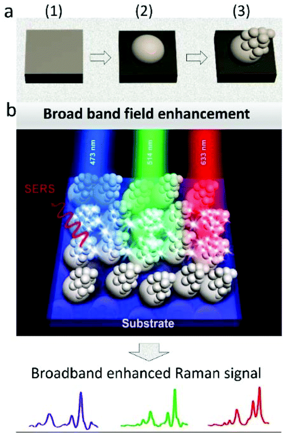 | ||
| Fig. 1 (a) Schematic illustration of the fabrication process for 3D Ag hybrid nanostructures: (1) deposition of Ag thin films; (2) solid state dewetting process; (3) oblique cluster beam deposition. (b) Cartoon of the 3D-AgHNA structure for broadband SERS detection. | ||
An oblique angle cluster beam deposition process was used to deposit smaller Ag cluster layers on a substrate surface with large Ag NPs. In our fabrication, Ag clusters were generated in a magnetron plasma gas aggregation cluster source and deposited on substrates obliquely,35 as shown in Fig. 1(a). The deposition was performed in a high-vacuum chamber equipped with the cluster source, as shown in Fig. 2(a). An Ag target with high purity (99.99%) was used as the sputtering target. The magnetron discharge was operated in an argon stream at a pressure of about 120 Pa in a liquid nitrogen-cooled aggregation tube. Ag atoms were sputtered from the target and Ag clusters were formed through the aggregation process in the argon gas. The clusters were swept by the gas stream into high vacuum through a nozzle, forming a collimated cluster beam with a high speed of ∼1000 m s−1 (more details in the ESI†). The substrate was tilted so that the incident cluster beam direction made a 60° angle against the normal of the substrate surface. The deposition was carried out at a rate of 0.5 ± 0.1 Å s−1 for 15 min.
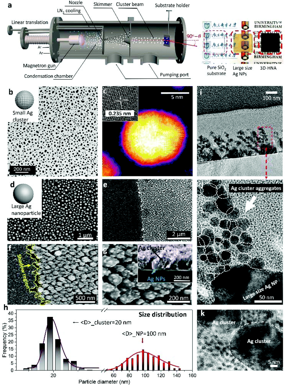 | ||
| Fig. 2 (a) Left: Schematic illustration of the gas phase cluster beam deposition system. Right: Photographs of the blank SiO2 substrate, large size Ag NP sample and 3D-HNA sample. (b) TEM image of Ag clusters generated from the cluster deposition system. (c) Typical HAADF-STEM image of a single Ag cluster. The inset is the HR-STEM image of the Ag cluster and the corresponding lattice constant has been marked in the figure. (d) SEM image of large size Ag NPs from the solid-state film dewetting process. (e) A typical SEM image of Ag cluster assembles (left part) and 3D-Ag-HNA (right part). (f) A high magnification SEM image of Ag cluster assembles (left part) and 3D-Ag-HNA (right part), the shadowing region has been marked in the figure. The inset shows a typical cross-sectional SEM image of 3D-Ag-HNA. (g) A high magnification SEM image of 3D-Ag-HNA. The inset shows a high magnification cross-sectional SEM image of 3D-Ag-HNA. (h) Size distribution of the Ag nanoparticles in the 3D-Ag-HNA and the corresponding log-normal fits. (i) TEM image of 3D-Ag-HNA. (j) A high magnification cross-sectional TEM image of a single unit in the 3D-Ag-HNA structure. (k) A high magnification TEM image of two Ag nanoclusters in the aggregate. | ||
Structure and characterization
The structural morphology of small Ag clusters was characterized by using scanning transmission electron microscopy (STEM). The STEM investigation was performed using a JEOL instrument (JEM2100F) with a spherical-aberration corrector (CEOS GmbH). The images were acquired using high-angle annular dark field (HAADF) and bright field (BF) detectors. The structural properties of 3D-Ag-HNA were characterized by scanning electron microscopy (SEM, HITACHI S4500).Optical measurements and FDTD simulation
The extinction spectra of 3D plasmonic nanostructures were recorded using a UV-Vis spectrophotometer (Omni-λ300, Zolix Co. Ltd) equipped with a Hamamatsu CR2658 photomultiplier-tube and a deuterium lamp/halogen tungsten lamp combined light-source. FDTD calculations utilizing a commercial software (FDTD Solutions, Lumerical Inc.) are used to simulate the electromagnetic field distribution of the 2D nanoparticle and 3D-Ag-HNA. The optical constants of silver are taken from Johnson and Christy. The 3D-Ag-HNA plasmonic nanostructures were simplified in the simulations by assuming that the bottom Ag nanostructures formed spheres of 100 nm in diameter. Top columnar Ag cluster aggregates were located on the top of randomly distributed large size Ag NPs. All the small Ag clusters were modelled as spherical in shape. A linearly polarized plane wave illumination beam was directed onto the 3D plasmonic nanostructure.SERS measurements
To assess the SERS ability of the 3D-Ag-HNA substrates, a typical organic analyte rhodamine 6G (R6G) was used as a probe molecule. To prepare the samples for R6G detection, the 3D-Ag-HNAs were immersed in the R6G-ethanol solution for 15 min and then the SERS substrates were rinsed with pure ethanol several times. Lastly, the SERS substrates were dried under N2 flow. Raman spectra are recorded on an upright-configured confocal microscope (NT-MDA NTEGRA SPECTRA) equipped with a 100× objective lens. To obtain the broadband SERS signal, three lasers with wavelengths of 473 nm, 514 nm and 633 nm were used separately as excitation sources. Raman mappings are performed in a sample-scanning mode with a step of 0.5 μm per point and a dwell time of 1 second per point.Results and discussion
The structural characterization of a typical Ag cluster array generated from the cluster source is shown in the STEM images in Fig. 2(b). As seen, the shape of the Ag cluster is approximately spherical. The size of Ag clusters generated from the gas-phase cluster beam deposition system is not absolutely uniform, with a log-normal distribution for the size statistics. Fig. 2(c) shows the HAADF-STEM and BF-STEM images of a single Ag cluster. The lattice fringes have an inter-planar spacing of 0.235 nm, corresponding to the (111) planes of the face-centered cubic (FCC) structure of metallic Ag. Such a crystalline nature of the Ag clusters improves the plasmonic enhancement and the stability of the system.36–383D Ag HNAs were prepared by performing oblique angle cluster beam deposition on a substrate with large Ag NPs. In such a process, the large-size Ag NPs produced shadow regions unreachable for the incident Ag cluster flux, as shown in the ESI (Fig. S1†). In the non-shadow areas (top of the Ag NPs) the incident cluster flux can deposit preferentially. As a result, the Ag clusters piled up and formed a columnar 3D hierarchical nanostructure. Fig. 2(d) shows a typical SEM image of large size Ag NPs from the solid film dewetting process. The average size of the Ag NPs is 100 nm and the Ag nanoparticles are randomly distributed on the substrate surface. Without large Ag NPs acting as obstacles on the substrate, only a porous Ag cluster layer forms on the substrate surface, as shown in Fig. 2(e and f). Fig. 2(g) shows a high magnification SEM image of the deposited 3D-Ag-HNA structure. The formation of extreme porous and columnar cluster piling is a result of the shadowing effect as mentioned.
This structure provides a new paradigm to realize 3D SERS substrates with high particle density. The high-magnification SEM image presented as an insert in Fig. 2(g) shows that the 3D Ag nanostructure comprised 3D-stacked hybrid assemblies. In each of the assemblies, a larger Ag NP (∼100 nm) was decorated with smaller Ag cluster (∼20 nm) aggregates. In gas-phase cluster beam deposition, all the nanoclusters are formed before arriving at the substrate, guaranteeing good touching points for geometric singularities.35 A statistical analysis on the Ag NPs in SEM images demonstrated bimodal size distribution, as shown in Fig. 2(h). To further investigate the structural properties of 3D-Ag-HNA, cross-sectional TEM images were taken from the sample slice, as shown in Fig. 2(i–k). Fig. 2(i) shows a typical TEM image of 3D-Ag-HNA, and tilted columnar cluster piling could be unambiguously observed. The high magnification TEM image further demonstrated that highly porous Ag clusters piling with nanoscale internal gaps formed in the 3D-Ag-HNA, as shown in Fig. 2(j). The “kissing” configuration of two clusters in the aggregates could also be observed, as shown in Fig. 2(k).
The local EM field enhancement due to hot-spot generation provides the primary mechanism underlying signal amplification in SERS. For the clarification of the broadband response and the enhanced plasmonic coupling in 3D-Ag HNA, 3D numerical calculations were carried out by using the finite-difference-time-domain (FDTD) method.39 A linearly polarized plane wave illumination beam with wavelengths of 473 nm, 514 nm and 633 nm, corresponding to the Raman excitation wavelength in SERS investigation, was directed onto the plasmonic nanostructures. Based on the SEM images, each of the hybrid aggregates was modeled as one 100 nm Ag NP decorated with 20 nm Ag clusters on top. This model could reasonably provide information on the plasmonic couplings not only between the smaller Ag clusters but also between smaller Ag clusters and larger Ag NPs.
A comparison of the electric field distributions across 3D-Ag-HNA and large size Ag NPs is shown in Fig. 3(a) and (b). Fig. 3(a) shows the electric near-field intensity profile around the Ag HNA at three representative wavelengths, i.e., 473, 514, and 633 nm, respectively. The electric field was highly concentrated around the “kissing points” not only between neighboring small Ag clusters but also between adjacent Ag small clusters and Ag large NPs, for all of the three excitation wavelengths, as a result of adiabatic focusing.31,32 These “kissing” configurations could trigger a process of broadband absorption, as it was reported in previous studies by performing TrO methods.1,29–32 A theoretical analysis can be found in the following section.
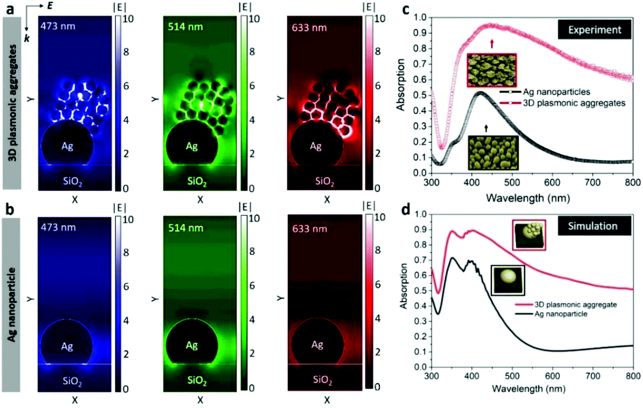 | ||
| Fig. 3 Simulated electric field distribution of 3D Ag HNA (a) and conventional Ag NPs (b) under different excitation wavelengths (473 nm, 514 nm and 633 nm). Experimental (c) and simulated (d) optical absorption of the large size Ag NPs and the 3D-HNAs. | ||
Meanwhile, for 3D-Ag-HNA, field enhancements were generated through the three near-field coupling effects associated with coupling (1) between top smaller Ag clusters and the underlying larger Ag NPs, (2) between the smaller Ag clusters themselves on the bottom Ag NPs, and (3) between Ag cluster aggregates decorated with two different adjacent structures. Firstly, the plasmonic coupling between top Ag clusters and the underlying larger Ag NPs could greatly concentrate and elevate the electric field, leading to cascaded optical field enhancement. Secondly, these clusters form an aggregate in 3D, which can support much more hot-spots than the 2D case. Ideally, the total number of hot-spots in a well-assembled 2D array is three times the number of particles. It has been investigated that 3D nanostructures can generate much more than one third the number of hot-spots of the 2D nanostructure.19 Thirdly, plasmonic coupling between the two different adjacent columnar structures will create an extremely high electric field enhancement due to the cavity resonances, which resembles the coupling mode in the Ag nanorod array.40
The average SERS signal intensity is approximately proportional to the fourth power of the local electric field enhancement (i.e., |E|4/|E0|4, where |E0| and |E| are the incident and local electric field intensity).41 In many cases, this approximation is a good indicator of the order of magnitude of the SERS enhancement factor (EF). Most importantly, we modeled the hot-spot distributions of the 3D-Ag-HNA at different incident wavelengths (473 nm, 514 nm and 633 nm). Hot-spots can occur at all simulated wavelengths in the 3D-Ag-HNA, while the field enhancement is fairly weak in the conventional 2D structure, especially at the wavelength positions (514 nm and 633 nm) which is far away from the resonance peak wavelength, as shown in Fig. 3(b).
To further study the optical properties of the 3D-Ag-HNA, we measured and simulated the far-field absorption spectra of the 2D and 3D structures. Fig. 3(c) presents an experimental comparison between the 3D-Ag-HNA and the conventional 2D nanostructure without top clusters. The black line is the absorption spectra of large-size Ag NPs, which shows a strong LSP resonance peak at 450 nm. The 3D-Ag-HNA showed a remarkably enhanced light absorption across a broad spectrum range from 400 nm to 800 nm, implying broadband strong plasmonic resonances in the 3D nanostructure.
Fig. 3(d) presents the simulated optical absorption of the 3D-Ag-HNA and the conventional 2D NPs. As seen in the figure, the plasmonic resonance of the 3D-Ag-HNA was much stronger and broader than the 2D Ag NPs. Interestingly, these simulated results agreed well with the measured optical absorption properties of the 3D and 2D plasmonic structures. The discrepancy in the resonance peak positions between the calculated and the measured spectra might be ascribed to the difference between the real nanostructure and the simplified model, such as the size distribution of Ag clusters, the actual location of the smaller Ag clusters relative to the larger Ag NPs, etc.
We further apply 3D-Ag-HNAs as broadband-SERS substrates for ultrasensitive molecule detection with excitations of 473, 514 and 633 nm. To assess the SERS ability of the 3D-Ag-HNA substrates, we investigate the sensing capability of the as-prepared 3D-Ag-HNA in detecting a typical organic analyte Rhodamine 6G (R6G) as a probe molecule using a SERS technique. Fig. 4(a) shows a typical SERS spectrum from the R6G treated 3D-Ag-HNA substrate. The positions of the characteristic peaks of R6G including 613, 775, 1187, 1309, 1360, 1506, 1569 and 1648 cm−1 could be clearly found in the spectrum, which are in agreement with previous studies.7,42
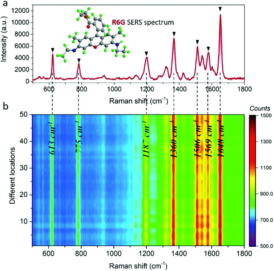 | ||
| Fig. 4 (a) Average SERS spectra measured from the R6G-treated 3D Ag hybrid nanostructure under the excitation laser wavelength of 473 nm. The concentration of R6G used in the measurement is 10−7 M. (b) SERS contour plot of R6G (10−7 M) on the R6G-treated 3D-Ag-HNA substrate at 50 different locations. | ||
The homogeneity of Raman signals is vital to SERS based sensors for a quantitative determination of target analytes. To evaluate the homogeneity of the Raman signal on the 3D hybrid structure, we detect the SERS spectra of R6G molecules with a concentration of 10−7 M at 50 randomly selected locations within an area of 30 × 30 μm, as shown in Fig. 4(b). All 50 locations display an impressive capability to enhance the intensity of R6G Raman signals without significant peak shifts.
To demonstrate the broadband sensing performance, we employed three laser lines at 473 nm, 514 nm and 633 nm to excite the 3D-Ag-HNA SERS substrate. Fig. 5(a)–(c) compares the Raman spectra between the 3D-Ag-HNA substrate and the Ag NP substrate at different excitation wavelengths. The 3D-Ag-HNA exhibited superior SERS performance compared to the 2D Ag NP nanostructure, with signal intensity 45.4 better. SERS signals can be observed with clear peaks at all excitation wavelengths (473 nm, 514 nm and 633 nm). The Raman intensity at 1360 cm−1 on the substrates, which is assigned to the aromatic C–C stretching of the R6G molecule,43 is selected for enhancement factor (EF) estimation. We estimate the sensitivity by using the SERS enhancement factor (EF), which is defined by comparing the intensity of the SERS signal with that of the non-SERS signal:10,42
| EF = (ISERS/CSERS)/(Iref/Cref) | (1) |
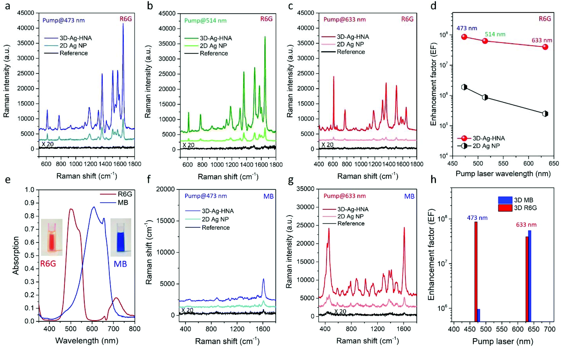 | ||
| Fig. 5 SERS spectra measured from the R6G-treated 3D Ag HNA, conventional 2D Ag NPs and smooth Ag film (reference), the excitation laser wavelength is (a) 473 nm, (b) 514 nm and (c) 633 nm, respectively. (d) Enhancement factor of the 3D Ag hybrid nanostructure under different laser wavelengths. The laser power used on the 3D-Ag-HNA substrate was 100 μW, while on the 2D Ag NP substrate and the reference substrate the laser power was 1 mW. (e) Optical absorption of R6G and MB. SERS spectra measured from the MB-treated 3D Ag HNA, conventional 2D Ag NPs and smooth Ag film (reference), the excitation laser wavelength is (f) 473 nm and (g) 633 nm, respectively. (h) Calculated EF of R6G and MB on the 3D-Ag-HNA SERS substrate under different laser wavelengths. | ||
For practical usage, a SERS substrate with detectability for different analytes is desirable. The intensity of a Raman scattering process varies strongly with the laser wavelength for a specific chemical. Consequently, a broadband SERS system can provide the flexibility to tune the laser frequency for optimization. To demonstrate this concept, we add a second dye, methylene blue (MB). Fig. 5(e) shows the optical absorption spectra of R6G and MB, demonstrating the difference in optical response presented by analytes. SERS measurements were implemented under excitation wavelengths of 473 nm and 633 nm, as shown in Fig. 5(f and g). SERS EFs of 6.6 × 10⁶ and 2.2 × 10⁷ are also calculated for the 3D-Ag-HNA substrate upon excitation at 473 nm and 633 nm. Fig. 5(h) provides a brief guide for sensing such two types of dyes from the value of EF at different wavelengths. The sensitivity of R6G is better with a 473 nm laser, while MB detection can be improved by using a laser at 633 nm. Considering the broadband enhancement in the 3D-Ag-HNA system, it offers excellent potential for a repertoire of analytes interacting with photons in the visible spectrum.
The detection limit for R6G is one of the most important parameters for evaluating the SERS sensitivity of a substrate.44 To evaluate the detection limit of our substrate, we implemented a SERS measurement with different R6G concentrations from 1 × 10⁻⁵ to 1 × 10⁻¹² M, as shown in Fig. 6(a). The SERS intensity decreases when reducing the concentration of R6G, but with distinguishable peaks, even at the low concentration of 10−12 M. The detection limit may be further lowered by other means, such as increasing the integration time. The Raman peaks at 613 cm−1 and 1360 cm−1 were selected for the quantitative analysis of R6G. The dependence of their intensities on R6G concentration is shown in Fig. 6(b). The error bars indicate the standard deviation of the peak intensities over different positions. The log–log plot of Raman intensity at 613 cm−1 and 1360 cm−1versus concentration shows a linear relationship, as seen in Fig. 6(b). Small correlative efficiency (R2 = 0.98888 for 613 cm−1 and R2 = 0.98958 for 1360 cm−1) suggests the potential for quantitative SERS analysis.45
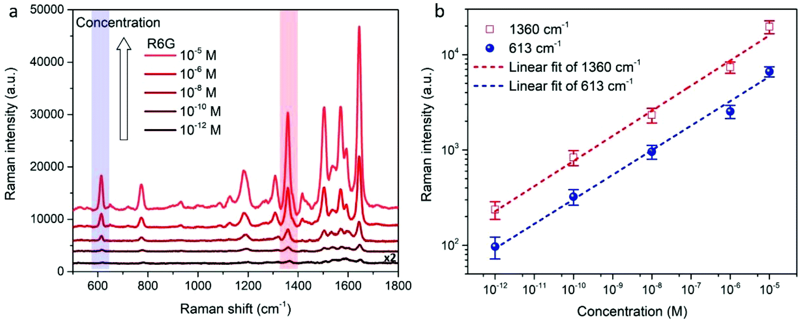 | ||
| Fig. 6 (a) The Raman spectra of R6G with different concentrations adhered on the 3D-Ag-HNA SERS substrate, and in order to be clarified, the spectrum of 10−12 M R6G was multiplied by 2 fold. (b) The SERS intensity of R6G peaks at 613 cm−1 and 1360 cm−1 on 3D-Ag HNA as a function of the molecular concentration, on a log scale. | ||
SERS is an essential analytical method that can be used to obtain fingerprint information of a target molecule. The uniformity and reproducibility of the active substrate are crucial for using SERS in real-life applications.46 To investigate the reproducibility, we first measured the substrate-to-substrate SERS signal from different batches, as illustrated in Fig. 7(a). The relative standard deviation (RSD) is used to represent performance stability with 20% as an acceptable threshold for practical applications.47,48 Here, we achieved a RSD value of 16.54% at 1360 cm−1 from six substrates of different batches, confirming good substrate-to-substrate reproducibility. To further investigate the uniformity and reproducibility of a single substrate, Raman mappings with different excitation lasers were performed in sample-scanning mode with a step of 0.5 μm per point and a dwell time of 1 s per point. Fig. 7(b–d) illustrate the measured rectangular region with the brightness of the grid being proportional to the signal intensity at 1360 cm−1. A statistical analysis was conducted based on the extracted 1360 cm−1 peak intensities, as shown in Fig. 7(e–g). The RSD is well controlled below 10% (8.32%@473 nm, 7.55%@514 nm and 9.26%@633 nm, more information in the ESI†), by virtue of the highly uniform substrates. In spite of the better RSD values reported by using top-down nanofabrication methods,46,49 the proposed 3D-Ag-HNA SERS substrate shares the advantages including the large-area fabrication with low cost and high EF value in a broadband.
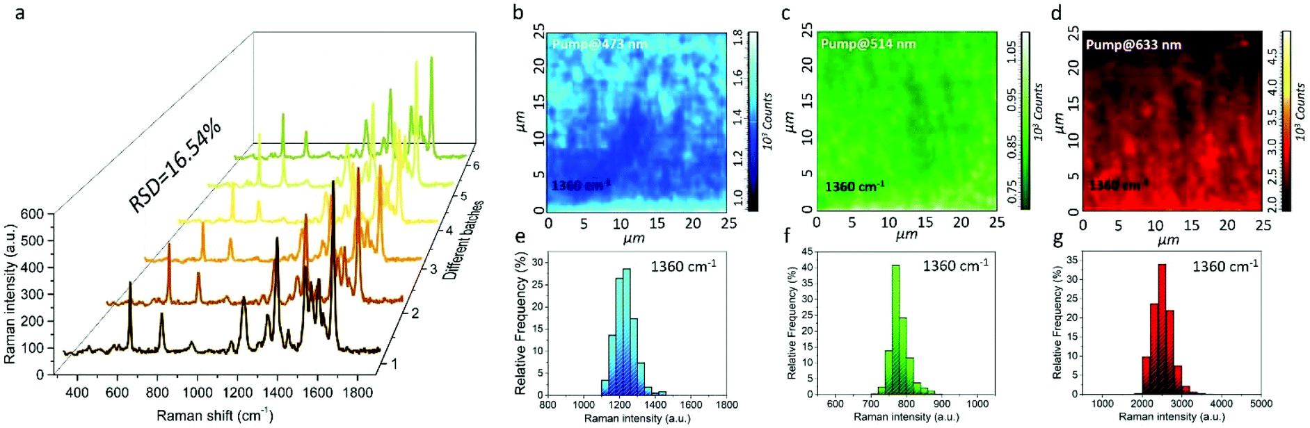 | ||
| Fig. 7 (a) SERS spectra of 10−7 M R6G collected from six 3D-Ag-HNA substrates of different batches. Raman intensity spatial distribution of the R6G 1360 cm−1 band over the mapping area obtained at the excitation wavelength of (b) 473 nm, (c) 514 nm and (d) 633 nm. Histograms of Raman intensities at 1360 cm−1 under different laser excitations: (e) 473 nm, (f) 514 nm and (g) 633 nm. | ||
Theoretical analysis
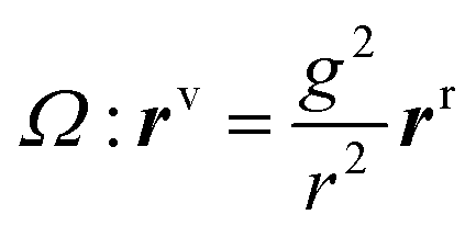
Here we provide an analytical model for our 3D-Ag-HNA structures with kissing points, explaining the broadband enhancement theoretically. For the simplicity but without loss of generality, we select the key part of our structure – two kissing silver nanoclusters with a point contact, which is demonstrated in Fig. 8a. The radius of the nanoparticle is R1 and R2 respectively and the polarisation of the light is along the x axis. Based on the idea of TrO, we can apply a coordinate mapping Ω:50where rr and rv are the coordinates in the real and virtual space, r is the distance to the origin and g is the scale factor. After mapping, the twin nanoparticle with a kissing point in real space is transformed to a configuration composed of two infinite plates with a distance of d = g2/2R1 + g2/2R2, as illustrated in Fig. 8b. To guarantee the invariance of the Maxwell equation under the transformation, the permittivity in the virtue space should be modified as follows:50
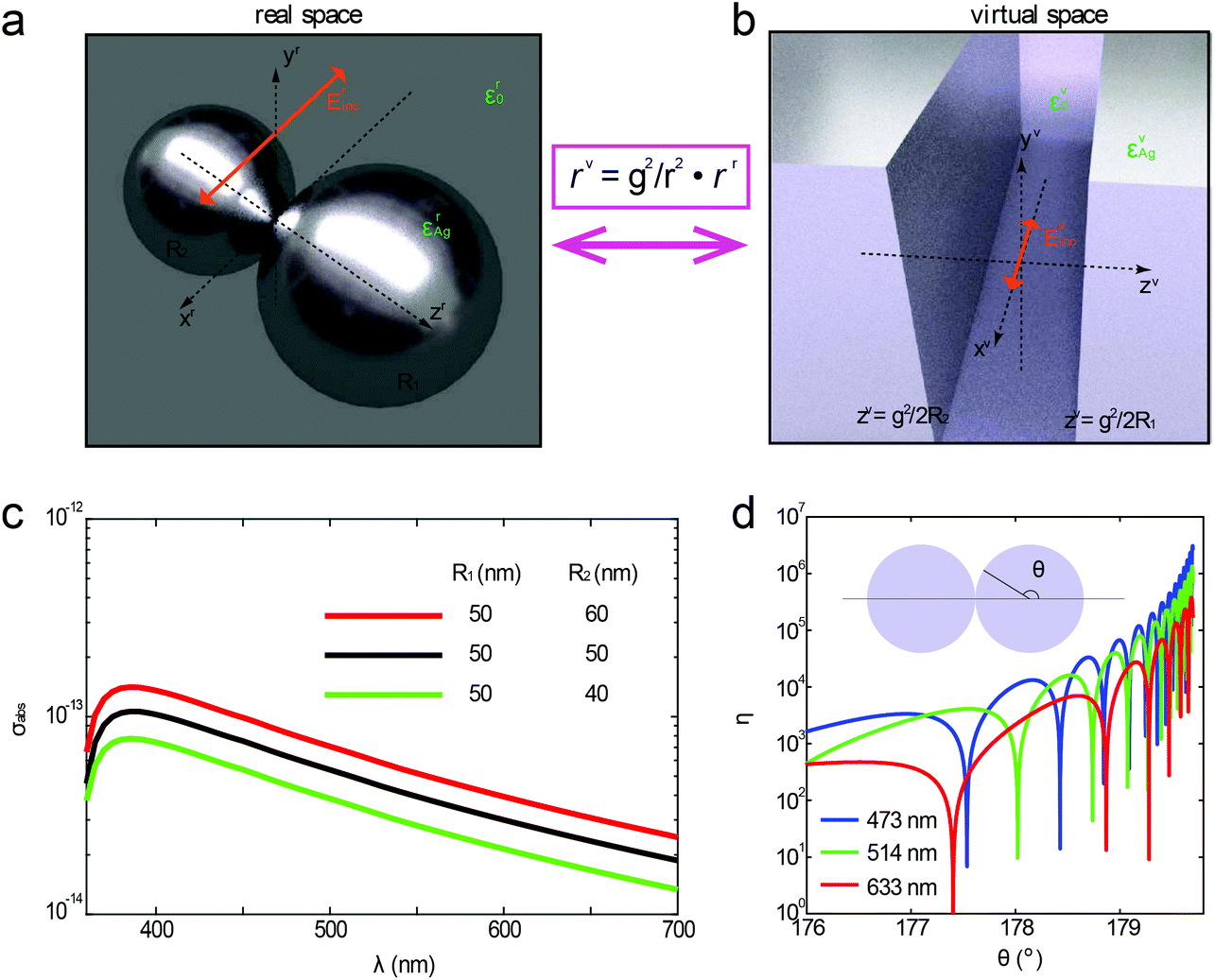 | ||
| Fig. 8 Theoretical analysis for the broadband enhancement of the nanoparticles with kissing points. (a) Schematic of a pair of nanoparticles with a point contact in real space. (b) The metal–insulator–metal structure can be achieved by coordinate transformation from real to virtual space. (c) The absorption cross-section σabs with different values of R1 and R2. (d) The field enhancement η at three different wavelengths used in SERS measurement. | ||
In the transformed virtual space, surface plasmon polaritons (SPPs) can be excited in a broad spectrum. In addition, the SSPs transmitting from the origin to infinity can be mapped back to the region around the kissing point, securing the gigantic field enhancement at that areas. Therefore, the MIM structure in the virtual space provides a more straightforward picture demonstrating the advantage of using kissing nanoparticles as a SERS substrate.
By using the quasi-static approximation51 and surface charge corrections,52 the electrodynamics can be solved analytically in the virtual space and transformed back to real space. The absorption cross section can be approximated to:49

We calculate σabs with different radii as demonstrated in Fig. 8c. The value of R1 and R2 is selected from the statistics in Fig. 2h. While the absorption cross section varies with different values of R1 and R2, the broadband response always holds.
Besides, the field enhancement near the kissing point can be derived as follows:52

Here we calculate the enhancement at three different wavelengths matching our SERS experiments, as demonstrated in Fig. 7d. Here we choose R1 = R2 = 50 nm. Owing to the broadband field enhancement explained above, we observe that the electric field is dramatically intensified at the kissing point at all three wavelengths, which is desired for the broadband SERS detection with good accuracy.
Conclusion
In conclusion, we designed and fabricated a novel 3D-Ag-HNA by a gas-phase cluster beam deposition approach, which can support dense hot-spots with high electric field enhancements over a large area. The 3D-Ag-HNA shows a broadband plasmonic resonance in the visible spectral range (400 to 800 nm), by virtue of the kissing points formed inside the structures, as predicted from TrO. Compared to previous realizations including nanoparticles on a plane,53–55 kissing disks,56 convex grooves57 or synthesized dimers,1 the process based on cluster beam deposition provides a facile method to fabricate high-quality kissing nanoparticles with good scalability. This makes them a versatile platform for applications that require exciting plasmonic nanoparticles over a wide range of wavelengths. Compared with conventional Ag NP based substrates, this nanostructure shows broadband SERS performance with good sensitivity by taking advantage of increased density of hot-spots. Utilizing such broadband enhancement, we demonstrated an example to improve sensitivity by optimizing laser frequency, a degree of freedom that is not studied previously. Moreover, the cluster beam technique guarantees the SERS substrate with excellent reproducibility and homogeneity (RSD < 10%), shedding light on large-scale fabrication for commercialization.Not limited to spectroscopic sensing, plasmonic nanostructures with broadband absorption and dense hot-spots are desirable in other fields from solar energy conversion to nonlinear optics. We believed that the 3D-Ag-HNAs could be a promising candidate for harmonic generations,58 photocatalysis59 and other related applications.
Conflicts of interest
There are no conflicts to declare.Acknowledgements
This work was supported by the National Natural Science Foundation of China (Grant No. 11604161), the Jiangsu Provincial Natural Science Foundation (Grant No. BK20160914), Universities Natural Sciences Foundation of Jiangsu Province (Grant No. 16KJB140009), the Natural Science Foundation of Nanjing University of Posts and Telecommunications (Grant No. NY216012), the European Union's Horizon 2020 research and innovation programme under the Marie Skłodowska-Curie Grant (Grant No. 752102), H2020 European Research Council Project No. 734578 (D-SPA) and 648783 (TOPOLOGICAL), the Leverhulme Trust (Grant No. RPG-2012-674), the Royal Society, the Wolfson Foundation and the Engineering and Physical Sciences Research Council (EP/J018473/1), European Union's Framework Programme for Research and Innovation Horizon 2020 (2014–2020) under the Marie Skłodowska-Curie Grant Agreement No. 754388 (LMU Research Fellows) and from LMU Munich's Institutional Strategy LMU excellent within the framework of the German Excellence Initiative (No. ZUK22), Deutsche Forschungsgemeinschaft Cluster of Excellence e-conversion.References
- J. Huang, C. Liu, Y. Zhu, S. Masala, E. Alarousu, Y. Han and A. Fratalocchi, Nat. Nanotechnol., 2016, 11, 60–66 CrossRef CAS.
- N. Meinzer, W. L. Barnes and I. R. Hooper, Nat. Photonics, 2014, 8, 889–898 CrossRef CAS.
- S. Zhang, D. A. Genov, Y. Wang, M. Liu and X. Zhang, Phys. Rev. Lett., 2008, 101, 047401 CrossRef.
- K.-T. Tsai, G. A. Wurtz, J.-Y. Chu, T.-Y. Cheng, H.-H. Wang, A. V. Krasavin, J.-H. He, B. M. Wells, V. A. Podolskiy and J.-K. Wang, Nano Lett., 2014, 14, 4971–4976 CrossRef CAS.
- C. Liu, J. Huang, C. E. Hsiung, Y. Tian, J. Wang, Y. Han and A. Fratalocchi, Adv. Sustainable Syst., 2017, 1, 1600013 CrossRef.
- J.-E. Park, Y. Lee and J.-M. Nam, Nano Lett., 2018, 18, 6475–6482 CrossRef CAS.
- P. Mao, C. Liu, G. Favraud, Q. Chen, M. Han, A. Fratalocchi and S. Zhang, Nat. Commun., 2018, 9, 5428 CrossRef.
- J.-A. Huang, Y.-Q. Zhao, X.-J. Zhang, L.-F. He, T.-L. Wong, Y.-S. Chui, W.-J. Zhang and S.-T. Lee, Nano Lett., 2013, 13, 5039–5045 CrossRef CAS.
- J. U. Lee, W. H. Kim, H. S. Lee, K. H. Park and S. J. Sim, Small, 2019, 1804968 CrossRef.
- S.-Y. Ding, E.-M. You, Z.-Q. Tian and M. Moskovits, Chem. Soc. Rev., 2017, 46, 4042–4076 RSC.
- C. Matricardi, C. Hanske, J. L. Garcia-Pomar, J. Langer, A. Mihi and L. M. Liz-Marzan, ACS Nano, 2018, 12, 8531–8539 CrossRef CAS.
- J. Gao, N. Zhang, D. Ji, H. Song, Y. Liu, L. Zhou, Z. Sun, J. M. Jornet, A. C. Thompson and R. L. Collins, Small Methods, 2018, 2, 1800045 CrossRef.
- S. Mubeen, S. P. Zhang, N. Kim, S. Lee, S. Kramer, H. X. Xu and M. Moskovits, Nano Lett., 2012, 12, 2088–2094 CrossRef CAS.
- W. Chen, S. Zhang, M. Kang, W. Liu, Z. Ou, Y. Li, Y. Zhang, Z. Guan and H. Xu, Light: Sci. Appl., 2018, 7, 56 CrossRef PubMed.
- S. Lee, M. G. Hahm, R. Vajtai, D. P. Hashim, T. Thurakitseree, A. C. Chipara, P. M. Ajayan and J. H. Hafner, Adv. Mater., 2012, 24, 5261–5266 CrossRef CAS.
- B. Auguié and W. L. Barnes, Phys. Rev. Lett., 2008, 101, 143902 CrossRef.
- S. K. Ghosh and T. Pal, Chem. Rev., 2007, 107, 4797–4862 CrossRef CAS.
- M. Grzelczak, J. Vermant, E. M. Furst and L. M. Liz-Marzán, ACS Nano, 2010, 4, 3591–3605 CrossRef CAS.
- H. L. Liu, Z. L. Yang, L. Y. Meng, Y. D. Sun, J. Wang, L. B. Yang, J. H. Liu and Z. Q. Tian, J. Am. Chem. Soc., 2014, 136, 5332–5341 CrossRef CAS.
- Q. Zhang, Y. H. Lee, I. Y. Phang, C. K. Lee and X. Y. Ling, Small, 2014, 10, 2703–2711 CrossRef CAS.
- K. Jung, J. Hahn, S. In, Y. Bae, H. Lee, P. V. Pikhitsa, K. Ahn, K. Ha, J. K. Lee, N. Park and M. Choi, Adv. Mater., 2014, 26, 5924–5929 CrossRef CAS.
- M. Chirumamilla, A. Toma, A. Gopalakrishnan, G. Das, R. P. Zaccaria, R. Krahne, E. Rondanina, M. Leoncini, C. Liberale, F. De Angelis and E. Di Fabrizio, Adv. Mater., 2014, 26, 2353–2358 CrossRef CAS.
- S. K. Yang, M. I. Lapsley, B. Q. Cao, C. L. Zhao, Y. H. Zhao, Q. Z. Hao, B. Kiraly, J. Scott, W. Z. Li, L. Wang, Y. Lei and T. J. Huang, Adv. Funct. Mater., 2013, 23, 720–730 CrossRef CAS.
- M. Chirumamilla, A. Chirumamilla, A. S. Roberts, R. P. Zaccaria, F. De Angelis, P. K. Kristensen, R. Krahne, S. I. Bozhevolnyi, K. Pedersen and A. Toma, Adv. Opt. Mater., 2017, 5, 1600836 CrossRef.
- H. B. Tang, G. W. Meng, Q. Huang, Z. Zhang, Z. L. Huang and C. H. Zhu, Adv. Funct. Mater., 2012, 22, 218–224 CrossRef CAS.
- W. E. Doering and S. Nie, J. Phys. Chem. B, 2002, 106, 311–317 CrossRef CAS.
- J. Glatz, N. C. Deliolanis, A. Buehler, D. Razansky and V. Ntziachristos, Opt. Express, 2011, 19, 3175–3184 CrossRef CAS.
- N. Zhang, K. Liu, Z. Liu, H. Song, X. Zeng, D. Ji, A. Cheney, S. Jiang and Q. Gan, Adv. Mater. Interfaces, 2015, 2, 1500142 CrossRef.
- U. Leonhardt, science, 2006, 312, 1777–1780 CrossRef CAS.
- J. Pendry, A. Aubry, D. Smith and S. Maier, science, 2012, 337, 549–552 CrossRef CAS.
- D. Y. Lei, A. Aubry, S. A. Maier and J. B. Pendry, New J. Phys., 2010, 12, 093030 CrossRef.
- A. Aubry, D. Y. Lei, S. A. Maier and J. Pendry, Phys. Rev. Lett., 2010, 105, 233901 CrossRef.
- P. Mao, A. K. Mahapatra, J. Chen, M. Chen, G. Wang and M. Han, ACS Appl. Mater. Interfaces, 2015, 7, 19179–19188 CrossRef CAS PubMed.
- C. V. Thompson, Annu. Rev. Mater. Res., 2012, 42, 399–434 CrossRef CAS.
- P. Mao, F. Sun, H. Yao, J. Chen, B. Zhao, B. Xie, M. Han and G. Wang, Nanoscale, 2014, 6, 8177–8184 RSC.
- B. J. Wiley, D. J. Lipomi, J. Bao, F. Capasso and G. M. Whitesides, Nano Lett., 2008, 8, 3023–3028 CrossRef CAS.
- M. Kuttge, E. Vesseur, J. Verhoeven, H. Lezec, H. Atwater and A. Polman, Appl. Phys. Lett., 2008, 93, 113110 CrossRef.
- H. Ditlbacher, A. Hohenau, D. Wagner, U. Kreibig, M. Rogers, F. Hofer, F. R. Aussenegg and J. R. Krenn, Phys. Rev. Lett., 2005, 95, 257403 CrossRef.
- M. G. Banaee and K. B. Crozier, ACS Nano, 2010, 5, 307–314 CrossRef.
- M. Yilmaz, E. Senlik, E. Biskin, M. S. Yavuz, U. Tamer and G. Demirel, Phys. Chem. Chem. Phys., 2014, 16, 5563–5570 RSC.
- S. S. Masango, R. A. Hackler, N. Large, A.-I. Henry, M. O. McAnally, G. C. Schatz, P. C. Stair and R. P. Van Duyne, Nano Lett., 2016, 16, 4251–4259 CrossRef CAS PubMed.
- K. Li, G. Liu, S. Zhang, Y. Dai, S. Ghafoor, W. Huang, Z. Zuo and Y. Lu, Nanoscale, 2019, 11, 9587 RSC.
- P. Wang, O. Liang, W. Zhang, T. Schroeder and Y. H. Xie, Adv. Mater., 2013, 25, 4918–4924 CrossRef CAS.
- L. Scarabelli, M. Coronado-Puchau, J. J. Giner-Casares, J. Langer and L. M. Liz-Marzán, ACS Nano, 2014, 8, 5833–5842 CrossRef CAS.
- L. Feng, R. Ma, Y. Wang, D. Xu, D. Xiao, L. Liu and N. Lu, Nano Res., 2015, 8, 3715–3724 CrossRef CAS.
- D. D. Ling, Z. L. Wu, S. J. Li, W. Q. Zhao, C. J. Ma, J. Wang, Z. M. Jiang, Z. Y. Zhong, Y. B. Zheng and X. J. Yang, ACS Nano, 2017, 11, 1478–1487 CrossRef.
- M. J. Natan, Faraday Discuss., 2006, 132, 321–328 RSC.
- W. Wei, Y. Wang, J. Ji, S. Zuo, W. Li, F. Bai and H. Fan, Nano Lett., 2018, 18, 4467–4472 CrossRef CAS.
- Q. Fu, Z. Zhan, J. Dou, X. Zheng, R. Xu, M. Wu and Y. Lei, ACS Appl. Mater. Interfaces, 2015, 7, 13322–13328 CrossRef CAS.
- A. Fernández-Domínguez, S. Maier and J. Pendry, Phys. Rev. Lett., 2010, 105, 266807 CrossRef PubMed.
- J. D. Jackson, Classical electrodynamics, Wiley, New York, 1999 Search PubMed.
- A. Fernández-Domínguez, S. Maier and J. Pendry, Phys. Rev. B: Condens. Matter Mater. Phys., 2012, 85, 165148 CrossRef.
- D. Y. Lei, A. I. Fernández-Domínguez, Y. Sonnefraud, K. Appavoo, R. F. Haglund Jr., J. B. Pendry and S. A. Maier, ACS Nano, 2012, 6, 1380–1386 CrossRef CAS PubMed.
- C. Ciracì, R. Hill, J. Mock, Y. Urzhumov, A. Fernández-Domínguez, S. Maier, J. Pendry, A. Chilkoti and D. Smith, Science, 2012, 337, 1072–1074 CrossRef PubMed.
- Y. Lee, A. S. A. Kamal, M. Abasaki, Y.-L. Ho, Y. Takakura and J.-J. Delaunay, ACS Photonics, 2016, 3, 2405–2412 CrossRef CAS.
- S. Hanham, A. Fernández-Domínguez, J. H. Teng, S. Ang, K. Lim, S. F. Yoon, C. Ngo, N. Klein, J. Pendry and S. A. Maier, Adv. Mater., 2012, 24, OP226–OP230 CrossRef CAS.
- T. Søndergaard, S. M. Novikov, T. Holmgaard, R. L. Eriksen, J. Beermann, Z. Han, K. Pedersen and S. I. Bozhevolnyi, Nat. Commun., 2012, 3, 969 CrossRef.
- M. Kauranen and A. V. Zayats, Nat. Photonics, 2012, 6, 737 CrossRef CAS.
- X. Zhang, Y. L. Chen, R.-S. Liu and D. P. Tsai, Rep. Prog. Phys., 2013, 76, 046401 CrossRef PubMed.
Footnotes |
| † Electronic supplementary information (ESI) available. See DOI: 10.1039/c9nr08118f |
| ‡ These authors contributed equally. |
| This journal is © The Royal Society of Chemistry 2020 |