
Semiconducting SN2 monolayer with three-dimensional auxetic properties: a global minimum with tetracoordinated sulfurs†
Fengyu
Li‡
 *a,
Xiaodong
Lv‡
a,
Jinxing
Gu
b,
Kaixiong
Tu
b,
Jian
Gong
a,
Peng
Jin
*c and
Zhongfang
Chen
*b
*a,
Xiaodong
Lv‡
a,
Jinxing
Gu
b,
Kaixiong
Tu
b,
Jian
Gong
a,
Peng
Jin
*c and
Zhongfang
Chen
*b
aSchool of Physical Science and Technology, Inner Mongolia University, Hohhot, 010021, China. E-mail: fengyuli@imu.edu.cn
bDepartment of Chemistry, The Institute for Functional Nanomaterials, University of Puerto Rico, Rio Piedras Campus, San Juan, PR 00931, USA. E-mail: zhongfangchen@gmail.com
cSchool of Materials Science and Engineering, Hebei University of Technology, Tianjin 300130, China. E-mail: china.peng.jin@gmail.com
First published on 12th September 2019
Abstract
Designing new two-dimensional (2D) materials, exploring their unique properties and diverse potential applications are of paramount importance to condensed matter physics and materials science. In this work, we predicted a novel 2D SN2 monolayer (S-SN2) by means of density functional theory (DFT) computations. In the S-SN2 monolayer, each S atom is tetracoordinated with four N atoms, and each N atom bridges two S atoms, thus forming a tri-sublayer structure with square lattice. The monolayer exhibits good stability, as demonstrated by the moderate cohesive energy, all positive phonon modes, and the structural integrity maintained through 10 ps molecular dynamics simulations up to 1000 K. It is an indirect-bandgap semiconductor with high hole mobility, and the bandgap can be tuned by changing the thickness and external strains (the indirect-bandgap to direct-bandgap transition occurs when the biaxial tensile strain reaches 4%). Significantly, it has large Young's modulus and three-dimensional auxetic properties (both in-plane and out-of-plane negative Poisson's ratios). Therefore, the S-SN2 monolayer holds great potential applications in electronics, photoelectronics and mechanics.
1. Introduction
Binary sulfur–nitrogen molecules with different chemical compositions and configurations have been investigated for years,1–3 however, most of them could only exist at low temperatures. For example, dinitrogen sulfide (N2S) will decompose into N2 and S2 when the temperature is higher than 160 K. The disulfur nitride could be produced in a microwave-discharged argon/nitrogen/sulfur steam and trapped in solid argon at 12 K.4 The reported sulfur–nitrogen crystals are mainly composed of ring clusters5–8 or SN chains.9,10 Recently, Li et al. performed a systematic computational study on the structural, electronic and bonding properties of sulfur nitrides, and predicted four high-pressure phases of SNx.11 Among them, the SN2 with orthorhombic Pnnm space group is a direct-bandgap semiconductor (bandgap: 0.66 eV) at 60 GPa, and quite recently, the proposed SN2 solid was successfully synthesized above 64 GPa.12In addition to the three-dimensional (3D) binary sulfur nitrides, their 2D counterparts were also predicted theoretically. Very recently, Chen's group proposed a dynamically and thermally stable trisulfur dinitride (S3N2) 2D crystal, whose indirect band gap is as wide as 3.92 eV, and could be further tuned by forming multilayers, nanoribbons and nanotubes.13 Based on the structure of 1T-MoS2, Lin et al. theoretically designed a 1T-SN2 single-layer.14 1T-SN2 was computed to be an indirect-bandgap semiconductor with wide bandgap (2.83 eV), and the bandgap could be narrowed by external biaxial stretching. The 1T-SN2 monolayer has dynamical stability, however, its thermal and mechanical stabilities are to be determined, its bandgaps under uniaxial strain and the thickness of multilayers are yet unknown. More importantly, is 1T-SN2 monolayer the lowest-energy configuration of the 2D SN2 crystals? If not, what is the structure of the most stable SN2 monolayer and what intriguing properties will it possess?
To address the above issues, we performed a global minimum search for SN2 in the 2D space, and a novel S-SN2 monolayer with tetracoordinated S atoms was reached. The S-SN2 monolayer is extraordinarily stable and is an indirect-bandgap semiconductor with a slightly narrow bandgap of 2.79 eV compared to that of the 1T-SN2 (2.89 eV). Significantly, it features in-plane and out-of-plane negative Poisson's ratios, and is thus a potential 3D auxetic material.
2. Computational methods
All spin-polarized density functional theory (DFT) computations were carried out by using the generalized gradient approximation (GGA) in the form of the Perdew–Burke–Ernzerhof exchange–correlation functional (PBE).15 Projector augmented wave (PAW) method16 was used as implemented in the Vienna ab initio simulation package (VASP) code.17 The PBE-D2 approach18 with dispersion energy correction was used for the geometry optimization of the bulk and few layers. The Monkhorst–Pack scheme19 of 9 × 9 × 1 k-points mesh was applied for the unit cell geometry optimizations, while a larger grid (25 × 25 × 1) was used for the electronic structure computations. The HSE06 functional20 was utilized to obtain more accurate band structures. The dynamic energy cutoff for the plane-wave basis set was set to be 600 eV. During the geometry optimizations, both the lattice constants a and b, and the atomic positions were fully relaxed until the atomic forces on the atoms were less than 10−5 eV Å−1 and the total energy change was less than 10−6 eV. To avoid interactions between periodic images, a large vacuum region of ∼15 Å was applied to the perpendicular direction of the 2D layer.First-principles molecular dynamics (FPMD) simulations were performed to assess the thermal stability of the 2D materials at the PBE level with the temperature controlled by the Nosé–Hoover method.21 The initial configurations were annealed at different temperatures. At each temperature, the MD simulation in an NVT canonical ensemble lasted for 10 ps with a time step of 0.5 fs.
The particle-swarm optimization (PSO) multidimensional method, as implemented in the CALYPSO code,22 was employed to search for the low-energy structures. In our PSO simulations, the population size was set at 30, the number of generations was maintained at 50. The unit cells contained 3, 6, 9 and 12 total atoms. The structure relaxations employed the PBE functional, as implemented in VASP software.
3. Results and discussion
3.1. Geometric properties of the S-SN2 monolayer
Our global minimum search for SN2 in the 2D space revealed that a novel square lattice structure with tetracoordinate S atoms (Fig. 1a) has the lowest energy. The unit cell of this SN2 monolayer consists of one S atom and two N atoms. The optimized structure of the monolayer has the symmetry of P![[4 with combining macron]](https://www.rsc.org/images/entities/char_0034_0304.gif) M2 with the square lattice of 2.63 Å, in which each S atom is tetracoordinated with four N atoms, and each N atom bridges two S atoms, thus forming a tri-sublayer structure (Fig. 1a). To differentiate this new structure from the previous reported 1T-SN2,14 we denote this new monolayer as S-SN2 considering its square lattice.
M2 with the square lattice of 2.63 Å, in which each S atom is tetracoordinated with four N atoms, and each N atom bridges two S atoms, thus forming a tri-sublayer structure (Fig. 1a). To differentiate this new structure from the previous reported 1T-SN2,14 we denote this new monolayer as S-SN2 considering its square lattice.
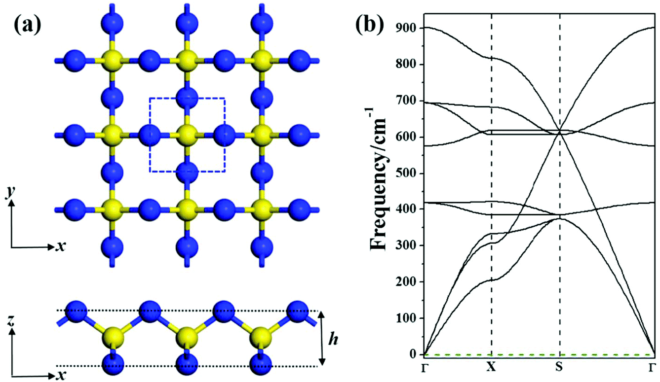 | ||
| Fig. 1 The S-SN2 monolayer: (a) optimized structure from top and side views (a 3 × 3 × 1 supercell, the unit cell is highlighted by the blue dashed square), blue and yellow balls denote N and S atoms, respectively; (b) computed phonon spectrum. | ||
The N–S bonds (d) of S-SN2 have the uniform length of 1.62 Å, and the layer thickness (h) is 1.88 Å, both shorter than those of the previously proposed 1T-SN2 monolayer (the d and h values are 1.80 and 1.90 Å, respectively, at the same level of theory). Note that structurally the S-SN2 monolayer well resembles the recently proposed monolayers of Tetra-MoN223 and CO2,24 and the orthorhombic SN2 (Pnnm) predicted by Li et al. can be considered as its bulk precursor.11 In the Pnnm-SN2 solid, the S atoms are hexa-coordinated and N atoms are tri-coordinated, the (0 0 1) slab can be viewed as the twisted S-SN2 monolayer.
Note that the sulfur atoms adopt the hexacoordinated and tetracoordinated states in the 1T-SN2 and S-SN2 monolayers, respectively. The hexacoordination of S was also realized in the dimeric N-chloroiminosulfur tetrafluoride.25 However, the tetracoordination of S, which was regarded to be only found in intermediates because of the strain,26 was barely obtained in experiment.27 It was recognized that usually electron-withdrawing groups such as F, O, and N are needed to stabilize the hypervalent state of sulfur.28 Thus, we expect that the 1T/S-SN2 monolayer containing the hexa/tetracoordinated S moiety is stabilized by the N atoms, each of which withdraws 0.19/0.23e− from S according to our Hirshfeld charge analysis.29
3.2. Stability of the S-SN2 monolayer
The intriguing structure of S-SN2 monolayer inspired us to further examine its stability. Firstly, we computed its cohesive energy (Ecoh), which is obtained by Ecoh = (nEN + mES − ESN2)/(n + m), where EN, ES and ESN2 are the total energies of a single N atom, a single S atom, and the SN2 monolayer, respectively. n and m are the number of N and S atoms in the supercell. According this definition, a material with a more positive Ecoh value has a higher thermodynamic stability. The cohesive energy of the S-SN2 monolayer is 3.24 eV per atom, larger than those of the 1T-SN2 monolayer (3.08 eV per atom) and the 3D SN2 crystal (2.68 eV per atom at 60 GPa),11 but smaller than the Ecoh value (3.45 eV per atom) of the cage-like S4N4 molecular crystal,30 the starting material for various synthetic routes in sulfur–nitrogen chemistry. In comparison, the cohesive energies of the experimentally realized 2D silicene31,32 and phosphorene33,34 are 3.54 and 3.48 eV per atom, respectively, at the same level of theory. The rather favorable cohesive energy of the S-SN2 monolayer ensures that it has a strongly connected network, and is very promising to be synthesized.Secondly, we confirmed that the S-SN2 monolayer is also dynamically stable, as demonstrated by the real frequency values in the phonon spectrum (Fig. 1b). The highest frequency is 900 cm−1, which is ∼50 cm−1 higher than that of 1T-SN2,14 and also higher than those of silicene (580 cm−1)35 and phosephorene (456 cm−1),36 indicating its remarkable dynamic stability.
Thirdly, we examined its thermal stability by performing first-principles molecular dynamics (FPMD) simulations with a 5 × 5 supercell. Our simulations at 300 K, 500 K, 1000 K, and 1500 K showed that the S-SN2 monolayer maintained its structural integrity throughout the 10 ps FPMD simulation up to 1000 K, but seriously distorted at 1500 K (Fig. S1†). The slightly distorted structure after the simulation at 1000 K can recover the initial configuration of S-SN2 monolayer upon full atomic relaxation. In comparison, the reported 1T-SN2 monolayer can also maintain the structural integrity up to 1000 K in our FPMD simulations (Fig. S2†), while the proposed S3N2 monolayer would dissociate into multiple S–N chains and clusters at the same high temperature.13
The above results demonstrate d that the S-SN2 monolayer is rather stable, and is expected to be experimentally feasible. Reminiscing the aromaticity in the ring structure of S2N2 and other sulfur–nitrogen molecules,3,37 the high stability of the S-SN2 monolayer raised another question: is the S-SN2 monolayer also aromaticity? To address this question, we examined the chemical bonding patterns of the S-SN2 monolayer by using the solid state adaptive natural density partitioning (SSAdNDP) method.38 The SSAdNDP results suggest that besides the two sp-orbital lone-pairs and two p-orbital lone-pairs on N atoms, there are four two-center-two-electron bonds between N and S in the unitcell of S-SN2 monolayer (Fig. S3†). As a result, the S-SN2 monolayer is not aromatic. Nevertheless, the sp2(N)–sp3(S) hybridization bonds lead to robust connection between the N and S atoms, and thus result in the pronouncing stability of 2D N–S network.
3.3. Electronic and optical properties of the S-SN2 monolayer
We further investigated the electronic properties of S-SN2 monolayer at the HSE06 level of theory. Similar to the 1T-SN2 monolayer, which has an indirect bandgap (Eg) of 2.89 eV according to our calculations (2.83 eV in the literature14), the S-SN2 monolayer is also an indirect-gap semiconductor with the bandgap of 2.79 eV (Fig. 2a). The valence band maxima (VBM) are mainly composed of p orbitals of nitrogen atoms, similar to the case of Tetra-MoN2,23a while the conduction band minima (CBM) consist of both S-p and N-p states (Fig. 2b and c).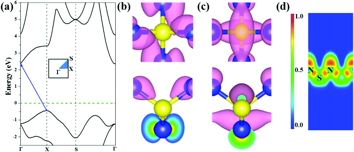 | ||
| Fig. 2 The S-SN2 monolayer: (a) band structure (the Fermi energy was set to be zero and denoted by the green dashed line), (b) spatial distributions of wave functions of VBM and (c) CBM from the top and side views (isovalue: 0.02 e Å−3); (d) ELF map sliced perpendicular to the 2D plane, red (ELF = 1) and blue (ELF = 0) indicate accumulated and vanishing electron density, respectively. | ||
To gain further insights into the chemical bonding of the S-SN2 monolayer, we examined the electron localization function (ELF), as visualized in Fig. 2d. Since the S atoms donate electrons to N atoms as suggested by the Hirshfeld charge analysis (0.23e− per N atom), the electron density around N atoms is rather localized with high ELF values. The electrons localized between S and N atoms show some deviation from the bond center, indicating the nature of polar covalent bonding, which partially contributes to the high thermal stability of the S-SN2 monolayer.
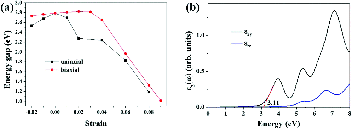
Since applying external strain is an effective way to engineer the band structures of 2D nanomaterials, we studied the effect of uniaxial and biaxial (tensile and compressive) strains (η) along x and y directions on the band structure of the S-SN2 monolayer, in comparison with the 1T-SN2 monolayer. During the uniaxial and biaxial strains, the dynamic stabilities of the S-SN2 monolayer could be reserved with η in the range of −2% ≤ η ≤ 8% and −2% ≤ η ≤ 9%, respectively. When the uniaxial (biaxial) strain of 9% (10%) or larger is imposed to the S-SN2 monolayer, imaginary frequencies will appear in the calculated phonon spectra (Fig. S4†), indicating that the dynamic instability of the monolayer under such extreme strains.
When the uniaxial strains (either compression or stretching) are applied to the S-SN2 monolayer, the bandgap decreases compared to that of the equilibrium structure (Fig. 3a). In particular, the uniaxial tensile strain could effectively decrease the bandgap: the value is reduced from the original 2.79 eV to 1.18 eV under uniaxial tensile of 8% (Fig. S5†). The uniaxial strains destroy the symmetry in the reciprocal space of the S-SN2 monolayer, and the CBM shifts down under both compression and expansion strains along the x-direction (remaining at Γ point for −2% ≤ η ≤ 7%, but switching to Y point for η = 8%), while the VBM oscillates around the X point, as a result, the bandgap is decreased regarding to the pristine Eg.
 | ||
| Fig. 3 (a) The HSE06 band gap as a function of the external strains for the S-SN2 monolayer. (b) The imaginary dielectric constants (the red dashed line denotes an approximate linear fitting for estimating the band edge of the first adsorption peak). | ||
In comparison, we examined the effect of uniaxial strain on the electronic structure of the 1T-SN2 monolayer. Interestingly, under the strain modulation, the 1T-SN2 monolayer remains the indirect-gap semiconducting nature. The band gap of 1T-SN2 exhibits a quasi-linear relation with the uniaxial strain in either x (armchair) or y (zigzag) direction (Fig. S5†): the band gap increases (decreases) monotonically with the tensile (compressive) strain along x direction, and the gap change is in a relative small range (2.82–2.96 eV) when the strain of −2% to 2% is applied; however, along y direction, the band gap decreases (increases) in a more pronounced manner with the tensile (compressive) strain. When the y-axial tensile strain is as large as 5%, the gap value reduces to 2.44 eV from 2.89 eV of the pristine monolayer; when the −2% compressive strain is imposed along the y direction, the gap is enlarged to 3.14 eV.
When applying biaxial strains to the S-SN2 monolayer in the range of −2%–3%, the bandgap increases almost linearly with increasing the strain (2.73–2.82 eV). When the tensile strain is even larger, at the external tensile of 4%, the bandgap drops from the linear relation, and the indirect-gap to direct-gap transition occurs (bandgap of 2.65 eV, Fig. S5†). Further increasing the strain continues to narrow the bandgap, but transits to indirect bandgap again, since the VBM moves from X/Y k-point for η = 4% to the value between X and Γ k-points for larger stretches, and under the biaxial tensile of 9%, the indirect bandgap of the S-SN2 monolayer is 1.01 eV. In comparison, the band gap of the 1T-SN2 monolayer decreases monotonically from ∼4.3 to ∼0.6 eV as the biaxial strain increases from −10% to 10%.14
Overall, the strain-tailored band structure of the S-SN2 monolayer can be contributed to the variation of the N–S bonds: the uniaxial or biaxial stretching weakens the N–S bonds, and as a result the CBM moves to lower energies and the bandgap was narrowed (Fig. S6†), which is in line with previous DFT finding that the strain effect on the band structures of boron nitride monolayers originates from the B–N bonding.39
Note that the S-SN2 monolayer is an indirect-gap semiconductor with the VBM and CBM located at the X and Γ points, respectively. This is beneficial to restrain the recombination of the photo-activated electron–hole pairs.40 Thus, we also investigated the optical adsorption property of the S-SN2 monolayer by computing the imaginary parts of the dielectric function ε2(ω). As shown in Fig. 3b, S-SN2 exhibits adsorption starting at ∼2.2 eV, and the optical gap (estimated by linear fitting of the first adsorption peak) is 3.11 eV, much smaller than that of 1T-SN2 (3.86 eV, Fig. S7†). Therefore, the S-SN2 monolayer might be used as the visible-light-driven photocatalysts.
3.4. Carrier mobility of the S-SN2 monolayer
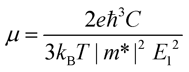
We then systematically investigated the carrier mobility of the S-SN2 monolayer to better understand its electronic properties using the deformation potential (DP) theory,41 which has been extensively applied to evaluate the carrier mobility of various 2D materials,34,42–49 and is derived from the following expression:where, ℏ is the reduced Planck constant, kB is the Boltzmann constant, T is the temperature (the room temperature 300 K was adopted in our study), m* is the effective mass in the transport direction, E1 and C are the DP constant and the in-plane stiffness, respectively. E1 signifies the shift of the band edges Eedge (VBM and CBM) induced by the strain δ (δ = Δa/ao, Δa and ao are the variation and equilibrium lattice lengths, respectively), with the form of E1 = ∂Eedge/∂δ. The in-plane stiffness can be determined by C = (∂2E/∂δ2)/So, where E is the total energy of the supercell, δ is the applied uniaxial strain, and So is the area of the equilibrium supercell.
The carrier mobility of the S-SN2 monolayer was evaluated along the x and y directions (Fig. 1a). The details of computing the in-plane stiffness C and the DP constant E1 are given in Fig. S6† and Table 1. The S-SN2 monolayer shows very high hole mobility of 1.16 × 103 cm2 V−1 s−1 for holes along both x and y directions, much higher than that of MoS2 (200 cm2 V−1 s−1);46 while the electron mobility (0.16 × 103 cm2 V−1 s−1) is comparable to those of black phosphorene (0.08 × 10³–1.14 × 103 cm2 V−1 s−1).45 In comparison, the 1T-SN2 monolayer has anisotropic carrier mobility along the x and y directions (Fig. S7 and 8†), and the electron mobility (∼2 × 103 cm2 V−1 s−1) is higher than those of holes (0.24 × 103 cm2 V−1 s−1 and 0.05 × 103 cm2 V−1 s−1 in x and y directions, respectively) in either direction, which is different from S-SN2, MoS2 and phosphorene with more mobile holes.45,46 The anisotropy of electron and hole mobilities was found in many 2D materials, such as the group 15 monolayers,50 the methyl-terminated germanene,51 8B-Pmmn borophene/borophane,52 and MXenes.53
| Carrier type |
|
|
|E1x| | |E1y| | C x | C y | μ x | μ y |
|---|---|---|---|---|---|---|---|---|
| (eV) | (J m−2) | (103 cm2 V−1 s−1) | ||||||
| Electron | 0.47 | 10.43 | 279.82 | 0.16 | ||||
| 0.80 | 0.28 | 1.79 | 4.76 | 242.20 | 242.20 | 1.67 | 1.87 | |
| Hole | −2.46 | 0.75 | 279.82 | 1.16 | ||||
| −0.88 | −1.36 | 4.26 | 6.33 | 242.20 | 242.20 | 0.24 | 0.05 | |
3.5. Mechanical properties of the S-SN2 monolayer
Besides the electronic properties, we also investigated the mechanical properties of the S-SN2 monolayer by examining the elastic constants. The computed elastic constants of graphene are C11 = C22 = 351.77 N m−1 and C12 = C21 = 60.13 N m−1, which are in good agreement with previous experimental measurements54 and computational results.55 For the S-SN2 monolayer, the computed elastic constants are C11 = C22 = 282.89 N m−1, C12 = C21 = −29.50 N m−1, and C44 = 10.34 N m−1. Based on the mechanical stability criteria (C11C22 − C122 > 0, C44 > 0),56 the S-SN2 monolayer is mechanically stable and isotropic: it has a negative in-plane Poisson's ratio of −0.104 (C12/C11) for both x and y directions, and a high in-plane Young's modulus ((C11C22 − C12C21)/C22) of 279.82 N m−1, larger than those of 1T-SN2 (242.20 N m−1) and MoS2 (124.06 N m−1) monolayers at the same level of theory.To confirm the unusual negative Poisson's ratio (NPR), we examined a series of uniaxial tensile strains as illustrated in Fig. 4. When elongating along x direction by δx (1% ≤ δx ≤ 5%) of the S-SN2 monolayer, expansions in both the in-plane y direction and the out-of-plane z direction were found as indicated by the positive resultant strains along y and z directions (δy and δz). More specifically, the resultant strain δy increases monotonically from 0.85% to 1.34% when the applied tensile δx enhances from 1% to 6%; while the resultant δz decreases from 1.46% to 0.11% when δx is increased from 1% to 5%, and the δz value decreases to a negative value of −0.33% when δx reaches 6%. The coexistence of the out-of-plane NPR and the in-plane NPR suggests that the S-SN2 monolayer is new family member of 2D monolayers with 3D auxetic properties following the just predicted S3N2 monolayers with α-heart structure (whose in-plane NPR is −0.026, much smaller than the corresponding value −0.104 of the S-SN2).57
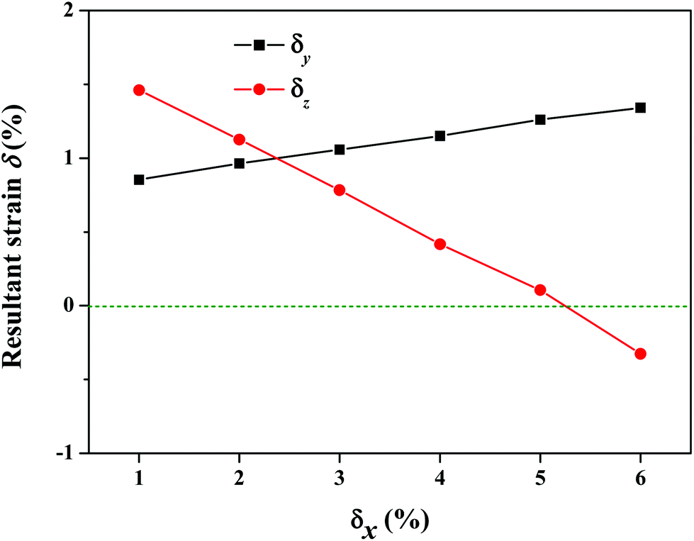 | ||
| Fig. 4 Mechanical response of the S-SN2 monolayer under uniaxial tensile strain along x direction. | ||
3.6. The S-SN2 bilayers
Thickness and stacking pattern were also examined to get further insights into the electronic properties of S-SN2, since they can affect the properties of 2D materials.40c,58 Two possible stacking patterns of S-SN2 bilayer, namely AA and AB stackings, were considered (Fig. S9†). In comparison, we also examined the stacking patters of the 1T-SN2 bilayer (four patterns, AA, AA′, AB, and AB′, Fig. S10†).The interlayer distances (4.55 and 4.81 Å for AA and AB stacking, respectively) of the S-SN2 bilayers are larger than those of 1T-SN2 bilayers (2.95–3.07 Å, Table S1†). The binding energy (Eb) of the SN2 bilayer in different stacking configurations is calculated via Eb = (2 × Emonolayer − Ebilayer)/2, where Emonolayer and Ebilayer are the total energies of the SN2 monolayer and bilayer, respectively. The binding energies of the S-SN2 bilayers (0.30 and 0.29 eV for AA and AB stacking, respectively) are comparable to or slightly higher than those of 1T-SN2 bilayers (0.28–0.29 eV, Table S1†).
As expected, the bandgaps of S-SN2 bilayer in AA and AB stacking configurations are respectively reduced to 2.64 and 2.60 eV (Fig. S9†) compared to that of the monolayer (2.79 eV), the S-SN2 bulk in the AA stacking remains being indirect semiconducting but with a further reduced band gap of 2.58 eV.
Similarly, the indirect bandwidth of 1T-SN2 bilayer was narrowed compared to that of monolayer: 2.76 and 2.69 eV for the AB and AA stacking, respectively. Since the band gap is more sensitive in the AA stacking pattern and the stability of AA stacking is very close to the AB stacking for 1T-SN2 bilayer, we further computed the electronic structures of the 1T-SN2 trilayer and tetralayer in AA stacking (Fig. S11†). The band gap turns to be 2.59 and 2.54 eV, respectively, and the 1T-SN2 bulk in AA stacking has an indirect bandgap of 2.28 eV.
4. Conclusion
In summary, we predicted a new phase of SN2 monolayer, namely S-SN2, by using first-principles calculations combined with the particle-swarm optimization method. Its structure belongs to space group PM2 and features the unusual tetracoordinated S. The moderate cohesive energy, absence of imaginary modes in phonon spectrum, and structural integrity through 10 ps FPMD simulations up to 1000 K indicate the high stability of the S-SN2 monolayer. The S-SN2 monolayer is an indirect-bandgap semiconductor with high hole mobilities, and shows adsorption in the visual-light region. The bandgap of the S-SN2 monolayer can be further tuned by thickness and external strains, and an indirect–direct bandgap transition could be induced under the biaxial tensile strain. Moreover, it has large Young's modulus, and the coexistence of out-of-plane and in-plane negative Poisson's ratios renders the S-SN2 monolayer 3D auxetic properties. Therefore, the S-SN2 monolayer is expected to have wide applications in electronics, photoelectronics, and mechanics. Especially, we are calling for more efforts in developing 2D crystals with 3D auxetic properties, which will bring us more breakthroughs in materials with novel Poisson's ratio materials.
Conflicts of interest
There are no conflicts of interest to declare.Acknowledgements
This work was financially supported in China by the National Natural Science Foundation of China (No. 11464032, 11828401, 21103224) and the Startup Project of Inner Mongolia University (21200-5175101), and in USA by NSF-CREST Center for Innovation, Research and Education in Environmental Nanotechnology (CIRE2N) (Grant Number HRD-1736093). Most computations were carried out in PARATEAR at Guangzhou Supercomputer Center, and part of this research used resources of the High Performance of Computational facility (HPCf), University of Puerto Rico, which is partially supported by an Institutional Development Award (IDeA) INBRE Grant Number P20GM103475 from the National Institute of General Medical Sciences (NIGMS), a component of the National Institutes of Health (NIH), and the Bioinformatics Research Core of the INBRE. Its contents are solely the responsibility of the authors and do not necessarily represent the official view of NIH.References
- (a) T. Chivers, Chem. Rev., 1985, 85, 341–365 CrossRef CAS; (b) T. Chivers, A Guide to Chalcogen-Nitrogen Chemistry, World Scientific,Singapore, 2005, p. 334 CrossRef; (c) T. Chivers, Sulfur–Nitrogen Compounds, in Encyclopedia of Inorganic and Bioinorganic Chemistry, John Wiley & Sons, Ltd., 2011, DOI:10.1002/9781119951438.eibc0214.
- (a) F. X. Powell, Chem. Phys. Lett., 1975, 33, 393–395 CrossRef CAS; (b) S. Sensarma and A. G. Turner, Inorg. Chim. Acta, 1982, 64, L161–L162 CrossRef CAS; (c) S. R. Kass and C. H. DePuy, J. Org. Chem., 1985, 50, 2874–2877 CrossRef CAS; (d) C. Wentrup, S. Fischer, A. Maquestiau and R. Flammang, J. Org. Chem., 1986, 51, 1908–1910 CrossRef CAS; (e) H. Bender, F. Carnovale, J. B. Peel and C. Wentrup, J. Am. Chem. Soc., 1988, 110, 3458–3461 CrossRef CAS; (f) R. D. Brown, P. S. Elmes and D. McNaughton, J. Mol. Spectrosc., 1990, 140, 390–400 CrossRef CAS; (g) R. D. Davy and H. F. Schaefer III, J. Am. Chem. Soc., 1991, 113, 1917–1922 CrossRef CAS; (h) T. Chivers, P. W. Codding and R. T. Oakley, J. Chem. Soc., Chem. Commun., 1981, 584–585 RSC.
- (a) Y. Jung, T. Heine and P. v. R. Schleyer, J. Am. Chem. Soc., 2004, 126, 3132–3138 CrossRef CAS; (b) F. De Proft, P. W. Folwer, R. W. A. Havenith, P. v. R. Schleyer, G. Van Lier and P. Geerlings, Chem. – Eur. J., 2004, 10, 940–950 CrossRef CAS.
- P. Hassanzadeh and L. Andrews, J. Am. Chem. Soc., 1992, 114, 83–91 CrossRef CAS.
- M. J. Cohen, C. M. Mikulski, A. F. Garito, A. J. Heeger, A. G. MacDiarmid, M. S. Saran and J. Kleppinger, J. Am. Chem. Soc., 1976, 98, 3844–3848 CrossRef CAS.
- R. W. H. Small, A. J. Banister and Z. V. Hauptman, J. Chem. Soc., Dalton Trans., 1981, 2188–2191 RSC.
- B. G. Kumar and K. Muralidharan, RSC Adv., 2014, 4, 28219–28224 RSC.
- T. Chivers and J. Proctor, Can. J. Chem., 1979, 57, 1286–1293 CrossRef CAS.
- M. Boudeulle, Cryst. Struct. Commun., 1975, 4, 9–13 CAS.
- R. L. Greene, P. M. Grant and G. B. Street, Phys. Rev. Lett., 1975, 34, 89–92 CrossRef CAS.
- D. Li, F. Tian, Y. Lv, S. Wei, D. Duan, B. Liu and T. Cui, J. Phys. Chem. C, 2017, 121, 1515–1520 CrossRef CAS.
- D. Laniel, M. Bykov, T. Fedotenko, A. V. Ponomareva, I. A. Abrikosov, K. Glazyrin, V. Svitlyk, L. Dubrovinsky and N. Dubrovinskaia, Inorg. Chem., 2019, 58, 9195–9204 CrossRef CAS.
- H. Xiao, X. Shi, X. Liao, Y. Zhang and X. Chen, Phys. Rev. Mater., 2018, 2, 024002 CrossRef CAS.
- J.-H. Lin, H. Zhang, X.-L. Cheng and Y. Miyamoto, Phys. Rev. B: Condens. Matter Mater. Phys., 2016, 94, 195404 CrossRef.
- J. P. Perdew, K. Burke and M. Ernzerhof, Phys. Rev. Lett., 1996, 77, 3865–3868 CrossRef CAS.
- P. E. Blöchl, Phys. Rev. B: Condens. Matter Mater. Phys., 1994, 50, 17953–17979 CrossRef.
- G. Kresse and J. Furthmüller, Phys. Rev. B: Condens. Matter Mater. Phys., 1996, 54, 11169–11186 CrossRef CAS.
- T. Bučko, J. Hafner, S. Lebègue and J. G. Ángyán, J. Phys. Chem. A, 2010, 114, 11814 CrossRef PubMed.
- H. J. Monkhorst and J. D. Pack, Phys. Rev. B: Solid State, 1976, 13, 5188–5192 CrossRef.
- J. Heyd, G. E. Scuseria and M. Ernzerhof, J. Chem. Phys., 2003, 118, 8207–8215 CrossRef CAS.
- G. J. Martyna, M. L. Klein and M. E. Tuckerman, J. Chem. Phys., 1992, 97, 2635–2643 CrossRef.
- Y. Wang, J. Lv, L. Zhu and Y. Ma, Phys. Rev. B: Condens. Matter Mater. Phys., 2010, 82, 094116 CrossRef.
- (a) C. Zhang, J. Liu, H. Shen, X.-Z. Li and Q. Sun, Chem. Mater., 2017, 29, 8588 CrossRef CAS; (b) Y. Wang and Y. Ding, J. Mater. Chem. C, 2018, 6, 2245–2251 RSC.
- S. Liu, H. Du, G. Li, L. Li, X. Shi and B. Liu, Phys. Chem. Chem. Phys., 2018, 20, 20615–20621 RSC.
- A. Waterfeld and R. Mews, Angew. Chem., Int. Ed. Engl., 1981, 20, 1017 CrossRef.
- B. K. Ackerman, K. K. Andersen, I. Karup-Nielsen, N. B. Peynircioglu and S. A. Yeager, J. Org. Chem., 1974, 39, 964–968 CrossRef CAS.
- (a) K. D. Schmidt, R. Mews and O. Glemser, Angew. Chem., Int. Ed. Engl., 1976, 15, 614–615 CrossRef; (b) H. W. Roesky, M. Witt, B. Krebs and H. Korte, Angew. Chem., Int. Ed. Engl., 1979, 18, 415 CrossRef.
- N. Kano, Y. Itoh, Y. Watanabe, S. Kusaka and T. Kawashim, Angew. Chem., Int. Ed., 2008, 47, 9430–9433 CrossRef CAS.
- F. L. Hirshfeld, Theor. Chim. Acta, 1977, 44, 129–138 CrossRef CAS.
- S. C. Abrahams, Acta Crystallogr., Sect. B: Struct. Sci., 1996, 52, 790–805 CrossRef.
- B. J. Feng, Z. Ding, S. Meng, Y. Yao, X. He, P. Cheng, L. Chen and K. Wu, Nano Lett., 2012, 12, 3507–3511 CrossRef CAS.
- A. Fleurence, R. Friedlein, T. Ozaki, H. Kawai, Y. Wang and Y. Yamada-Takamura, Phys. Rev. Lett., 2012, 108, 245501 CrossRef.
- L. Li, Y. Yu, G. J. Ye, Q. Ge, X. Ou, H. Wu, D. Feng, X. H. Chen and Y. Zhang, Nat. Nanotechnol., 2014, 9, 372–377 CrossRef CAS.
- H. Liu, A. T. Neal, Z. Zhu, D. Tomanek and P. D. Ye, ACS Nano, 2014, 8, 4033–4041 CrossRef CAS.
- S. Cahangirov, M. Topsakal, E. Akturk, H. Sahin and S. Ciraci, Phys. Rev. Lett., 2009, 102, 236804 CrossRef CAS.
- R. Fei and L. Yang, Appl. Phys. Lett., 2014, 105, 083120 CrossRef.
- M. Springborg, Int. Rev. Phys. Chem., 1993, 12, 241–303 Search PubMed.
- T. R. Galeev, B. D. Dunnington, J. R. Schmidt and A. I. Boldyrev, Phys. Chem. Chem. Phys., 2013, 15, 5022–5029 RSC.
- Q. Pang, L. Liu and J. Zhao, J. Appl. Phys., 2017, 122, 094302 CrossRef.
- (a) H. Zhang, L. Liu and Z. Zhou, Phys. Chem. Chem. Phys., 2012, 14, 1286–1292 RSC; (b) H. Zhang, L. Liu and Z. Zhou, RSC Adv., 2012, 2, 9224–9229 RSC; (c) H. Zhang, Y. Yang, Z. Zhou, Y. P. Zhao and L. Liu, J. Phys. Chem. C, 2014, 118, 14662–14669 CrossRef CAS; (d) H. Zhang, X. Q. Zuo, H. B. Tang, G. Li and Z. Zhou, Phys. Chem. Chem. Phys., 2015, 17, 6280–6288 RSC; (e) H. Zhang, G. Tang, X. Zuo, H. Tang, Q. Yang and G. Li, J. Mater. Chem. A, 2016, 4, 12913–12920 RSC.
- J. Bardeen and W. Shockley, Phys. Rev., 1950, 80, 72–80 CrossRef CAS.
- M.-Q. Long, L. Tang, D. Wang, L. Wang and Z. Shuai, J. Am. Chem. Soc., 2009, 131, 17728–17729 CrossRef CAS.
- M. Long, L. Tang, D. Wang, Y. Li and Z. Shuai, ACS Nano, 2011, 5, 2593–2600 CrossRef CAS.
- S. Bruzzone and G. Fiori, Appl. Phys. Lett., 2011, 99, 222108 CrossRef.
- J. Qiao, X. Kong, Z.-X. Hu, F. Yang and W. Ji, Nat. Commun., 2014, 5, 4475 CrossRef CAS.
- Y. Cai, G. Zhang and Y. W. Zhang, J. Am. Chem. Soc., 2014, 136, 6269–6275 CrossRef CAS.
- X. Zhang, X. Zhao, D. Wu, Y. Jing and Z. Zhou, Nanoscale, 2015, 7, 16020–16025 RSC.
- Y. Jing, X. Zhang, D. H. Wu, X. D. Zhao and Z. Zhou, J. Phys. Chem. Lett., 2015, 6, 4252–4258 CrossRef CAS.
- M. Xie, S. Zhang, B. Cai, Y. Huang, Y. Zou, B. Guo, Y. Gu and H. Zeng, Nano Energy, 2016, 28, 433–439 CrossRef CAS.
- S. Zhang, M. Xie, F. Li, Z. Yan, Y. Li, Z. Chen and H. Zeng, Angew. Chem., Int. Ed., 2016, 55, 1666–1669 CrossRef CAS.
- Y. Jing, X. Zhang, D. Wu, X. Zhao and Z. Zhou, J. Phys. Chem. Lett., 2015, 6, 4252–4258 CrossRef CAS PubMed.
- T. Cheng, H. Lang, Z. Li, Z. Liu and Z. Liu, Phys. Chem. Chem. Phys., 2017, 19, 23942–23950 RSC.
- H. Lang, S. Zhang and Z. Liu, Phys. Rev. B: Condens. Matter Mater. Phys., 2016, 94, 235306 CrossRef.
- C. G. Lee, X. D. Wei, J. W. Kysar and J. Hone, Science, 2018, 321, 385–388 CrossRef.
- X. Li, Q. Zhang and Q. Wang, Phys. Chem. Chem. Phys., 2013, 15, 7142–7146 RSC.
- Y. Ding and Y. Wang, J. Phys. Chem. C, 2013, 117, 18266–18278 CrossRef CAS.
- Y. Chen, X. Liao, X. Shi, H. Xiao, Y. Liu and X. Chen, Phys. Chem. Chem. Phys., 2019, 21, 5916–5924 RSC.
- T. Ohta, A. Bostwick, J. L. McChesney, T. Seyller, K. Horn and E. Rotenberg, Phys. Rev. Lett., 2007, 98, 206802 CrossRef PubMed.
Footnotes |
| † Electronic supplementary information (ESI) available. See DOI: 10.1039/c9nr07263b |
| ‡ Equal contribution to this work. |
| This journal is © The Royal Society of Chemistry 2020 |