
Recent progress in controlled nano/micro cracking as an alternative nano-patterning method for functional applications
Jinwook
Jung†
a,
Kyun Kyu
Kim†
a,
Young. D.
Suh
a,
Sukjoon
Hong
b,
Junyeob
Yeo
*c and
Seung Hwan
Ko
 *ade
*ade
aApplied Nano and Thermal Science Lab, Department of Mechanical Engineering, Seoul National University, 1 Gwanak-ro, Gwanak-gu, Seoul, 08826, Republic of Korea. E-mail: maxko@snu.ac.kr
bNovel Applied Nano Optics Lab, Department of Physics, Kyungpook National University, 80 Daehak-ro, Bukgu, Daegu 41566, Republic of Korea
cDepartment of Mechanical Engineering, Hanyang University, 55 Hanyangdaehak-ro, Sangnok-gu, Ansan, Gyeonggi-do 15588, Republic of Korea. E-mail: junyeob@knu.ac.kr
dInstitute of Advanced Machines and Design (IAMD), Seoul National University, Seoul 08826, Republic of Korea
eInstitute of Engineering Research, Seoul National University, Seoul 08826, Republic of Korea
First published on 29th May 2020
Abstract
Generally, cracking occurs for many reasons connected to uncertainties and to the non-uniformity resulting from intrinsic deficiencies in materials or the non-linearity of applied external (thermal, mechanical, etc.) stresses. However, recently, an increased level of effort has gone into analyzing the phenomenon of cracking and also into methods for controlling it. Sophisticated manipulation of cracking has yielded various cutting-edge technologies such as transparent conductors, mechanical sensors, microfluidics, and energy devices. In this paper, we present some of the recent progress that has been made in controlling cracking by giving an overview of the fabrication methods and working mechanisms used for various mediums. In addition, we discuss recent progress in the various applications of methods that use controlled cracking as an alternative to patterning tools.
1. Introduction
Crack propagation in materials can be generally explained by the energy balance between the energy absorbed during the production of new cracks and the strain energy that is released from the region to become unloaded.1 Cracks will propagate further around pre-existing voids and defects when the stress due to various external factors (mechanical forces,2,3 thermal stress,4,5 or capillary forces6,7) exceeds a critical point. Critical-cracking stress is dependent on various material characteristics such as the initial void/grain size, modulus, and surface energy. Moreover, the applied stress varies from area to area and depends on the mechanical (notch or void)8,9 and chemical structure (chemical bonding and interfaces between two materials)10–12 of the material. Therefore, it is difficult to predict the propagation of a particular crack and, because of their inherent randomness, cracks are generally considered to be a type of structural failure or an unwanted pattern to be excluded during the fabrication of a device.13–17 However, in 1993, A. Yuse successfully showed how to control cracking on glass substrates by cooling them rapidly after heating to allow the stress to accumulate.18 Around the same time, the controlled cracking of a dried colloidal suspension was described by C. Allain et al. They produced regular crack patterns in a dried film by the directional drying of a colloidal suspension within a confined geometry. Inspired by these studies, various other fundamental studies related to cracking control have followed over the last two decades.19Before 2010, no techniques utilizing cracks as a functional application had emerged, and the majority of these studies concentrated on theoretical analysis. Since then, technologies related to controlling cracking have yielded novel methods that have achieved unprecedented functionality. These methods provide a viable way of rapidly generating pattern sizes ranging from a few nanometers to a few micrometers over a large area, while the width and density of the patterns can be easily adjusted using a different medium, various structures, and stress control. These attempts have yielded new studies into methods for effectively manipulating sophisticated nano-scale structures that are difficult to produce using conventional lithography. Accordingly, recent developments have produced powerful solutions that can be used as an alternative to patterning tools in a wide range of applications such as optoelectronics, semiconductor devices, energy devices, and microfluidics.
In this article, we examine the advances that have been made in controlling cracked structures, and further explore various functional applications that use controlled cracking. The fabrication methods used to produce controlled cracking and the physical features of cracks (crack width, shape, and density) vary a lot depending on the medium and inducing forces. Therefore, we focus on recent functional applications that use controlled cracking as an alternative to patterning tools, in particular, and categorize these applications into three main approaches: transparent conductors, functional sensors, and other applications (including crack lithography, microfluidics, and three-dimensional structure fabrication). These approaches also include the fabrication methods used to produce controlled cracking and the working mechanisms used in various mediums.
2. Fabrication methods used to produce controlled cracking
This section will cover the representative fabrication methods used to produce controlled cracking in different mediums, including the progress that has been made in crack initiation and termination methods.2.1 Cracking by inducing stresses in different mediums
Cracks occur when the accumulated stress inside a medium exceeds a critical value, and this stress usually has its origin in external factors such as thermal stress,18,20 mechanical stress,21,22 evaporation-induced stress,19,23,24 solidification-induced stress,25,26 and environmental stress.27Thermal-induced cracking is a commonly used method of controlling cracks since it is easily applicable to conventional MEMS processing or top-down lithography;28–30 it is commonly used with inorganic materials such as glass or ceramic.31,32 In the earliest research into thermal-induced cracks by A. Yuse, the stress was generated at the end of the glass substrate by repeated, rapid heating and cooling.18 By controlling the speed of the substrate's movement, cracks were initiated on the edge of the glass substrate as a result of the highly anisotropic temperature field.
External mechanical stresses are also actively used to form cracks in multi-layered materials, which are usually composed of rigid materials and flexible/stretchable substrates, such as platinum deposited on polyurethane acrylate (PUA) film or an oxidized silica-like layer formed on polydimethylsiloxane (PDMS) elastomer.33 When external mechanical stresses are applied to these structures by bending or stretching, tensile stresses are formed in the rigid layer and cracks are induced. The crack density can be controlled by adjusting various parameters such as the film thickness or amount of induced stress.
In the case of colloidal suspensions, cracks also appear due to the evaporation of solvents. During the evaporation of the solvents, the colloidal assembly shrinks and a tensile stress is thereby developed. The features of the cracks can be controlled by adjusting various parameters such as the colloidal film thickness and drying speed in order to produce smaller cracks with narrower spacings.34,35 Furthermore, low-adhesive substrates reduce the cracking as the pinning effect of the colloidal suspension on these substrates is lower.
During the solidification of materials, internal stresses can appear. For example, in the welding processing of metal, the volume of metal in the liquid phase shrinks during solidification and cooling, and the induced stress contributes to the formation of solidification cracks. In addition to metals, it has been reported that the cross-linking of UV-curable resin induces volume shrinkage, which produces internal stress.25
Unlike other types of stress, environmental stress usually acts as a surface agent that alters the surface condition of materials, thus lowering the critical point for crack generation or propagation rather than producing cracks directly. Environmental stresses mainly focused on polymer materials that are easily affected by humidity, water, or various chemicals. There are various theories that try to explain this phenomenon. One such theory relates to the diffusion of liquid agents into polymers. Swollen polymers have increased chain mobility, and, thus, deformation can easily occur at relatively low levels of stress.36,37 Another theory is that wetting by the liquid reduces the energy needed to produce free surfaces in the polymer by cracking, thereby helping the formation of cracks.38,39
2.2 Crack generation and direction control using the initiation method
As mentioned above, cracks can be initiated at the edge of a piece of glass by rapidly quenching the heated glass substrate18,40 (Fig. 1a). Similarly, in colloidal suspensions, cracks can be controlled through directional evaporation. When a solvent evaporates, the two opposing phenomena of stress relaxation and accumulation lead to the formation of an ordered array of cracks. Stress relaxation occurs when the crack is generated, and these cracks induce further stress accumulation through evaporation at the generated crack surfaces. After the initial crack generation, secondary cracks are generated by strong capillary stresses that arise when the solvent completely evaporates (Fig. 1b).41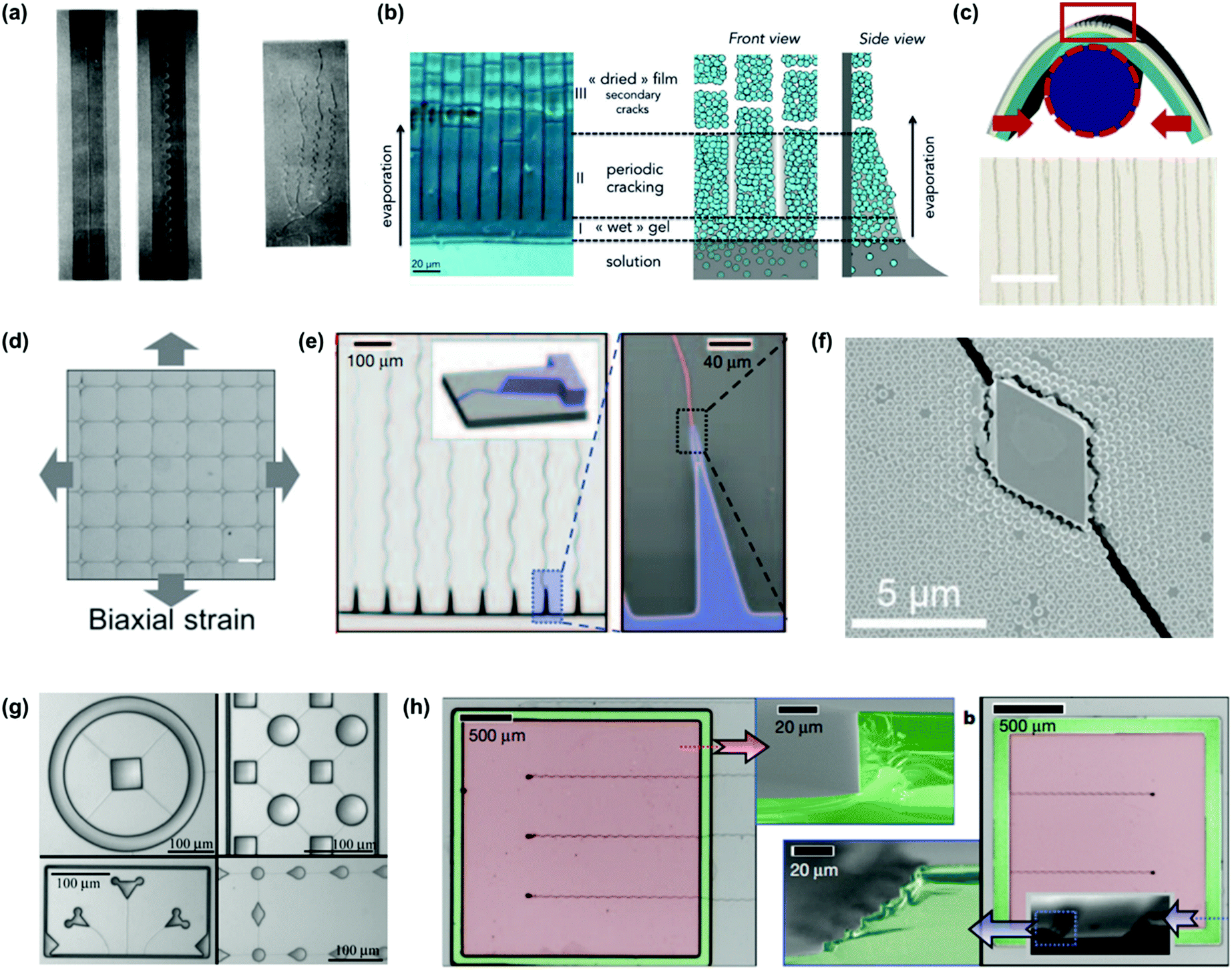 | ||
| Fig. 1 Different crack-control methods. Cracks generated by (a) thermal stress,40 (b) directional solvent evaporation,41 and (c) external mechanical force.33 Notch structures can successfully control the crack initiation point induced by (d) external mechanical force,42 (e) thermal stress,8 and (f) solvent evaporation.46 For the termination of crack propagation, (g) free edges48 or (h) stepped patterns8 can be used. | ||
In the case of a crack generated by external mechanical stress, the crack pattern tends to vertically align with the given tensile stress direction (Fig. 1c).33 If a pre-arranged notch structure is introduced into the structure, cracks appear only at the notches where stresses can be easily concentrated (Fig. 1d).42–44 Uncontrolled random cracks are not observed in this situation since the cracks generated at the notches release the nearby accumulated stresses.
Notched structures are more commonly used in the MEMS-based crack-control technique. Generally, the MEMS-based method relies mainly on the thermal stress, and the cracking initiates from the edge of the wafer, which is subject to residual stress due to effective heat release. The notch structure produces additional surfaces, resulting in a local stress concentration that reaches the critical value earlier than other regions; thus, the cracks tend to initiate from the notch structures rather than the edge of the substrates.8 This type of situation is depicted in Fig. 1e. Meanwhile, cracks can easily appear in narrow, V-shaped notches due to the concentrated stress. However, it is crucial to optimize precise notch-manipulation techniques since these structures may cause the generation of multiple uncontrollable cracks.45
Notch structures also affect substrates with colloidal suspensions, where colloidal crystals form after the evaporation of the solvents. Cracking of the colloidal crystal is selectively initiated from the notch structures,46 as shown in Fig. 1f. Moreover, the crack density and depth can be varied by simply altering the thickness of the material.47 Since the crack depth and density trend in opposite directions with increasing layer thickness, researchers have manipulated the crack density using this method as a performance-controlling tool for crack-based mechanical sensors.
2.3 Crack termination method
A crack termination method is essential for a more sophisticated crack patterning. In general, the easiest method for crack termination is to place free edges in the direction of the crack propagation (Fig. 1g)48 the initial crack will then terminate perpendicularly at the free surfaces.8,48,49 However, in some cases, single-step structures are not sufficient to terminate the crack propagation since the structure is not sufficient to release the whole of the accumulated stress. In order to improve these structures, K. Nam et al. successfully terminated the propagation of cracking in Si3N4 films on Si wafers using a stepped pattern that was made by photo-lithography (Fig. 1h). Using this method, letters consisting solely of generated cracks could be written. An improvement of this technique, a manual nano-fabrication method that used a cracking termination structure, has also been presented.50 In manual nano-fabrication methods, crack termination structures are fabricated in advance; the crack propagation is then terminated at the pre-patterned structures. The studies mentioned above have been influential on later studies and provide an alternative way as a patterning tool since the control of cracking is realized using the initiation and termination points. Likewise, in polymeric materials such as SU-8, cracks initiating from V-shaped notches can be terminated by introducing round notch structures that successively reduce the stress. In addition to the notch structures, secondary exposure of UV light increases the fracture stress in SU-8 and, in this way, the crack patterning can be more precisely controlled.49,51By controlling the initiation and termination points of cracking simultaneously, the controlled cracking technique offers great potential as an alternative pattering tool and nano-fabrication process that has a wide range of applications, such as transparent conductors and functional sensors. Attempts to utilize the advantages of crack-control methods and to develop functional applications have increased dramatically since the early 2010s. Controlled cracking is applied in transparent conductors as a large-area patterning template and provides an efficient replacement for conventional lithography processes. In addition, functional sensors are fabricated by using controlled cracking as an alternative way of producing unique nano-scale patterns as this is not easy to do using conventional fabrication processes. The recent progress and developments in functional applications using controlled cracking will be discussed in the following sections.
3. Transparent conductors
The importance of transparent conducting electrodes (TCEs) to large-area displays and in opto-electrical applications is continuously increasing,52 and the use of crack templates can be highly effective for the fabrication of transparent random metal-grid conductors. In common with metal-grid TCEs, TCEs produced using crack templates have the advantages of having easily controllable optical properties together with high a figure-of merit (FoM).34,53 They also have seamless junctions, which give a low contact resistance between conducting wires54 and superior transmittance over a broad wavelength range,55,56 while the random nature of the crack-based structure yields additional advantages. The irregular shapes of the electrical networks produced in this way help to ensure that the TCEs are free of Moiré patterns57,58 and that the products can be easily produced even on irregular substrates that are not compatible with the conventional photolithography processes used for regular metal-grid conductors.34 In addition, the non-periodicity of the conducting network does not affect the performance of the overall TCE significantly, as has been confirmed by various theoretical and experimental approaches.59For most of the relevant studies, the fabrication of a TCE using a crack template can generally be summarized as consisting of the following four steps:60 (1) preparation of a dispersion or gel film, (2) self-cracking, (3) deposition of a metallic film, and (4) removal of the template film. These steps are summarized in Fig. 2a. There is a range of cracking films available: specific examples include acrylic resin,34,35 SiO2 nanoparticle-based dispersion,61 microcrystalline TiO2 solution,60 Si3N4 layer on Si wafer,57,58,62 and egg white.53 The details of the cracking mechanism may differ, but it is known that the interfacial stress resulting from the adhesive force between particles, or between particles and the substrate after drying, plays an important role.56 As a result, the properties of the cracking template, e.g. the crack spacing and crack width, are not only dependent on the cracking material but also on various physical properties of the prepared film and the drying conditions.55 The type of cracking material itself does not directly affect the performance of the TCE that is produced since it is only utilized as a sacrificial layer; however, it should be noted that the induced cracks have to be connected to each other and the underlying substrate to create a highly conducting and mechanically robust TCE with good adhesion to the substrates.56 These cracks are often termed ‘crackle’ to emphasize these features.35,55,56 From the perspective of the process, the preparation of the cracking film is achieved by spin coating,60 drop coating,56 rod coating,54 and spray coating.34 Among the aforementioned processes, spray coating possesses the unique advantage that it is directly applicable to an arbitrary or irregular structure such as a glass tube and convex lens34 (Fig. 2b).
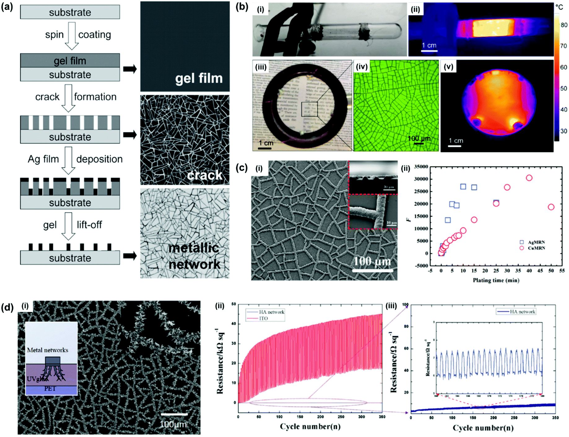 | ||
| Fig. 2 Cracked template based transparent conductors. (a) General fabrication steps for crack-template based TCE.60 (b) Cracked template based TCE fabricated by spray coating on a tube (i, ii) and a convex lens (iii, iv, v).34 (c) Metallic network TCE after the electroplating and the change in figure-of-merit.53 (d) Bamboo root inspired metallic network and its enhanced mechanical adhesion.67 | ||
Either evaporation or sputtering can be employed for the metallic film deposition,60 and various metals, including Au, Ag, Cu, Pd, Al, and Zn, are available56 for use as metallic TCEs; however, Ag and Cu are the most widely used.53,54,62,63 By successive deposition of different metals, a hybrid wire network composed of heterogeneous metals can also be created in order to tune the electrical properties of the TCE for control of the passivation and work functions.56 However, these conventional metal deposition techniques increase the overall complexity of the fabrication process as they require a vacuum environment, and so non-vacuum approaches have been investigated as a substitute for these vacuum deposition techniques. Electroless deposition or electroplating is a well-known approach used to create metallic structures that does not require a vacuum environment; however, it does require the use of specific substrates or the separate nucleation of seed nanoparticles within the crackle region.54 The creation of a seed layer can often incorporate vacuum techniques,53 but the use of specific materials such as the commercial amorphous fluoropolymer CYTOP eliminates the need for sputtering or evaporation.64 Once a proper seed layer is ready, specific metals can be generated within the crackle region whereas the morphology of the resulting metallic line is dependent on the electroplating time.53 By increasing the electroplating time, the metallic line will become more semicircular, and very high electrical conductivity can be achieved at the expense of network visibility and haze; however, such properties are actually rather desirable in the case of solar cells and high-power light-emitting diodes. Minute control of electroplating can thus create metallic TCEs with very high FoMs of 30![[thin space (1/6-em)]](https://www.rsc.org/images/entities/char_2009.gif) 000 or even higher63 (Fig. 2c). As well as electroless deposition or electroplating, the generation of a metallic region using vacuum-free techniques has been proposed by Suh et al. – in this case, using metal nanoparticles (NPs)62 or nanowires (NWs)57 that selectively fill the crackle region. The metal NPs and NWs in the crackle region are then transferred to the target substrate using UV epoxy resin; in addition, laser sintering is also used in order to enhance their electrical conductivity as well as the adhesion to the substrate. These methods differ from other crack-template TCEs in that the crack template is not used sacrificially and thus can be reused. In other cases, after the metal deposition, the crack template has to be removed by cleaning with a specific solvent56 or by using ultrasound in water.61
000 or even higher63 (Fig. 2c). As well as electroless deposition or electroplating, the generation of a metallic region using vacuum-free techniques has been proposed by Suh et al. – in this case, using metal nanoparticles (NPs)62 or nanowires (NWs)57 that selectively fill the crackle region. The metal NPs and NWs in the crackle region are then transferred to the target substrate using UV epoxy resin; in addition, laser sintering is also used in order to enhance their electrical conductivity as well as the adhesion to the substrate. These methods differ from other crack-template TCEs in that the crack template is not used sacrificially and thus can be reused. In other cases, after the metal deposition, the crack template has to be removed by cleaning with a specific solvent56 or by using ultrasound in water.61
TCEs produced using crack templates already have numerous applications and the number of applications is continuing to grow. The metal meshes created using crack templates can be combined with different materials such as chemical vapor deposition (CVD) grown graphene to enhance their performance for specific applications, e.g. electromagnetic interference (EMI) shielding.65 Efforts are also being made to develop recyclable substrates66 for use in environmentally friendly metallic-grid TCEs. Methods of enhancing adhesion by creating substructures that resemble bamboo roots and have superior adhesion to flexible substrates (Fig. 2d) have recently been reported.67
4. Functional sensors
In the field of the sensing of environmental stimuli, researchers have worked on various applications that use crack-based structures to detect subtle mechanical deformations, or small amounts of light and chemicals. The methods of fabricating these systems and their working principles are described below.4.1 Mechanosensitive sensors
Crack geometry inspired by the slit organ in spiders has played a significant role in the development of crack-based strain sensors.68 In these studies, the movement of a ladybird was successfully measured using a large (8 × 8) sensory array. The relationship between the normalized conductance and the external strain was deduced using the renormalization theory of crack asperity distributions, which was the main contribution of this study. The device is simply fabricated through deposition of a thick platinum layer on top of polyurethane acrylate polymer (PUA) as the related study shown in Fig. 3a.33 There are a number of subsequent studies33,69–74 and methods for manipulating the sensitivity of the device by varying the UV treatment time,75 the layer thickness,47,76 and the annealing time77 of the deposited metal layer.While the cracks were freely generated in the studies described above, the use of a guided crack structure dramatically enhances the sensitivity of a crack-based sensor (gage factor (GF) >2 × 10⁶ at 0–10% strain).78 By introducing pattern holes above a PUA substrate, a uniform crack can be produced above the metal layer. The higher sensitivity can be attributed to the exclusion of parallel electrical pathways generated by random cracks.
By replacing the functional layer with transparent materials, a sensor can be made invisible to users while maintaining its sensitivity.79 In one study, indium tin oxide (ITO) was deposited above a PET substrate to use as the cracking layer80 (Fig. 3b). This sensor achieved a high GF (4000 at 2% strain) and a high transparency (89%), and has a wide range of potential uses in flexible displays.
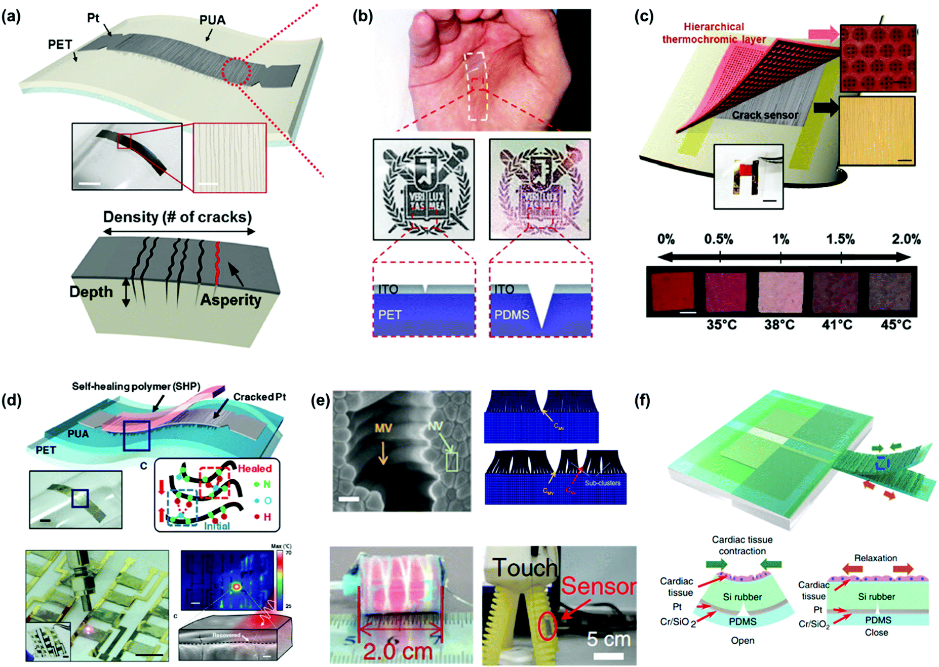 | ||
| Fig. 3 Various methods of producing mechanosensitive sensors. (a) Platinum thin film deposited over a PUA substrate acting as an ultra-sensitive strain sensor.33 (b) ITO crack-based transparent strain sensor.80 (c) Strain visualization using a hierarchical thermochromic layer with a crack-based sensor.81 (d) Heat induced healable crack sensor.82 (e) Stretchable sensor with high stability produced using vertically aligned nanowire networks.87 (f) Crack sensor measuring the contraction and relaxation of the cardiac tissue.90 | ||
In recent studies, additional functionality has been introduced by depositing a thermochromic layer on top of existing crack-based sensors,81 as depicted in Fig. 3c. Mechanical strain significantly decreases the number of electrical pathways in the structure, thereby leading to Joule heating of the thermochromic layer. This bilayer system provides a simple way of visualizing mechanical strain without external signal processing. It is also capable of carrying out respiration monitoring while attached to the ribs.
Since crack-based structures are mechanically unstable and have limited durability in practice due to fatigue crack growth during cyclical operations, a recent study (Fig. 3d) demonstrated the enhancement of the stability of the structure by coating it with a self-healing polymer.82 The polymer can be easily recovered at room temperature, allowing the sensitivity and operation to be consistent. Local healing is possible using a pointed infrared (IR) source, which can be leveraged for managing narrow sensory arrays.
As well as metal film-based sensors, a hierarchical cracking structure can be used to achieve both sensitivity and a broad sensing range.83–85 Wang et al. transferred CNTs onto PDMS to use as a stretchable sensing element, and pre-stretched to form hierarchical cracking networks.86 This sensor has high gauge factor (87) at 40% strain, which is also capable of measuring pulse signals on the wrist.
The studies described above relied on structures with horizontal percolation networks of metal particles or nanowires. Other recent work has demonstrated that vertical nanowire networks can provide a viable way of obtaining highly sensitive and stretchable structures while maintaining stability87 (Fig. 3e). The initial crack occurs between the nanowire clusters, with subsequent cracking occurring between individual nanowires. This two-step cracking enables high stretchability (130% strain) and a high gauge factor (>100). This type of structure can, therefore, be used as a sensing element in soft actuators and grippers.
As well as the nano-cracks generated mainly from the material, large micro-scale cracks can also be used in highly sensitive sensors. Reduced graphene oxide (RGO) sheets can be transferred onto PDMS by electrostatic coating, and the subsequent processes of steam-etching, dip-coating, and chemical vapor reduction can be used to fabricate precise sensor patterns.88 Micro-cracks enable the capture of various electrophysiological signals. Another study also utilized micro-cracks in CNT grids.89 CNTs were filled in the micro-meshed PDMS by a doctor-blading process and the micro-cracks were generated under strain of 5%. Sensors were attached imperceptibly to the skin (the transparency of the sensors was 87%) and were able to detect movements due to minute skin deformations and pulse signals.
As shown in Fig. 3f, Kim et al. developed a biosensing platform using a crack-based sensor.90 They showed higher measurement stability on culture media and suppression of performance degradation due to fatigue fracture by encapsulating it in PDMS. A platinum (Pt) layer deposited on top of the PDMS created cracks as the cardiac tissue contracted and relaxed. The system successfully measured cardiac contractility for a period of up to 26 days (>5 million heartbeats).
4.2 Other functional sensors
In order to sense environmental stimuli besides mechanical deformation, researchers have worked on various applications of detecting light91,92 and chemicals93,94 using crack structures. Hossain et al. demonstrated transparent and flexible photodetectors by random crack networks91 (Fig. 4a). They used an acrylic resin as a sacrificial layer and template: the resin spontaneously cracked and formed a random network while drying. After metal deposition, the lower silicon layer was then patterned using metal-assisted chemical etching. Finally, random silicon nanowire crack networks with an average width of 1 μm were generated. The silicon layer had excellent transparency (95%) at a wavelength of 550 nm. The detectivity was found to be 9 × 10¹¹ Jones, which is comparable to that of commercial Si-based non-transparent photodetectors (4 × 10¹² Jones).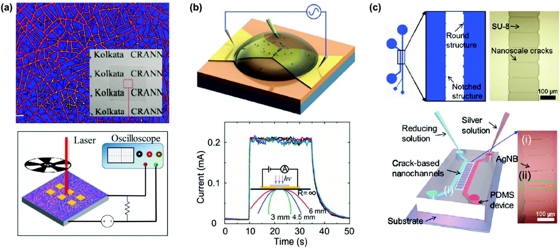 | ||
| Fig. 4 Applications of crack-based photo-and chemical detectors. (a) Transparent and flexible photodetector produced by a random crack network.91 (b) Ultraviolet sensor fabricated by swelling-induced cracks.92 (c) Use of crack-assisted microchannels for detecting chemicals.94 | ||
In another study,92 a nano crack gap was used to measure UV light (Fig. 4b). The researchers developed an efficient large-area fabrication method using swelling of the substrate. The metal layer was fabricated and patterned into a bow–tie structure using conventional lithography methods on an epoxy substrate. The structure was then immersed in ethanol, and the solvent permeated the necking area causing stretching of the lower substrate. Owing to the structure of the electrode, the stress was concentrated at the necking area and formed a nano-gap. ZnO nanoparticles were used as the sensor material between the nano-gaps; these were assembled using dielectrophoretic (DEP) assembly. The responsivity and EQE values (2.2 × 10⁷ A W−1 and 7.5 × 10⁹ %, respectively) exceeded those of existing semiconductor photodetectors. The sensor was also capable of making measurements while bent with a curvature of 3–6 mm.
Although the use of nanowires for chemical sensing has advantages because of their high sensitivity, their fabrication includes time- and labor-intensive aligning and patterning procedures. Therefore, researchers have developed simple methods of forming silver nano-belts using crack-assisted microchannels.94 As shown in Fig. 4c, first, notched SU-8 films and crack nano-patterns are made. PUA is then used to replicate the mold, and, finally, the PDMS nano-channels are produced by soft lithography. By injecting the silver and reducing solution, silver nano-belts are synthesized in the nano-channels. Nano-channels are then transferred between the metal electrodes and measure H2O2.
5. Other applications
In addition to functional devices, there are various other potential applications of controlled cracking, which are described below.5.1 Further electronic applications of crack lithography
Crack lithography is a widely used application of controlled cracking. Recently, crack lithography has attracted a lot of attention as it is possible to use this method to manufacture wide cracks by manipulating various parameters such as the type of material, the structure, or the initial stress. Various functional applications, including organic field-effect transistors (OFETs),95 molecular devices,96 terahertz antennas,97 and photovoltaic cells,98 have been developed in this way.X. Wang produced cracks with widths of 70–600 nm on PDMS by oxidizing the structure and then stretching it using notches. The structure was then used as a transfer printing stamp and gold electrodes with narrow gaps were constructed for use as the OFET channels.95 Similarly, in other recent research, double-layer graphene and Al2O3 films were deposited sequentially onto polyimide (PI) film.97 When tensile stress was applied to the structure, ordered cracks were generated in the Al2O3 film and the upper graphene layer, whereas, in the cracked region, the lower graphene layer was exposed. Using subsequent processing such as etching or metal deposition, these structures could be used to form various other structures such as graphene nano-slits, graphene–metallic nano-rods, metallic nano-rods, and metallic nano-slots. They could also be used to produce terahertz antennas, as shown in Fig. 5a.
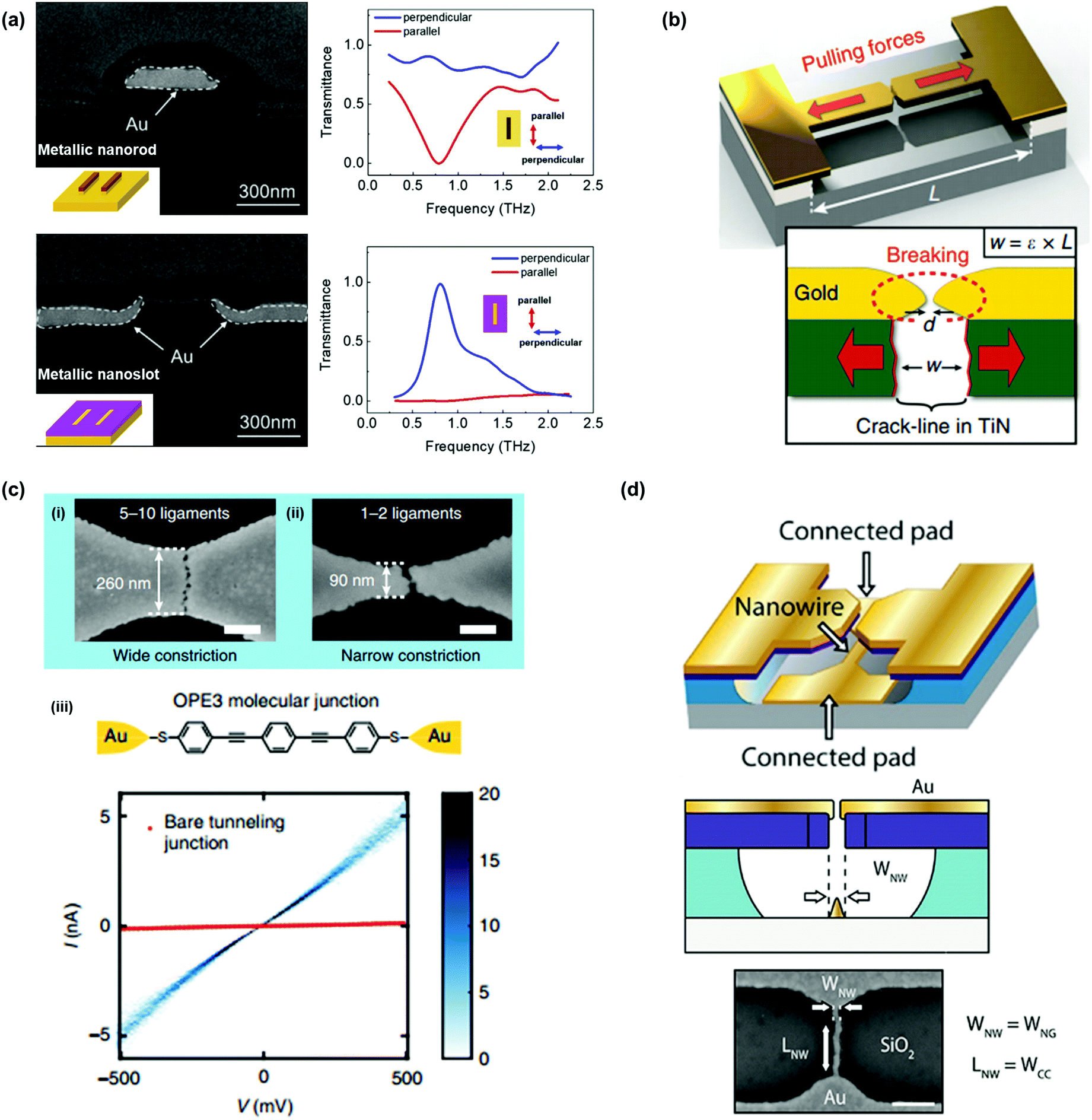 | ||
| Fig. 5 Further applications of crack lithography in electronics. (a) Using crack-induced lithography to fabricate terahertz antenna.97 (b) Using a release-etching technique to form a nano-gap in gold. (c) Generated nanogaps and a fabricated molecular device.96 (d) Using a nano-gap structure as a shadow mask to form a single nanowire.102 | ||
Thermal stress also can be used for generating nano-scale crack gaps with widths of about 150–300 nm. In addition, G. Purohit et al. used thermal stress to directly produce cracking in gold film, which is often used as the material for electrodes. In this study, notched Ti/Au/SiO2 structures were produced on a glass substrate, and cracks were induced by heating the structure to 300–500 °C.99
In order to narrow the crack spacing in the nano-gap channels, V. Dubois et al. introduced a release-etching technique for forming nano-gaps in various materials. In this process, a brittle thin film of TiN which has residual stress was deposited onto a sacrificial layer (Al2O3 or a-Si). After etching the sacrificial layer, the stress in the bridge was released, and the crack junction could be produced. Since TiN is conducting and the junction was at the sub-10 nm scale, this technique has a lot of potential for use in molecular electronics.100,101 In later research, these authors also produced a nano-gap in a ductile gold film using a similar method known as the crack-defined break junction.96 In this study, they used a-Si as the sacrificial layer and also deposited a gold electrode on to the TiN layer. The brittle TiN was deposited on to sacrificial a-Si coated substrates. The thin gold film was then deposited, and the layers were patterned to form notched bridges. After etching of the amorphous silicon layer, the tensile stress in the TiN cantilever induced cracks resulting in retraction in opposite directions. Then, the gold layer that had been deposited onto the TiN layer sequentially necked and produced ligaments, and formed the cracks that defined the break junction (Fig. 5b). The break junction that formed showed tunneling effects, and the conductance increased significantly when dithiol-terminated oligo (phenylene ethynylene) (OPE3) was deposited at the junction to form molecular devices (Fig. 5c).96 This structure can also be used as a shadow mask in the manufacture of single nanowire devices. After the crack structure had been produced and the metals (Au and Pd) deposited by PVD, the resulting single nanowire structure had a width of 10–20 nm and a length of 250–400 nm (Fig. 5d).102
In contrast, S. Oh et al. used a notch structure to selectively form cracks to isolate PV cells and release the residual stress in the GaAs epitaxial layer that appeared during cooling from the growth temperature of GaAs (700 °C) to room temperature. The self-isolated PV cell structure had a higher efficiency than other devices since the cracks were localized within the notch patterns in order to isolate the cells.98
5.2 Crack gap as a template or as microfluidic channels
In another approach, researchers have used cracks for patterning, or for manipulating the properties of various materials. For example, X. Zhu et al. fabricated cracks on PDMS that had been chemically modified not to be resistant to protein adsorption.103 Since the cracks were not resistant to protein adsorption, the proteins could be selectively grown. These proteins were also known to have reversible spreading and retraction characteristics as the channel changes by stretching, or by the release of PDMS. Similarly, in another study, 2D materials such as graphene or MoS2 were transferred onto oxidized and pre-stretched PDMS to manipulate the strain confinement effect.104 After release, crumpled 2D structures were localized within the cracked regions. In other research, attempts have been made to modulate the microfluidic properties of elastomer surfaces by mechanical stretching. A crack/fold hybrid structure was generated by mimicking the epidermis of desert lizards by stretching pre-patterned PDMS to form a layer of skin (Fig. 6a).105 In this case, an open crack was first filled with water; the water then spread through a semi-closed channel. In addition, if mechanical stretching was applied to this, the semi-closed fold channel opened up, and the water moved toward the crack channel (Fig. 6b). In addition to mechanical stretching of cracks, cracks generated by swelling of SU-8 can form narrow channels. T. Kim et al. made several studies of the production of SU-8-based cracks that involved crack initiating/termination structures and modification of the fracture stress using secondary exposure to UV light as explained in previous sections.49 As a result, cracks were selectively formed at pre-designed positions. This study was followed by several others that used PUA and PDMS, and, in this way, diffusion-based micro-/nano-fluidic devices were successfully produced (Fig. 6c and d).51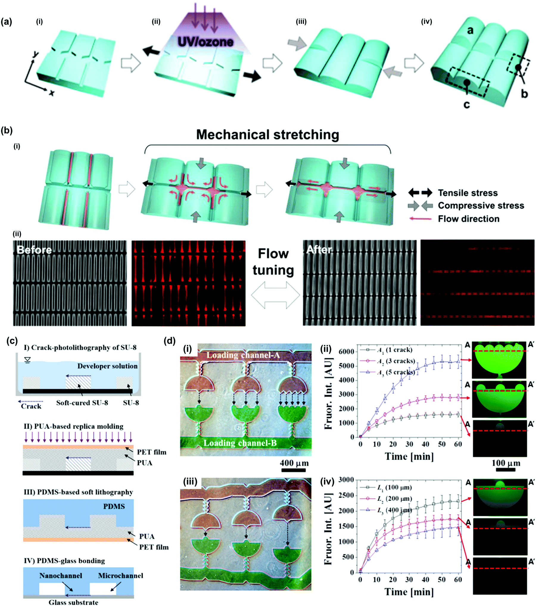 | ||
| Fig. 6 Cracked gaps as templates or microfluidic channels. (a) Fabrication process of Crack-fold hybrid structure.105 (b) Flow-tunability of desert lizard mimicking structures.105 (c) Fabrication process of crack-based micro-/nano-fluidic sensors.51 (d) Characteristics of micro-/nano-fluidic devices according to channel number and channel length.51 | ||
5.3 Three-dimensional approaches using controlled cracking
Recently, several studies about the production of 3D structures using crack control techniques have been published. S. Wooh et al. fabricated micro-pyramid structures by micro-patterning TiO2 nano-paste using PDMS molds that had been formed during the calcination process.106 It is also possible to fabricate mesoporous micro-pyramids or wire-shaped prisms using relatively large particles. Moreover, these structures have been demonstrated to have photocatalytic properties. In another approach by W. Li et al., 3D nano-structures were effectively replicated using a two-step process for curing PDMS.107 First, the PDMS, including the closed-loop master, was cured at a low temperature to form phase I (the low-modulus phase); the master was then removed to produce a crack gap. After the second, high-temperature curing stage, the crack was sealed. In this state, the replica material was filled and hardened to produce the replica. After removing the replica, the previously made crack was opened and the replica was successfully produced (Fig. 7a).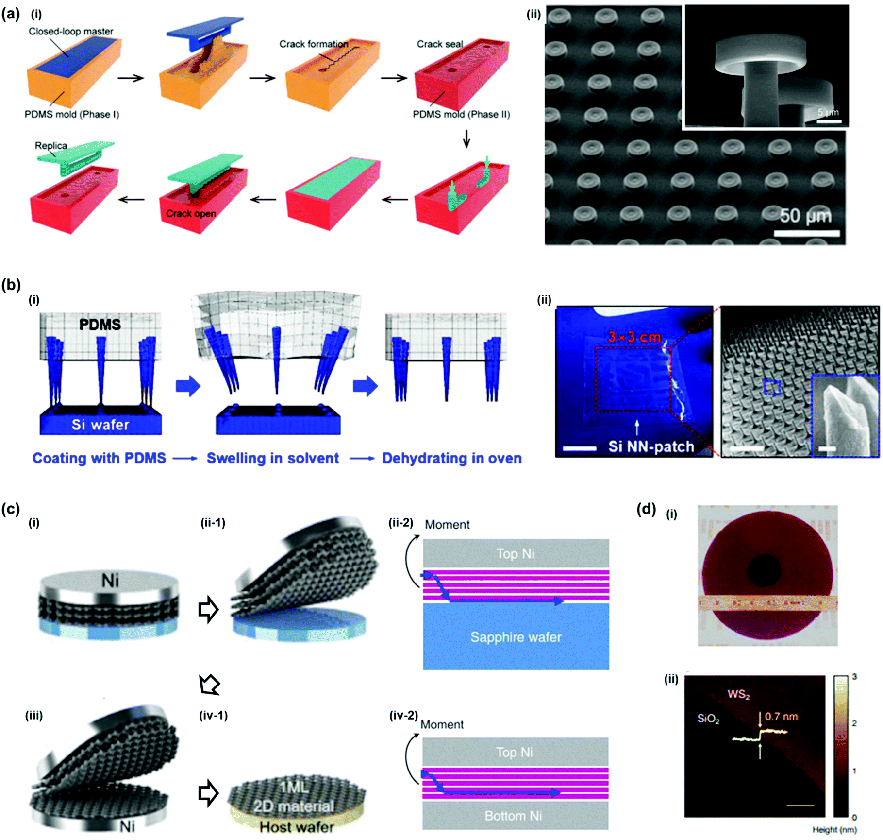 | ||
| Fig. 7 Three-dimensional approaches using controlled cracking. (a) Hierarchical structure fabrication processes and the magnified structures using a crack assisted molding process.107 (b) Nanoneedle fabrication processes, fabricated nanopatch and magnified structures.108 (c) Manipulation process for monolayer 2D materials showing lateral crack propagation direction.109 (d) Wafer-scale transferred 2D material composed of a monolayer.109 | ||
In order to produce a 3D nanoneedle array on elastomer substrates, H. Kim et al. used a swelling-induced cracking process.108 In this process, silicon pillar arrays were fabricated by conventional lithography and a deep reactive ion etching process. Next, the passivation layer was removed and etched by potassium hydroxide solution to reduce the overall size of the pillar. Following this, silicon nanoneedle arrays with tapered undercuts were formed on a silicon wafer with the silicon nanoneedles partially embedded in the PDMS. After this partial embedding, the entire structures were immersed in a solvent to swell the PDMS. The expansion of the PDMS induced crack generation at the localized undercuts of the silicon nanoneedles; the nanoneedles could then be successfully transferred to the PDMS substrate (Fig. 7b). The nanoneedle patches had many advantages such as mechanical flexibility, cell and tissue compatibility, and transparency. This enabled highly efficient nano-injection of biomolecules at the same time as observations were carried out.
It should be noted that the direction of crack propagation in the research that has been described was lateral whereas in other cases it is vertical. The application of lateral crack propagation has attracted much attention. For example, J. Shim et al. controlled the crack propagation between 2D materials and substrate materials by considering the interfacial toughness (Γ) and energy release rate: this was carried out to enable the precise handling of wafer-scale 2D materials.109 The so-called layer-resolved splitting (LRS) process can be applied to 2D materials such as hexagonal boron nitride (h-BN), tungsten disulfide (WS2), tungsten diselenide (WSe2), molybdenum disulfide (MoS2), and molybdenum diselenide (MoSe2). This process is based on differences in the interfacial toughness (Γ) between the materials. Since Γ between 2D materials and Ni (Γ2D–Ni) is higher than that between the layers in 2D materials (Γ2D–2D), a 600 nm thick Ni layer can be an effective adhesive for 2D materials. Moreover, the empirically deduced value of Γ between 2D materials and the sapphire substrate (Γ2D–sapphire) is very low and, thus, the whole 2D-material stack can be easily separated since the crack propagates through the 2D material and the sapphire substrate, which has the lowest interfacial toughness. After exfoliation from the sapphire substrate, the lower Ni layer is deposited to split the monolayer 2D materials. Then, during the peeling of the Ni/2D material stack from the lower Ni layer, the cracking propagates between the upper Ni/multilayer 2D materials and the monolayer 2D material/lower Ni since Γ2D–Ni > Γ2D–2D (Fig. 7c). Using this technique, the researchers successfully transferred large-scale monolayer 2D materials onto the host wafer (Fig. 7d). They demonstrated the uniformity of the WS2 monolayer by measuring the intensity of the photoluminescence (PL), which is significantly higher in the case of the monolayer.
M. Ito et al. also applied lateral cracking to produce structural color pigments; this is a similar method to the one that produces environmental stress cracking in plastics.110 In the case of environmental stress cracking, it is known that the size and shape of liquid molecules and also the Hansen solubility parameters affect the cracking behavior.111,112 However, these researchers mainly focused on the manipulation of internal stress by the cross-linking of polymers based on standing waves. An optical standing wave is formed when monochromatic plane waves interact with reflective surfaces. Using these standing waves, the polymers were laterally and periodically cross-linked in the presence of the photo-initiator. When polymers are cross-linked, residual stresses exist across the non-cross-linked layers. After the exposure to weak solvents, fractures propagate laterally through the non-cross-linked layers while forming microfiber structures. The layered structures exhibit structural color, the color being determined by the wavelength of the monochromatic plane waves.
6. Conclusions and perspectives
In this article, we have summarized recent research into the fabrication methods used for controlled cracking. In addition, we have reviewed the recent progress made in various functional applications that use controlled cracking as an alternative patterning tool.Previously, cracking was a phenomenon to be avoided due to its uncontrollable and random character. Therefore, at an earlier stage (about two decades ago) of cracking research, studies of cracking phenomena were mainly focused on the manipulation of cracking in various materials and analyses of the related mechanisms. However, it has since been demonstrated that crack phenomena have great potential for use as alternative patterning tools as they can allow faster production than conventional lithography-based methods and possess unique nano-gap features. In applications of transparent conductors, controlled cracking can be used as a patterning template that is compatible with large areas. It thus enables the fabrication of large nano-scale random metal networks. In other applications, the unique nano-scale structure of crack patterns can used as an alternative nano-fabrication technique for producing nano-gaps. This has many advantages in relation to the production of mechanical sensors and molecular devices.
Research into applications of controlled cracking started in the mid-2010s and much has been published subsequently. It is interesting to note that there are many studies from which one influential application has emerged. For example, after B. Han et al. first developed a transparent conductor using controlled crack patterning, numerous other research papers followed. Similarly, various studies of mechano-sensitive and functional sensors that use controlled cracking have developed from the mechano-sensitive sensors of D. Kang et al.'s research. Recent applications using controlled cracking in novel approaches such as silicon nanoneedle fabrication, micro/nano-scale hierarchical architecture fabrication, and very high-quality wafer-scale 2D-material handling methods are also expected to receive much attention from many researchers in the future.
In conclusion, recent advances in controlled cracking techniques are yielding new technological developments. Such developments will lead to continued progress in the use of the technique as an alternative patterning tool to the lithography method and lead to a paradigm shift toward precise, rapid, and large-area patterning. Since the cracking method can also be applied to various non-rigid, non-flat, flexible, and stretchable surfaces, it will also have an impact on soft electronics due to its outstanding advantages in relation to precision human–machine interaction devices and soft robotic control systems. Advances in the field of controlled cracking are also expected to provide new approaches in the development of wearable electronics, bio-compatible electronics, and soft robotics.
Conflicts of interest
There are no conflicts to declare.Acknowledgements
This work is supported by the National Research Foundation of Korea (NRF) Grant funded through the Basic Science Research Program (2017R1A2B3005706, NRF-2016R1A5A1938472). S. Hong was supported by an NRF grant funded through the Basic Science Research Program (NRF-2020R1C1C1013503). J. Yeo was supported by the NRF grant funded by the Korea government (NRF-2018R1A6A1A06024970, NRF-2019R1A2C1090510).References
- A. A. Griffith, Philos. Trans. R. Soc. London, 1921, 221, 163–198 CrossRef
.
- A. J. Pons and A. Karma, Nature, 2010, 464, 85–89 CrossRef CAS PubMed
- S. Massl, W. Thomma, J. Keckes and R. Pippan, Acta Mater., 2009, 57, 1768–1776 CrossRef CAS
- Y. Hayakawa, Phys. Rev. E: Stat. Phys., Plasmas, Fluids, Relat. Interdiscip. Top., 1994, 49, R1804–R1807 CrossRef PubMed
- V. Teixeira, Vacuum, 2002, 64, 393–399 CrossRef CAS
- J. Ma and G. Jing, Phys. Rev. E: Stat., Nonlinear, Soft Matter Phys., 2012, 86, 061406 CrossRef PubMed
- H. Lama, M. G. Basavaraj and D. K. Satapathy, Phys. Rev. Mater., 2018, 2, 085602 CrossRef CAS
- K. H. Nam, I. H. Park and S. H. Ko, Nature, 2012, 485, 221–224 CrossRef CAS PubMed
- Q. Zhao, J. Shao, H. Tian, X. Li, C. Wang and J. Liu, Sens. Actuators, B, 2018, 270, 475–481 CrossRef CAS
- H. H. Yu, M. Y. He and J. W. Hutchinson, Acta Mater., 2001, 49, 93–107 Search PubMed
- T. Sumigawa, T. Shishido, T. Murakami and T. Kitamura, J. Mater. Sci. Eng. A, 2010, 527, 4796–4803 CrossRef
- K. Kishimoto, Y. Yan, T. Sumigawa and T. Kitamura, Eng. Fract. Mech., 2012, 96, 72–81 CrossRef
- S. Y. Choi, M. Mamak, N. Coombs, N. Chopra and G. A. Ozin, Adv. Funct. Mater., 2004, 14, 335–344 Search PubMed
- Y. Xu, X. Zhu and S. Yang, ACS Nano, 2009, 3, 3251–3259 CrossRef CAS PubMed
- B. Hatton, L. Mishchenko, S. Davis, K. H. Sandhage and J. Aizenberg, Proc. Natl. Acad. Sci. U. S. A., 2010, 107, 10354 CrossRef CAS PubMed
- J. Lee, S. Chung, H. Song, S. Kim and Y. Hong, J. Phys. D: Appl. Phys., 2013, 46, 105305 CrossRef
- Q. Zhang, Y. Tang, M. Hajfathalian, C. Chen, K. T. Turner, D. A. Dikin, G. Lin and J. Yin, ACS Appl. Mater. Interfaces, 2017, 9, 44938–44947 CrossRef CAS PubMed
- A. Yuse and M. Sano, Nature, 1993, 362, 329–331 CrossRef CAS PubMed
- C. Allain and L. Limat, Phys. Rev. Lett., 1995, 74, 2981 CrossRef CAS PubMed
- J. Marthelot, B. Roman, J. Bico, J. Teisseire, D. Dalmas and F. Melo, Phys. Rev. Lett., 2014, 113, 085502 Search PubMed
- R. Seghir and S. Arscott, Sci. Rep., 2015, 5, 14787 Search PubMed
- B. Zhang, J. Lei, D. Qi, Z. Liu, Y. Wang, G. Xiao, J. Wu, W. Zhang, F. Huo and X. Chen, Adv. Funct. Mater., 2018, 28, 1801683 CrossRef
- L. Goehring, W. J. Clegg and A. F. Routh, Soft Matter, 2011, 7, 7984–7987 RSC
- H. Lama, M. G. Basavaraj and D. K. Satapathy, Soft Matter, 2017, 13, 5445–5452 RSC
- L. Xia, M. Zhang, Z. Yang, H. Cui, S. Yin, S. Hu and C. Du, Appl. Phys. Lett., 2014, 104, 073104 CrossRef
- G. Agarwal, H. Gao, M. Amirthalingam and M. Hermans, Metals, 2018, 8, 673 CrossRef
- C. Ishiyama, T. Sakuma, M. Shimojo and Y. Higo, J. Polym. Sci., Part B: Polym. Phys., 2002, 40, 1–9 CrossRef CAS
- Y. D. Suh, J. Yeo, H. Lee, S. Hong, J. Kwon, K. Kim and S. H. Ko, Sci. Rep., 2015, 5, 17292 CrossRef CAS PubMed
- R. G. Elliman, M. Spooner, T. D. M. Dall, T. H. Kim and N. H. Fletcher, Philos. Mag., 2007, 87, 4893–4906 CrossRef CAS
- M. R. Cho, J. H. Jung, M. K. Seo, S. U. Cho, Y. D. Kim, J. H. Lee, Y. S. Kim, P. Kim, J. Hone, J. Ihm and Y. D. Park, Sci. Rep., 2017, 7, 43400 Search PubMed
- D. P. H. Hasselman, J. Am. Ceram. Soc., 1969, 52, 600–604 CrossRef CAS
- K. Kokini and Y. R. Takeuchi, J. Mater. Sci. Eng. A, 1994, 189, 301–309 CrossRef
- B. Park, J. Kim, D. Kang, C. Jeong, K. S. Kim, J. U. Kim, P. J. Yoo and T. I. Kim, Adv. Mater., 2016, 28, 8130–8137 CrossRef CAS PubMed
- R. Gupta, K. D. M. Rao, K. Srivastava, A. Kumar, S. Kiruthika and G. U. Kulkarni, ACS Appl. Mater. Interfaces, 2014, 6, 13688–13696 Search PubMed
- S. Kiruthika, K. D. M. Rao, A. Kumar, R. Gupta and G. U. Kulkarni, Mater. Res. Express, 2014, 1, 026301 CrossRef
- J. M. Lagarón, J. M. Pastor and B. J. Kip, Polymer, 1999, 40, 1629–1636 CrossRef
- J. Arnold, J. Mater. Sci., 1998, 33, 5193–5204 CrossRef CAS
- M. Shanahan and J. Schultz, J. Polym. Sci., Polym. Phys. Ed., 1978, 16, 803–812 CrossRef CAS
-
E. Lucas, L. Ferreira and C. Khalil, Polymers Applications in Petroleum Production, in Encyclopedia of Polymer Science and Technology, ed. H. Mark, John Wiley & Sons, Inc., 2015, pp. 1–50 Search PubMed
- A. Yuse and M. Sano, Phys. D, 1997, 108, 365–378 CrossRef CAS
- O. Dalstein, E. Gkaniatsou, C. Sicard, O. Sel, H. Perrot, C. Serre, C. Boissière and M. Faustini, Angew. Chem., Int. Ed., 2017, 56, 14011–14015 CrossRef CAS
- B. C. Kim, C. Moraes, J. Huang, T. Matsuoka, M. D. Thouless and S. Takayama, Small, 2014, 10, 4020–4029 CrossRef CAS PubMed
- K. Fujimoto and T. Shioya, JSME Int. J., Ser. A, 2005, 48, 178–182 Search PubMed
- S. Yoneyama, K. Sakaue, H. Kikuta and M. Takashi, Exp. Mech., 2008, 48, 367–374 CrossRef
- L. Náhlík, K. Štegnerová and P. Hutař, Theor. Appl. Fract. Mech., 2018, 93, 247–262 CrossRef
- K. R. Phillips, C. T. Zhang, T. Yang, T. Kay, C. Gao, S. Brandt, L. Liu, H. Yang, Y. Li, J. Aizenberg and L. Li, Adv. Funct. Mater., 2019, 1908242 CrossRef
- E. Lee, T. Kim, H. Suh, M. Kim, P. V. Pikhitsa, S. Han, J. S. Koh and D. Kang, Sensors, 2018, 18, 2872 CrossRef PubMed
- B. E. Alaca, H. Sehitoglu and T. Saif, Appl. Phys. Lett., 2004, 84, 4669–4671 CrossRef CAS
- M. Kim, D. Ha and T. Kim, Nat. Commun., 2015, 6, 6247 Search PubMed
- K. H. Nam, Y. D. Suh, J. Yeo and D. Woo, Sci. Rep., 2016, 6, 18892 Search PubMed
- M. Kim and T. Kim, Anal. Chem., 2015, 87, 11215–11223 CrossRef CAS PubMed
- J. Gao, Z. Xian, G. Zhou, J.-M. Liu and K. Kempa, Adv. Funct. Mater., 2018, 28, 1705023 CrossRef
- Q. Peng, S. Li, B. Han, Q. Rong, X. Lu, Q. Wang, M. Zeng, G. Zhou, J.-M. Liu, K. Kempa and J. Gao, Adv. Mater. Technol., 2016, 1, 1600095 Search PubMed
- S. Kiruthika, R. Gupta, K. D. M. Rao, S. Chakraborty, N. Padmavathy and G. U. Kulkarni, J. Mater. Chem. C, 2014, 2, 2089–2094 RSC
- Y. Han, J. Lin, Y. Liu, H. Fu, Y. Ma, P. Jin and J. Tan, Sci. Rep., 2016, 6, 25601 CrossRef CAS PubMed
- K. D. M. Rao, R. Gupta and G. U. Kulkarni, Adv. Mater. Interfaces, 2014, 1, 1400090 CrossRef
- Y. D. Suh, S. Hong, J. Lee, H. Lee, S. Jung, J. Kwon, H. Moon, P. Won, J. Shin, J. Yeo and S. H. Ko, RSC Adv., 2016, 6, 57434–57440 RSC
- J. Jung, H. Cho, S. H. Choi, D. Kim, J. Kwon, J. Shin, S. Hong, H. Kim, Y. Yoon, J. Lee, D. Lee, Y. D. Suh and S. H. Ko, ACS Appl. Mater. Interfaces, 2019, 11, 15773–15780 CrossRef CAS PubMed
- B. Han, Q. Peng, R. Li, Q. Rong, Y. Ding, E. M. Akinoglu, X. Wu, X. Wang, X. Lu, Q. Wang, G. Zhou, J.-M. Liu, Z. Ren, M. Giersig, A. Herczynski, K. Kempa and J. Gao, Nat. Commun., 2016, 7, 12825 Search PubMed
- B. Han, K. Pei, Y. Huang, X. Zhang, Q. Rong, Q. Lin, Y. Guo, T. Sun, C. Guo, D. Carnahan, M. Giersig, Y. Wang, J. Gao, Z. Ren and K. Kempa, Adv. Mater., 2014, 26, 873–877 CrossRef CAS PubMed
- Y.-g. Kim, Y. J. Tak, S. P. Park, H. J. Kim and H. J. Kim, Nanomaterials, 2017, 7, 214 CrossRef PubMed
- Y. D. Suh, J. Kwon, J. Lee, H. Lee, S. Jeong, D. Kim, H. Cho, J. Yeo and S. H. Ko, Adv. Electron. Mater., 2016, 2, 1600277 CrossRef
- C. Yang, J. M. Merlo, J. Kong, Z. Xian, B. Han, G. Zhou, J. Gao, M. J. Burns, K. Kempa and M. J. Naughton, Phys. Status Solidi A, 2018, 215, 1700504 CrossRef
- Z. Xian, B. Han, S. Li, C. Yang, S. Wu, X. Lu, X. Gao, M. Zeng, Q. Wang, P. Bai, M. J. Naughton, G. Zhou, J.-M. Liu, K. Kempa and J. Gao, Adv. Mater. Technol., 2017, 2, 1700061 CrossRef
- Y. Han, Y. Liu, L. Han, J. Lin and P. Jin, Carbon, 2017, 115, 34–42 CrossRef CAS
- S. Liu, C. Chen, D. Zhang, G. Dong, D. Zheng, Y. Jiang, G. Zhou, J.-M. Liu, K. Kempa and J. Gao, Nanoscale Res. Lett., 2019, 14, 127 Search PubMed
- G. Dong, S. Liu, M. Pan, G. Zhou, J.-M. Liu, K. Kempa and J. Gao, Adv. Mater. Technol., 2019, 4, 1900056 CrossRef CAS
- D. Kang, P. V. Pikhitsa, Y. W. Choi, C. Lee, S. S. Shin, L. Piao, B. Park, K. Y. Suh, T. I. Kim and M. Choi, Nature, 2014, 516, 222–226 CrossRef CAS PubMed
- H. Jung, C. Park, H. Lee, S. Hong, H. Kim and S. J. Cho, Sensors, 2019, 19, 2834 CrossRef CAS PubMed
- J. Ye, T. Yang, Y. Zhang and L. Lin, Adv. Mater. Interfaces, 2018, 5, 1800616 CrossRef
- T. Yang, X. Li, X. Jiang, S. Lin, J. Lao, J. Shi, Z. Zhen, Z. Li and H. Zhu, Mater. Horiz., 2016, 3, 248–255 RSC
- Z. Han, L. Liu, J. Zhang, Q. Han, K. Wang, H. Song, Z. Wang, Z. Jiao, S. Niu and L. Ren, Nanoscale, 2018, 10, 15178–15186 RSC
- M. Amjadi, M. Turan, C. P. Clementson and M. Sitti, ACS Appl. Mater. Interfaces, 2016, 8, 5618–5626 CrossRef CAS PubMed
- S. K. Hong, S. Yang, S. J. Cho, H. Jeon and G. Lim, Sensors, 2018, 18, 1171 CrossRef PubMed
- Q. Li, K. Wang, Y. Gao, J. Tan, R. Wu and F. Xuan, Appl. Phys. Lett., 2018, 112, 263501 Search PubMed
- T. Lee, Y. W. Choi, G. Lee, S. M. Kim, D. Kang and M. Choi, RSC Adv., 2017, 7, 34810–34815 RSC
- T. Kim, T. Lee, G. Lee, Y. Choi, S. Kim, D. Kang and M. Choi, Appl. Sci., 2018, 8, 367 CrossRef
- Y. W. Choi, D. Kang, P. V. Pikhitsa, T. Lee, S. M. Kim, G. Lee, D. Tahk and M. Choi, Sci. Rep., 2017, 7, 40116 CrossRef CAS PubMed
- C.-J. Lee, K. H. Park, C. J. Han, M. S. Oh, B. You, Y.-S. Kim and J.-W. Kim, Sci. Rep., 2017, 7, 1–8 CrossRef
- T. Lee, Y. W. Choi, G. Lee, P. V. Pikhitsa, D. Kang, S. M. Kim and M. Choi, J. Mater. Chem. C, 2016, 4, 9947–9953 RSC
- B. Park, J. U. Kim, J. Kim, D. Tahk, C. Jeong, J. Ok, J. H. Shin, D. Kang and T. I. Kim, Adv. Funct. Mater., 2019, 29, 1903360 CrossRef
- B. Park, S. Lee, H. Choi, J. U. Kim, H. Hong, C. Jeong, D. Kang and T. I. Kim, Nanoscale, 2018, 10, 4354–4360 Search PubMed
- S. Chen, Y. Wei, S. Wei, Y. Lin and L. Liu, ACS Appl. Mater. Interfaces, 2016, 8, 25563–25570 CrossRef CAS PubMed
- D. H. Ho, R. Song, Q. Sun, W. H. Park, S. Y. Kim, C. Pang, D. H. Kim, S. Y. Kim, J. Lee and J. H. Cho, ACS Appl. Mater. Interfaces, 2017, 9, 44678–44686 CrossRef CAS PubMed
- H. Jeon, S. K. Hong, M. S. Kim, S. J. Cho and G. Lim, ACS Appl. Mater. Interfaces, 2017, 9, 41712–41721 CrossRef CAS PubMed
- S. Wang, P. Xiao, Y. Liang, J. Zhang, Y. Huang, S. Wu, S.-W. Kuo and T. Chen, J. Mater. Chem. C, 2018, 6, 5140–5147 RSC
- W. Miao, Y. Yao, Z. Zhang, C. Ma, S. Li, J. Tang, H. Liu, Z. Liu, D. Wang, M. A. Camburn, J. C. Fang, R. Hao, X. Fang, S. Zheng, N. Hu and X. Wang, Nat. Commun., 2019, 10, 3862 CrossRef PubMed
- Y. J. Yun, J. Ju, J. H. Lee, S. H. Moon, S. J. Park, Y. H. Kim, W. G. Hong, D. H. Ha, H. Jang and G. H. Lee, Adv. Funct. Mater., 2017, 27, 1701513 CrossRef
- B. Nie, X. Li, J. Shao, X. Li, H. Tian, D. Wang, Q. Zhang and B. Lu, ACS Appl. Mater. Interfaces, 2017, 9, 40681–40689 CrossRef CAS PubMed
- D.-S. Kim, Y. W. Choi, A. Shanmugasundaram, Y.-J. Jeong, J. Park, N.-E. Oyunbaatar, E.-S. Kim, M. Choi and D.-W. Lee, Nat. Commun., 2020, 11, 1–13 CrossRef PubMed
- M. Hossain, G. S. Kumar, S. N. Barimar Prabhava, E. D. Sheerin, D. McCloskey, S. Acharya, K. D. M. Rao and J. J. Boland, ACS Nano, 2018, 12, 4727–4735 Search PubMed
- Q. Zhao, W. Wang, J. Shao, X. Li, H. Tian, L. Liu, X. Mei, Y. Ding and B. Lu, Adv. Mater., 2016, 28, 6337–6344 CrossRef CAS PubMed
- J. Lee, W. Shim, E. Lee, J. S. Noh and W. Lee, Angew. Chem., Int. Ed., 2011, 50, 5301–5305 CrossRef CAS PubMed
- D. J. Kim, D. Ha, Q. Zhou, A. K. Thokchom, J. W. Lim, J. Lee, J. G. Park and T. Kim, Nanoscale, 2017, 9, 9622–9630 RSC
- X. Wang, T. Fu and Z. Wang, Nanotechnology, 2018, 29, 145301 CrossRef PubMed
- V. Dubois, S. N. Raja, P. Gehring, S. Caneva, H. S. J. van der Zant, F. Niklaus and G. Stemme, Nat. Commun., 2018, 9, 3433 CrossRef
- S. Won, H.-J. Jung, D. Kim, S.-H. Lee, D. Van Lam, H.-D. Kim, K.-S. Kim, S.-M. Lee, M. Seo, D.-S. Kim, H.-J. Lee and J.-H. Kim, Carbon, 2020, 158, 505–512 Search PubMed
- S. Oh, D. H. Jun, K. W. Shin, I. Choi, S. H. Jung, J. Choi, W. Park, Y. Park and E. Yoon, IEEE J. Photovolt., 2016, 6, 1031–1035 Search PubMed
- G. Purohit, Deepak and M. Katiyar, RSC Adv., 2018, 8, 4928–4936 Search PubMed
- V. Dubois, F. Niklaus and G. Stemme, Adv. Mater., 2016, 28, 2178–2182 CrossRef CAS PubMed
- V. Dubois, F. Niklaus and G. Stemme, Microsyst. Nanoeng., 2017, 3, 17042 CrossRef PubMed
- A. Enrico, V. Dubois, F. Niklaus and G. Stemme, ACS Appl. Mater. Interfaces, 2019, 11, 8217–8226 CrossRef CAS PubMed
- X. Zhu, K. L. Mills, P. R. Peters, J. H. Bahng, E. H. Liu, J. Shim, K. Naruse, M. E. Csete, M. D. Thouless and S. Takayama, Nat. Mater., 2005, 4, 403–406 CrossRef CAS
- J. Leem, Y. Lee, M. C. Wang, J. M. Kim, J. Mun, M. F. Haque, S.-W. Kang and S. Nam, 2D Mater., 2019, 6, 044001 CrossRef CAS
- J. Cha, H. Shin and P. Kim, ACS Appl. Mater. Interfaces, 2016, 8, 28418–28423 CrossRef CAS
- S. Wooh, S. Lee, Y. Lee, J. H. Ryu, W. B. Lee, H. Yoon and K. Char, ACS Nano, 2016, 10, 9259–9266 Search PubMed
- W. Li, M. Yu, J. Sun, K. Mochizuki, S. Chen, H. Zheng, J. Li, S. Yao, H. Wu, B. S. Ong, S. Kawata, Z. Wang and K. Ren, Proc. Natl. Acad. Sci. U. S. A., 2019, 116, 23909 CrossRef CAS PubMed
- H. Kim, H. Jang, B. Kim, M. K. Kim, D. S. Wie, H. S. Lee, D. R. Kim and C. H. Lee, Sci. Adv., 2018, 4, eaau6972 CrossRef CAS PubMed
- J. Shim, S.-H. Bae, W. Kong, D. Lee, K. Qiao, D. Nezich, Y. J. Park, R. Zhao, S. Sundaram, X. Li, H. Yeon, C. Choi, H. Kum, R. Yue, G. Zhou, Y. Ou, K. Lee, J. Moodera, X. Zhao, J.-H. Ahn, C. Hinkle, A. Ougazzaden and J. Kim, Science, 2018, 362, 665 CrossRef CAS PubMed
- M. M. Ito, A. H. Gibbons, D. Qin, D. Yamamoto, H. Jiang, D. Yamaguchi, K. Tanaka and E. Sivaniah, Nature, 2019, 570, 363–367 CrossRef CAS PubMed
- A. Ward, X. Lu, Y. Huang and N. Brown, Polymer, 1991, 32, 2172–2178 CrossRef CAS
- C. M. Hansen and L. Just, Ind. Eng. Chem. Res., 2001, 40, 21–25 CrossRef CAS
Footnote |
| † J. Jung and K. K. Kim equally contributed to this work. |
| This journal is © The Royal Society of Chemistry 2020 |