
 Open Access Article
 This Open Access Article is licensed under a Creative Commons Attribution-Non Commercial 3.0 Unported Licence
Hydrogen gas sensing using aluminum doped ZnO metasurfaces†
Sharmistha
Chatterjee
 ab,
Evgeniy
Shkondin
c,
Osamu
Takayama
d,
Adam
Fisher
b,
Arwa
Fraiwan
e,
Umut A.
Gurkan
efgh,
Andrei V.
Lavrinenko
d and
Giuseppe
Strangi
*ab
ab,
Evgeniy
Shkondin
c,
Osamu
Takayama
d,
Adam
Fisher
b,
Arwa
Fraiwan
e,
Umut A.
Gurkan
efgh,
Andrei V.
Lavrinenko
d and
Giuseppe
Strangi
*ab
aCNR-NANOTEC Istituto di Nanotecnologia, Department of Physics, University of Calabria, 87036 Rende, Italy
bDepartment of Physics, Case Western Reserve University, 10600 Euclid Avenue, Cleveland, OH 44106, USA. E-mail: gxs284@case.edu; Tel: +1 216 368 6918
cDTU Nanolab – National Center for Micro- and Nanofabrication, Technical University of Denmark, Ørsteds Plads 347, DK-2800 Kgs, Lyngby, Denmark
dDTU Fotonik – Department of Photonics Engineering, Technical University of Denmark, Ørsteds Plads 343, DK-2800 Kgs, Lyngby, Denmark
eCase Biomanufacturing and Microfabrication Laboratory, Mechanical and Aerospace Engineering Department, Case Western Reserve University, Cleveland, Ohio 44106, USA
fBiomedical Engineering Department, Case Western Reserve University, Cleveland, Ohio 44106, USA
gDepartment of Orthopedics, Case Western Reserve University, Cleveland, Ohio 44106, USA
hAdvanced Platform Technology Center, Louis Stokes Cleveland Veterans Affairs Medical Center, Cleveland, Ohio 44106, USA
First published on 18th June 2020
Abstract
Hydrogen (H2) sensing is crucial in a wide variety of areas, such as industrial, environmental, energy and biomedical applications. However, engineering a practical, reliable, fast, sensitive and cost-effective hydrogen sensor is a persistent challenge. Here we demonstrate hydrogen sensing using aluminum-doped zinc oxide (AZO) metasurfaces based on optical read-out. The proposed sensing system consists of highly ordered AZO nanotubes (hollow pillars) standing on a SiO2 layer deposited on a Si wafer. Upon exposure to hydrogen gas, the AZO nanotube system shows a wavelength shift in the minimum reflectance by ∼13 nm within 10 minutes for a hydrogen concentration of 4%. These AZO nanotubes can also sense the presence of a low concentration (0.7%) of hydrogen gas within 10 minutes. Their rapid response time even for a low concentration, the possibility of large sensing area fabrication with good precision, and high sensitivity at room temperature make these highly ordered nanotube structures a promising miniaturized H2 gas sensor.
Introduction
Hydrogen (H2) gas is a highly combustible diatomic gas with low ignition energy. Therefore, when hydrogen gas leaks into the external air, it may spontaneously ignite the environment and cause an explosion, which is extremely hazardous. Hydrogen gas, within a concentration range of 4 to 75% is considered combustible.1 As H2 is a tasteless non-toxic gas, it is hard to detect by human senses. Apart from the danger of explosion, hydrogen poses a number of threats, such as asphyxiation in its pure, oxygen-free form2 and frostbite associated with very cold liquid cryogenic hydrogen.3 Therefore, for safety considerations, the detection of low hydrogen concentrations within a very short time is crucial in industries where it is considered an obvious component or a byproduct.Chromatography and mass spectrometry are widely used for large scale industrial H2 gas sensing. However, these techniques are not suitable for use in miniaturized systems such as in the food industry and medical applications where the detection of ultra-low concentrations of exhaled hydrogen has to be performed over a smaller area.4–6 Until now, many groups reported some nanophotonic and nanoplasmonic system-based optical hydrogen sensors which work by controlling light at the sub-wavelength scale using metallic components.5,7,8 However, in most cases, the metallic systems are characterized by high optical losses, while metal hydrides have low loss but are relatively more selective. Moreover, the sensing systems fabricated by lithography have low throughput and are inclined to imperfections and thus may be unsuitable for optical detection of hydrogen gas.9,10
As losses are inherent to plasmonic substances, alternative materials with lower optical losses are more suitable for sensing platforms. Zinc oxide (ZnO)-based nanostructures,11 as a dielectric material, have been studied extensively as highly sensitive, selective and efficient gas sensors for the detection of various hazardous and toxic gases such as NO, NO2,12,13 ammonia (NH3),14 methane (CH4),14,15 acetone,16 ethanol,17–20 humidity,21 CO,14,22–24 volatile organic compounds (VOCs),25 and hydrogen.15,26–38 According to the literature, ZnO holds promise in the development of technologies based on resistive-type gas sensors for electrical readouts. However, the high operating temperature, slow response time and poor selectivity and stability limit its extensive applications in the field of dissolved gas monitoring. In the electrical detection method the presence of H2 gas is detected by monitoring the change of the resistivity of ZnO structures. On the contrary, optical detection is desirable not only because of the easy readout but also for the stringent safety conditions.
Here we experimentally demonstrate hydrogen sensing using metasurfaces made of aluminum-doped zinc oxide (AZO) nanotubes (hollow pillars). We conduct a comparative study on the gas sensing properties of the solid AZO pillars. The high aspect ratio AZO pillars and nanotubes are fabricated using a combination of advanced reactive ion etching and atomic layer deposition (ALD) techniques.39 The solid AZO pillars do not respond to H2 gas of concentration 0.7–4% at room temperature and pressure even after a long exposure time. On the other hand, the AZO nanotubes show a wavelength shift of ∼13 nm upon exposure to H2 gas of 4% concentration at ambient temperature, and a simultaneous decrease in the reflectance intensity of ∼0.4% is also detected within 10 minutes. This structure can even sense the presence of low concentrations (0.7%) of H2 gas within the same response time. In order to understand the sensing mechanism of the AZO metasurfaces, numerical simulations are performed to simulate the experimental behavior of the AZO nanotubes exposed to H2 gas. In particular, the following paragraphs describe the design and the nanofabrication process of the metasurfaces along with finite element method (FEM) based Comsol simulations to understand the peculiar aspects of the interaction of light waves on the metasurfaces. Then the sensing experiments are described starting with the engineering of microfluidic gas flow chambers.
Experimental section
Fabrication of AZO nanotubes
Two types of samples were fabricated: AZO solid pillars and nanotube structures on a Si substrate with a thermally grown 200 nm silica layer (see Fig. 1). The external diameter, thickness, and height of the AZO nanotubes are 300 nm, 20 nm, and 2 μm, respectively, and a pitch of 400 nm is maintained over a 1 × 1 cm2 area. On the other hand, the diameter and height of the AZO solid pillars are 300 nm and 2 μm, respectively, and a pitch of 400 nm is also maintained here over the same area. For both types of structures, air acts as the host material. Elemental analysis by transmission electron microscopy (TEM) and other characterization methods as well as extended details on fabrication of AZO pillars and nanotubes can be found elsewhere.39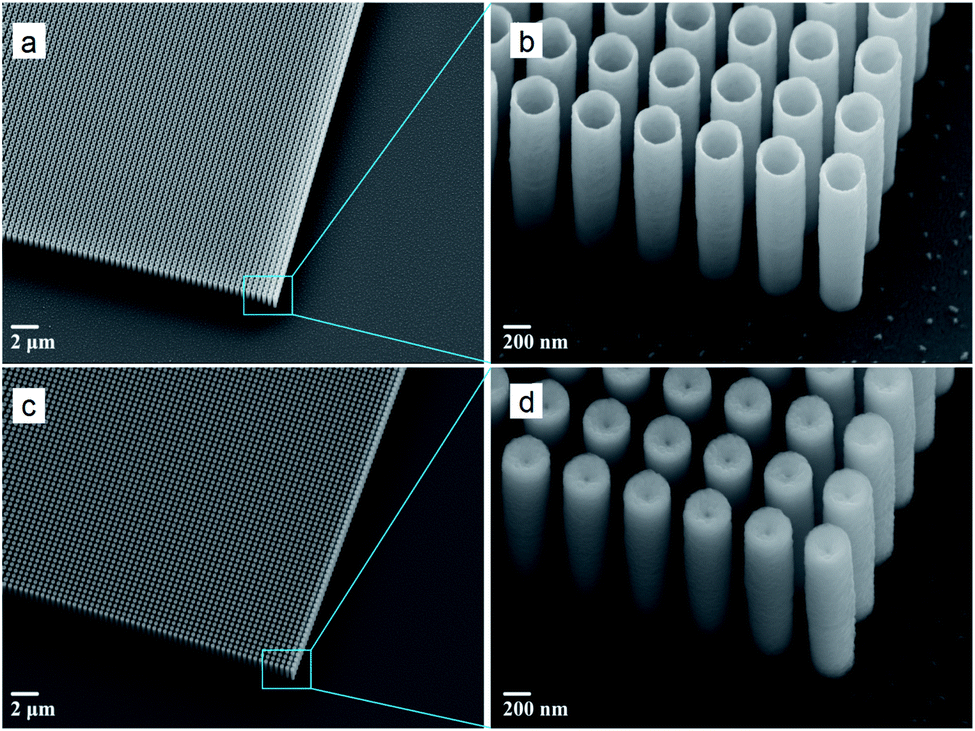 | ||
| Fig. 1 Scanning electron microscope (SEM) images of the fabricated AZO (a, b) nanotubes and (c, d) pillar structures with a pitch of 400 nm, diameter of 300 nm, and height of 2 μm. The wall thickness of nanotubes is approximately 20 nm. | ||
Deep-UV lithography was used to define grating patterns on SOI wafers that are composed of a 2 μm thick Si layer deposited on a thermally grown 200 nm silica layer on standard silicon 〈100〉 wafers. DRIE was implemented with a standard Bosch process40 in order to fabricate a Si template with 2 μm-deep air hole arrays. Afterwards, the processed structures were cleaned in N2/O2 plasma in order to remove remaining photoresist and other organic contaminants. Then, the silicon templates were coated with AZO (using trimethylaluminum, diethylzinc, and water as precursors) by means of atomic layer deposition (ALD), partially filling the holes with a 20 nm thick AZO layer to create AZO tubes. Note that AZO pillars were fabricated by filling the air holes entirely. ALD is based on self-limiting, sequential surface chemical reactions which allow conformal deposition on complex structures with thickness control.41 For the final step, the AZO filling needs to be isolated, and for this purpose, the samples were subjected to Ar+ sputtering for removal of the top AZO layer and exposure of the silicon template. Afterwards, the silicon template in between cavities coated with AZO was removed using SF6 plasma in a conventional isotropic reactive ion etching process without interference with a functional ALD material, resulting in the formation of AZO pillars and tubes as shown in Fig. 1. A more detailed description of the fabrication method for different structures, such as AZO trenches,42–44 TiN trenches,45 dielectric trenches,46 and coaxial tubes,47 can be found elsewhere. The optical properties of AZO films fabricated by ALD were measured using a spectroscopic ellipsometer in the wavelength range of interest.39,42
Fabrication of the microfluidic channel
The microfluidic channel is made up of a poly(methyl methacrylate) (PMMA) plastic window which is surrounded by micromachined inlets and outlets. Along with this a double-sided adhesive film is attached which defines the outlines and thickness of the microfluidic channel. The diameter of inlets and outlets of the PMMA top is 0.61 mm and a separation distance of 12.4 mm is maintained here. The PMMA top is fabricated by laser micromachining using a VersaLASER system (Universal Laser Systems). A double-sided adhesive film (iTapestore, 100 μm in height) is laser micro-machined to have the same precise size of the PMMA top and is placed within the 14 × 2 mm micro-channel. Here the adhesive film is attached to the PMMA top to include the inlet and outlet within the outline of the channel. To connect the gas sources with the microfluidic channel, fluorinated ethylene propylene (FEP) tubing (Cole-Parmer) is used. All the tubings and their connections between gas sources and channels are fastened using 5 min epoxy (Devcon). For clarity a picture of our sensor (Fig. S1) is given in the ESI.†Ellipsometric reflection measurements for gas sensing
A high-resolution variable angle spectroscopic ellipsometer (SE) (J. A. Woollam Co., Inc., V-VASE) is used to experimentally measure all types of angular reflection data as illustrated in Fig. 2a. The low-power spectroscopic ellipsometer has high precision and it is non-destructive and thus preferable for the optical characterization of nanostructures and gas sensing. In order to characterize the performance of our gas sensing system, AZO nanotubes are exposed to H2 gas of different concentrations. The channel inlet is connected to a tank of nitrogen mixed with a 4% volume concentration of H2 and to another of pure nitrogen. The gas flow from both the tanks is controlled separately using two separate mass flow controllers (MFCs). By adjusting these MFCs, we could control the hydrogen concentration (between 0 and 4%) introduced into the sample as illustrated in Fig. 2b. After adjusting all these parameters the sensor was placed on the variable angle ellipsometer to measure the reflectivity R (λ, ϕ) at different angles of incidence, ϕ, in the wavelength range of λ = 300–1500 nm. The maximum resolution of this ellipsometer is 0.03 nm but for our measurements 1 nm resolution is maintained throughout the experiments. Note that for all the optical H2 gas sensing measurements in this work we considered TE-polarized incident light because it has a much stronger wavelength dependence compared to TM-polarized light and thus is more advantageous for precise measurements of wavelength shift for different concentrations of H2 gas (see Fig. S2 in the ESI†). The polarization dependence stems from the tube structure. In the case of TE-polarized light (the electric field oscillation along the x-direction) where the field penetrates the 20 nm thick AZO tube walls and interacts with the tubes, the change of the AZO tubes' permittivity due to the presence of H2 results in a more optical response than with TM-polarized light with fewer field components penetrating AZO tubes. During the gas sensing experiment, because of the PMMA window on top of the channel, the incident beam splits into two reflected beams at the interfaces of Air–PMMA window and PMMA window–microfluidic channel, causing Fabry–Perót fringes in the reflection spectra. In order to minimize the effect and keep the associated error at a minimum, the particular suitable incident angle for the sensing set-up needs to be optimized. Here the measurement angle is kept below or equal to ϕ = 45°. Moreover, the iris of the ellipsometer detector helps to block the additional reflected beam during the sensing measurement, an unavoidable source of experimental error which originates from the insertion of the microfluidic channel. After fixing the measurement angle to see the response of the AZO sensing system for H2 gas of a particular concentration, the reflectance is continuously measured over a wavelength range (selected based on the minima of reflectance) for 90 minutes maintaining a constant time interval between each measurement.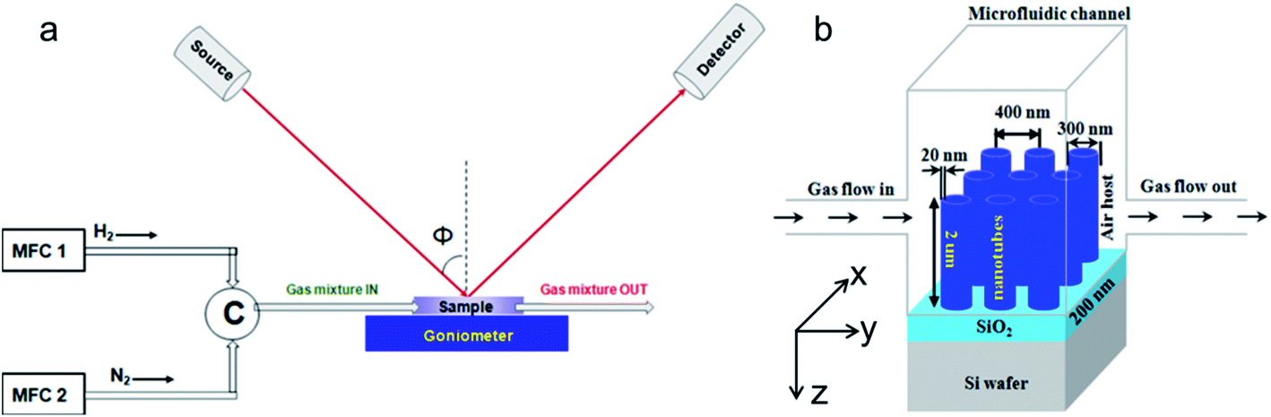 | ||
| Fig. 2 (a) Schematic diagram of the experimental set-up. (b) Schematic diagram of the AZO nanotube sensing system. | ||
Finite element method (FEM) simulation
Finite Element Method (FEM) simulation is carried out to describe the interaction between light and AZO nanotubes with a 300 nm external diameter, 20 nm wall thickness, 2 μm height and 400 nm periodicity in a square lattice arrangement (and also with AZO solid nanopillars of 300 nm diameter, 2 μm height and 400 nm pitch with the same type of lattice arrangement). In order to map out the electric field pattern in the nanotube structures interacting with light we used the Radio Frequency (RF) module of the FEM based COMSOL 5.4 software package. During this theoretical study, all the specifications about the size, shape, and substrates of AZO nanotubes are obtained from the SEM results. Moreover, the COMSOL material library is used to obtain the optical properties of air as the surrounding medium, the SiO2 layer, and the Si substrate. The wavelength dependent complex permittivity with both real and imaginary parts of AZO is taken from the experimental data obtained from spectroscopic ellipsometry measurements and proper fitting.39 At first for this study a unit cell composed of a single AZO nanotube (or nanopillar) on top of a SiO2 layer on a Si wafer is considered as depicted in Fig. 3b and c. The dimensions of the unit cell in both the x- and y-direction are 400 nm which is the pitch of both AZO nanostructures used for gas sensing experiments. Here linearly polarized plane waves are used as the excitation source. Periodic ports (z-direction) are used to launch the TE polarized plane waves at an angle of 45° which is identical to the gas sensing experimental framework. Periodic boundary conditions are used in both the x- and y-directions which allow us to build an infinite array of nanostructures (AZO nanotubes/nanopillars) by periodically replicating the same defined unit cell. Physics controlled free triangular and tetrahedral meshes (depending on different layers) are used for these analyses to calculate the electromagnetic power loss density (W m−3) and the electric field enhancement with a suitable and variable mesh size where the lowest mesh size is maintianed at 1.6 nm.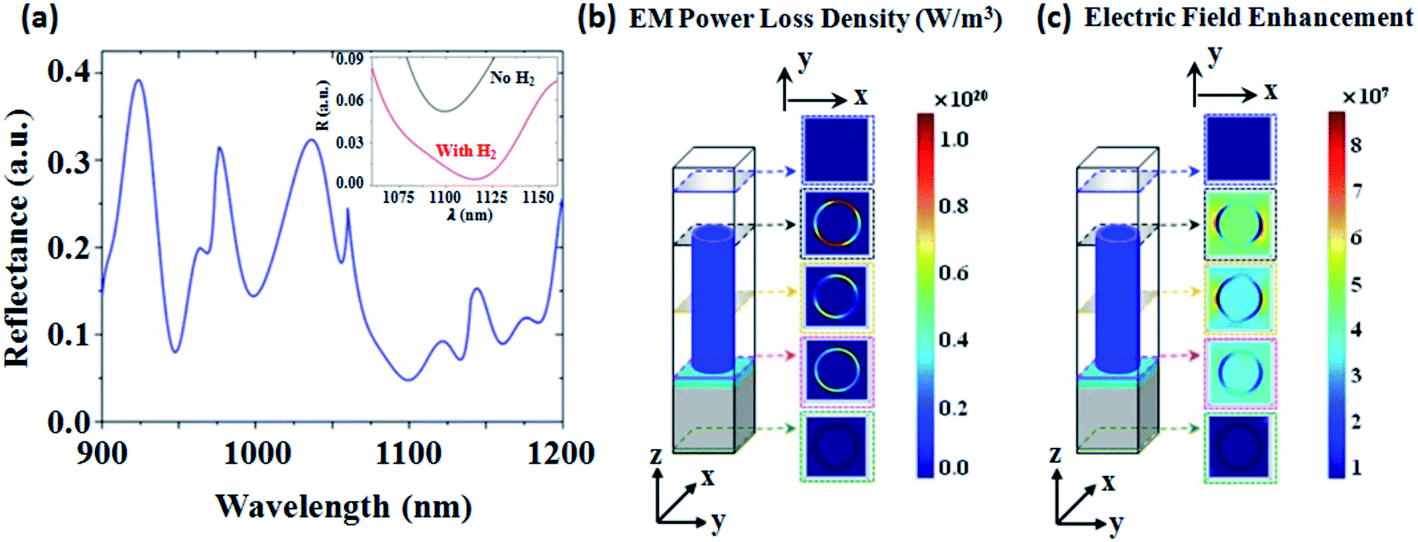 | ||
| Fig. 3 Simulation results. (a) Reflection spectra of an array system composed of the AZO nanotube unit cell as shown in panel (b) and (c). (b) The electromagnetic power loss density (W m−3) and (c) electric field profile at 1100 nm wavelength in the AZO nanotube unit cell. The inset figure shown in panel (a) depicts the change in the 1100 nm mode of the reflectance spectra after intercalation of H2 gas. Here simulation for the linearly polarized incident plane wave (TE-polarized light with the electric field parallel to the surface of tubes along the x-axis) is investigated. The periodicity, thickness of walls, and height of tubes are 400 nm, 20 nm, and 2 μm, respectively. The incident angle is ϕ = 45. | ||
Results and discussion
Finite element method (FEM) simulation
Fig. 3a shows the simulated reflection from AZO nanotubes. The incident angle is taken as ϕ = 45° similar to the experimental case. Here a 400 nm periodicity, 20 nm thick tube wall, and 2 μm height are considered. The direction of the electric field of the incident light is taken along the x-axis (TE-polarized incident light). The inset in Fig. 3a shows the numerically calculated shift of the 1100 nm mode in the reflectance spectra after H2 gas injection.During simulation the refractive index of hydrogen is assumed to be 1.00014.48 The wavelength shift in this case is 17 nm and the change in intensity of the reflectance minimum mode is 0.048 (see Fig. S3 in the ESI† for more details). The electromagnetic power loss density (W m−3) associated with the AZO nanotube unit cell for plane incident waves is shown in Fig. 3b at 1100 nm, which is one of the reflection minimum modes in the theoretical reflectance spectra of AZO nanotubes shown in Fig. 3a. Here, it is clear that the optical loss is concentrated mostly within the AZO nanotubes. The light absorption in the AZO tube layer suggests that the AZO tubes' absorption properties can be significantly modified by the environmental conditions. The simulated electric field profile of the same unit cell at the wavelength of 1100 nm is shown in Fig. 3c and depicts the high electric field enhancement near the surface of AZO nanotubes, useful for the detection of any changes of the AZO nanotubes' optical properties. Here it is worth mentioning that AZO solid nanopillars are seen to not respond to H2 gas both experimentally and theoretically. The computational gas sensing response is shown in Fig. S4† and the experimental response is given in Fig. S5.†
Hydrogen sensing by AZO nanotubes
We study the spectral shift, Δλ, for different hydrogen concentrations. Fig. 4a shows the response of the AZO nanotube system to 0.7% H2 gas at ϕ = 45° over a wavelength range of λ = 300–1500 nm. This plot shows that for a particular measurement angle the wavelength shift, Δλ, is larger for longer wavelengths, giving higher sensitivity. For example, for ϕ = 45°, the wavelength shift of the reflectance minima around λ = 900 nm is Δλ = 0 nm, while the reflectance minima at λ = 1126 nm shift by Δλ = 2.6 nm for 0.7% H2 gas. Depending on the angle of incidence for measurement, the sensitivity can also be tuned. More detailed information about the dependence of wavelength shift and sensitivity on the measurement angle variation is given in the ESI (Fig. S6†). We note that for longer wavelengths the fluctuation in reflectance increases due to Fabry–Perót interference originating from the PMMA window of the microfluidic channel, which can be observed in Fig. S7.† Taking these factors into account, here we focus on the reflection minima around a 1100 nm wavelength for hydrogen sensing. | ||
| Fig. 4 The response of AZO nanotubes in the presence of hydrogen gas. (a) The response of the AZO nanotube sensing system before and after intercalation of 0.7% H2 gas measured at an incident angle of ϕ = 45° over a wavelength range of λ = 300–1500 nm. Using this plot one can choose the suitable mode for H2 gas detection with higher sensitivity. (b) 0.7%, (c) 2%, and (d) 4% H2 gas sensing results. For all these measurements, the response time is 10 min. The wavelength shift, Δλ, for 0.7%, 2%, and 4% H2 gas is 2.6 nm, 5 nm and 13 nm, respectively. | ||
In Fig. 4b–d, the properly fitted H2 gas sensing response of the AZO nanotube array system is presented for concentrations of 0.7%, 2%, and 4%, respectively. For all these measurements the response time was 10 minutes. Here, the system shows a wavelength shift, Δλ, and reflectance intensity change, ΔI, even for the lowest concentration of 0.7% H2 gas. The wavelength shift is 2.6 nm for 0.7% H2 and the change in reflectance intensity is 0.2%. Similarly, the wavelength shift is 5 nm for 2% H2 and the change in reflectance intensity is nearly 0.3%. For 4% H2 gas the wavelength shift is 13 nm and the reflectance intensity change is 0.4%. In comparison to the theoretically calculated wavelength shift (17 nm) and the intensity change (0.0475) of the reflectance minimum mode, the experimental changes even for the case of 4% H2 gas are a little bit smaller. This is because of the consideration of ideal situations in the case of theoretical analysis.
When light activated-AZO nanotubes interact with atmospheric air, oxygen molecules get absorbed on the surface of the nanotubes which further extract electrons from the conduction band of the ZnO site. When a reducing gas like H2 intercalates into the system, these light-activated chemisorbed oxygen ions on the surface of AZO nanotubes interact with the reductive gas molecules, donate free electrons back to the conduction band of ZnO and produce water molecules.49 This local change in the polarizability and thus the surrounding refractive index contributes to the shift of reflection minima in the presence of H2 gas. Here it is worth mentioning that the metal doping in ZnO nanotubes increases the photo-generated free electron–hole pairs and, because of the resonant plasmonic effect, the light absorption capacity is enhanced which further results in more sites for the oxygen molecules on the surface of AZO nanotubes.49 The AZO nanotube-based metasurface as a Fabry–Perót cavity senses the presence and concentration of H2 gas by detecting the change in polarizability due to the chemical changes in the surrounding media.
If wavelength shift is considered the measurement parameter, the signal to noise ratio (S/N) becomes 16.7% which is equivalent to the wavelength shift/FWHM (Full Width at Half Maximum) of the mode. In order to characterize the sensitivity in terms of reflectance change, the figure of merit (FOM) is defined as FOM = R (AZOair)/R (AZOH2) × 100,8 where R (AZOair) is the reflectance of the sensor in N2 (which is equivalent to air media) without hydrogen and R (AZOH2) is the reflectance of the sensor in the presence of hydrogen gas. According to Fig. 4d for 4% H2 gas, the calculated FOM of our sensor is ∼104. Note that we also conducted reflectance measurements for AZO solid pillars in the presence of 4% H2 gas over 90 minutes. However, even after such a long time, there is no clear change observed in the reflectance minimum mode in terms of wavelength shift or reflectance intensity change for such gas sensing with the solid AZO pillars (see Fig. S5 in the ESI†). This indicates that the ultra thin wall thickness of AZO nanotubes and their hollowness play an important role in sensing due to their larger surface area to volume ratio relative to the solid pillars.50 Here it is worth mentioning that, for AZO nanotubes (hollow pillars), the surface area to volume ratio is nearly 13.2 times larger than that of the solid AZO pillars.
Fig. 5a and b display the wavelength shift and the intensity change in the reflectance minima of the AZO metasurface after exposure to H2 gas with different concentrations. Based on the measurement of the wavelength shift, here the limit of detection (LOD) is 0.2% H2 for 10 minutes of response time considering the fact that the maximum possible resolution of the used spectroscopic ellipsometer is 0.03 nm (see Fig. S8 in the ESI†). It is well-known that practical hydrogen sensors must be able to respond to hydrogen at concentrations approximately an order of magnitude lower than the explosive limit of H2 (4%).8,49 Previous work has demonstrated a Pd-based optical H2 gas sensor with a high FOM at room temperature.8 However, the response time was nearly 60 minutes, which can be an issue for safety in the industrial field. Our AZO nanotube array system could achieve this requirement in terms of a fast response time of 10 minutes at room temperature by means of safe optical measurement.
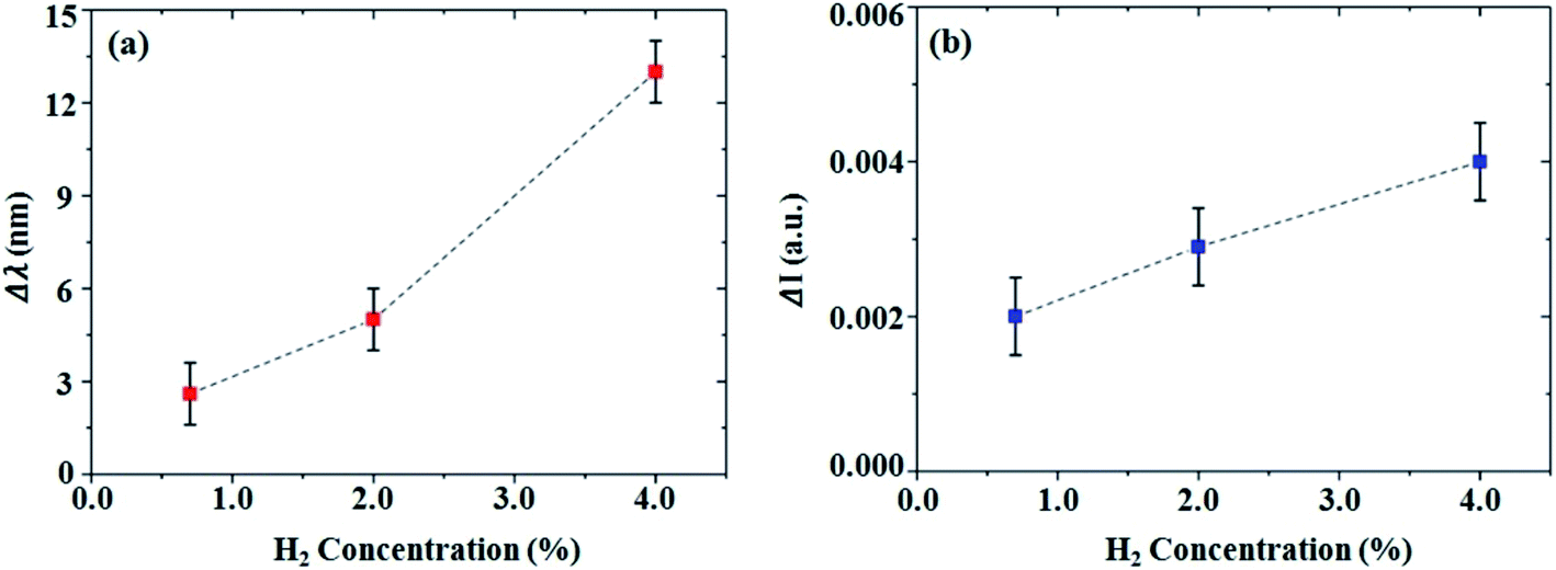 | ||
| Fig. 5 Variation of experimental (a) wavelength shift, Δλ, and (b) reflectance intensity change of reflection minima, ΔI, observed in the AZO nanotube sensing system in the presence of H2 gas of different concentrations (0.7%, 2%, and 4%). Here the dotted lines are for guidance to see how Δλ and ΔI change for different concentrations of H2 gas. | ||
The results of gas sensing response over time up to 90 minutes for 4% H2 gas are shown in Fig. 6a from which we can see the fast response nature of the AZO nanotube sensor. Here it can be seen that 10 minutes is sufficient to detect 4% H2 gas. This response time is also valid for 2% and 0.7% H2 gas. Fig. 6b shows the response of AZO nanotubes under different conditions. Here the ellipsometric responses of the AZO nanotube system with the PMMA channel in the absence of any gas as well as in the presence of pure N2 gas and 4% H2 gas are shown.
 | ||
| Fig. 6 (a) Response of the AZO nanotube sensing system over time in the presence of 4% H2 gas. It is very clear that 10 min is enough to detect the presence of 4% H2 gas. (b) The response of the AZO nanotube sensing system (with the PMMA channel) in the presence and absence of N2 gas where there is almost no variation in the mode. But a clear shift of the mode is observed in the presence of 4% H2 gas after 60 min. | ||
In this plot, we do not observe any wavelength shift in reflection after introducing pure N2 gas into the sensor (dashed red curve) compared to the reflectance when the sample is not exposed to any gas (black curve). In comparison, after introducing N2 mixed with 4% H2 (cyan curve), we observe a clear red shift in the reflection minimum, as well as a change in the reflection amplitude due to the intercalation of hydrogen atoms in the sensing system as expected. After H2 gas sensing measurements, to regain its primary reflectance position we stopped the H2 gas flow in the channel and introduced pure N2 to purge all the gases in the chamber so that the initial atmospheric conditions could be achieved. However, the reflectance of the sensing system did not go back to its primary position demonstrating the presence of hysteresis in the system. The experimental results regarding the hysteresis in the system are given in the ESI (see Fig. S9†). For this hysteresis related study all the experiments were carried out at room temperature only, and no special treatment, for example, applying external heat or pressure or any chemical treatment was performed. The absorption properties of the AZO nanotube sensing system remain unaffected in air for a long time demonstrating its stability.
Conclusion
In summary, we report the study of the H2 gas sensing properties of a metasurface made up of highly ordered high aspect ratio aluminium-doped zinc oxide (AZO) nanotubes designed to operate in the NIR range, around 1100 nm. While AZO solid pillars do not respond to H2 gas, AZO nanotubes show a wavelength shift as well as a significant decrease in the reflectance intensity after exposure to H2 gas. Here H2 gas sensing is observed at room temperature and pressure within a response time of 10 minutes. Therefore, the possibility of having a room-temperature H2 gas sensor, with all the advantages of low-response time, ability to detect low concentrations of H2 gas, a good figure of merit, and possibility of fabricating a large area sensor with high precision and reliability can make these metasurfaces the platform for very promising H2 gas sensors for industrial applications. Moreover, the sensitivity of nanotubes may be further enhanced by controlling the doping level of ZnO with aluminum. AZO metasurfaces hold promise for realizing room temperature gas sensors, which may enable monitoring hydrogen gas by color changes in the visible range.Author contributions
S. C. wrote the manuscript and conducted modeling and theoretical analysis of the structures. S. C. and A. F. performed optical characterization for hydrogen sensing. E. S. fabricated the samples. A. F. and U. A. G. built the microfluidic cell. O. T. and A. V. L. contributed to the discussions of the results and manuscript writing. G. S. conceived the idea and supervised the work. All authors have given approval to the final version of the manuscript.Conflicts of interest
The authors declare no competing financial interests.Acknowledgements
This work was supported by the Independent Research Fund Denmark, DFF Research Project 2 “PhotoHub” (8022-00387B), Villum Fonden “DarkSILD project” (11116), Direktor Ib Henriksens Fund, Denmark, and NSF Grant (Award Number 1904592) – Instrument Development: Multiplex Sensory Interfaces Between Photonic Nanostructures and Thin Film Ionic Liquids. The authors would like to acknowledge the support from the National Centre for Nano Fabrication and Characterization (DTU Nanolab).References
- N. R. Fong, P. Berini and R. N. Tait, Nanoscale, 2016, 8, 4284–4290 RSC.
- W. J. Brown, National Aeronautics and Space Administration, NASA, 1997 Search PubMed.
- E. Overview, Liquid Hydrogen MSDS (PDF), Praxair, Inc., 2004, 1985–1986 Search PubMed.
- J. R. Wilkins, G. E. Stoner and E. H. Boykin, Appl. Microbiol., 1974, 27, 949–952 CrossRef CAS PubMed.
- A. Tittl, P. Mai, R. Taubert, D. Dregely, N. Liu and H. Giessen, Nano Lett., 2011, 11, 4366 CrossRef CAS PubMed.
- C. Wadell, S. Syrenova and C. Langhammer, ACS Nano, 2014, 8, 11925–11940 CrossRef CAS PubMed.
- N. Liu, Nat. Mater., 2011, 10, 631–636 CrossRef CAS PubMed.
- M. ElKabbash, K. V. Sreekanth, Y. Alapan, M. Kim, J. Cole, A. Fraiwan, T. Letsou, Y. Li, C. Guo, R. M. Sankaran, U. A. Gurkan, M. Hinczewski and G. Strangi, ACS Photonics, 2019, 6, 1889–1894 CrossRef CAS.
- P. Ngene, T. Radeva, M. Slaman, R. J. Westerwaal, H. Schreuders and B. Dam, Adv. Funct. Mater., 2014, 24, 2374–2382 CrossRef CAS.
- Z. Li, S. Butun and K. Aydin, ACS Photonics, 2015, 2, 183–188 CrossRef CAS.
- V. S. Bhati, M. Hojamberdiev and M. Kumar, Energy Reports, 2020, 6, 46–62 CrossRef.
- M. W. Ahn, K. S. Park, J. H. Heo, J. G. Park, D. W. Kim, K. J. Choi, J. H. Lee and S. H. Hong, Appl. Phys. Lett., 2008, 93, 263103 CrossRef.
- R. Kumar, O. Al-Dossary, G. Kumar and A. Umar, Nano-Micro Lett., 2015, 7, 97–120 CrossRef PubMed.
- S. Ryong Ryu, S. D. Ram, H. D. Cho, D. J. Lee, T. Won Kang and Y. Woo, Nanoscale, 2015, 7, 11115–11122 RSC.
- O. Lupan, V. Postica, J. Grottrup, A. K. Mishra, N. H. De Leeuw, J. F. Carreira, J. Rodrigues, N. Ben Sedrine, M. R. Correia, T. Monteiro, V. Cretu, I. Tiginyanu, D. Smazna, Y. K. Mishra and R. Adelung, ACS Appl. Mater. Interfaces, 2017, 9, 4084–4099 CrossRef CAS PubMed.
- F. Morisot, C. Zuliani, J. Luque, Z. Ali, M. Mouis, V. H. Nguyen, D. Munoz-Rojas, O. Lourhzal, M. Texier, T. W. Cornelius and C. Ternon, Mater. Res. Express, 2019, 6, 084004 CrossRef CAS.
- Q. Wan, Q. H. Li, Y. J. Chen, T. H. Wang, X. L. He, J. P. Li and C. L. Lin, Appl. Phys. Lett., 2004, 84, 3654–3656 CrossRef CAS.
- T. J. Hsueh, S. J. Chang, C. L. Hsu, Y. R. Lin and I. C. Chen, Appl. Phys. Lett., 2007, 91, 053111 CrossRef.
- J. Y. Son, S. J. Lim, J. H. Cho, W. K. Seong and H. Kim, Appl. Phys. Lett., 2008, 93, 053109 CrossRef.
- C. Wang, Z.-G. Wang, R. Xi, L. Zhang, S.-H. Zhang and L.-J. Wang, Sens. Actuators, B, 2019, 292, 270–276 CrossRef CAS.
- R. Majithia, S. Ritter and K. E. Meissner, Anal. Chim. Acta, 2014, 812, 206–214 CrossRef CAS PubMed.
- A. Katoch, S.-W. Choi and S. S. Kim, Nanotechnology, 2014, 25, 455504 CrossRef PubMed.
- A. Paliwal, A. Sharma, M. Tomar and V. Gupta, Sens. Actuators, B, 2017, 250, 679–685 CrossRef CAS.
- J.-H. Kim, A. Mirzaei, H. Woo and S. Sub, Sens. Actuators, B, 2018, 267, 597–607 CrossRef CAS.
- S. Ozturk, A. Kosemen, Z. Alpaslan, N. Kilinc, Z. Z. Ozturk and M. Penza, Sens. Actuators, B, 2016, 222, 280–289 CrossRef CAS.
- T. C. Narayan, F. Hayee, A. Baldi, A. L. Koh, R. Sinclair and J. A. Dionne, Nat. Commun., 2017, 8, 14020 CrossRef CAS PubMed.
- T. F. Choo, N. U. Saidin and K. Y. Kok, R. Soc. Open Sci., 2018, 5, 172372 CrossRef PubMed.
- H. T. Wang, B. S. Kang, F. Ren, L. C. Tien, P. W. Sadik, D. P. Norton, S. J. Pearton and J. Lin, Appl. Phys. Lett., 2005, 86, 243503 CrossRef.
- S. N. Das, J. P. Kar, J. H. Choi, T. Lee, K. J. Moon and J. M. Myoung, J. Phys. Chem. C, 2010, 114, 1689–1693 CrossRef CAS.
- M. A. Lim, D. H. Kim, C. O. Park, Y. W. Lee, S. W. Han, Z. Li, R. S. Williams and I. Park, ACS Nano, 2012, 6, 598–608 CrossRef CAS PubMed.
- M. Kashif, M. E. Ali, S. M. Usman and U. Hashim, Ceram. Int., 2013, 39, 6461–6466 CrossRef CAS.
- S. Ranwa, P. K. Kulriya, V. K. Sahu, L. M. Kukreja and M. Kumar, Appl. Phys. Lett., 2014, 105, 213103 CrossRef.
- A. Katoch, S. W. Choi, H. Woo and S. Sub, J. Hazard. Mater., 2015, 286, 229–235 CrossRef CAS PubMed.
- M. Faisal, B. Alam, D.-T. Phan and G.-S. Chung, Mater. Lett., 2015, 156, 113–117 CrossRef.
- D. Kathiravan, B. R. Huang and A. Saravanan, ACS Appl. Mater. Interfaces, 2017, 9, 12064–12072 CrossRef CAS PubMed.
- M. Zhao, M. Hon, H. Chung and C. Wo, Sens. Actuators, B, 2017, 249, 624–631 CrossRef CAS.
- V. S. Bhati, S. Ranwa, S. Rajamani, K. Kumari, R. Raliya, P. Biswas and M. Kumar, ACS Appl. Mater. Interfaces, 2018, 10, 11116–11124 CrossRef CAS PubMed.
- J.-H. Kim, A. Mirzaei, H. Woo, P. Wu and S. Sub, Sens. Actuators, B, 2019, 293, 210–223 CrossRef CAS.
- E. Shkondin, O. Takayama, M. E. A. Panah, P. Liu, P. V. Larsen, M. D. Mar, F. Jensen and A. V. Lavrinenko, Opt. Mater. Express, 2017, 7, 1606–1627 CrossRef CAS.
- V. Lindroos, M. Tilli, A. Lehto, T. Motooka and T. Veijola, Handbook of silicon based MEMS materials and technologies, Micro & Nano Technologies Series, 2010 Search PubMed.
- S. George, Chem. Rev., 2010, 110, 111–131 CrossRef CAS PubMed.
- O. Takayama, E. Shkondin, A. Bogdanov, M. E. Aryaee Pahah, K. Golenitskii, P. A. Dmitriev, T. Repan, R. Malreanu, P. Belov, F. Jensen and A. V. Lavrinenko, ACS Photonics, 2017, 4, 2899–2907 CrossRef CAS.
- O. Takayama, P. Dmitriev, E. Shkondin, O. Yermakov, K. Golenitskii, F. Jensen, A. Bogdanov and A. V. Lavrinenko, Semiconductors, 2018, 52, 442–446 CrossRef CAS.
- E. Shkondin, T. Repan, M. E. A. Panah, A. V. Lavrinenko and O. Takayama, ACS Appl. Nano Mater., 2018, 1, 1212–1218 CrossRef CAS.
- E. Shkondin, T. Repan, O. Takayama and A. V. Lavrinenko, Opt. Mater. Express, 2017, 7, 4171–4182 CrossRef CAS.
- E. Shkondin, O. Takayama, J. M. Lindhard, P. V. Larsen, M. D. Mar, F. Jensen and A. V. Lavrinenko, J. Vac. Sci. Technol., A, 2016, 34, 031605 CrossRef.
- E. Shkondin, H. Alimadadi, O. Takayama, F. Jensen and A. V. Lavrinenko, J. Vac. Sci. Technol., A, 2020, 38, 013402 CrossRef.
- E. R. Peck and S. Huang, J. Opt. Soc. Am., 1977, 67, 1550 CrossRef CAS.
- J. R. Pitts, P. Liu, S. Lee, C. E. Tracy and A. Hopkins, Proceedings of the 2000 DOE Hydrogen Program Review, 2000, pp. 1–16 Search PubMed.
- A. Katoch, Z. U. Abideen, J.-H. Kim and S. S. Kim, Sens. Actuators, B, 2016, 232, 698–704 CrossRef CAS.
Footnote |
| † Electronic supplementary information (ESI) available. See DOI: 10.1039/d0na00289e |
| This journal is © The Royal Society of Chemistry 2020 |