
 Open Access Article
 This Open Access Article is licensed under a Creative Commons Attribution-Non Commercial 3.0 Unported Licence
Enhancement of organic solar cell performance by incorporating gold quantum dots (AuQDs) on a plasmonic grating†
Sopit
Phetsang
ab,
Supeera
Nootchanat
a,
Chutiparn
Lertvachirapaiboon
 a,
Ryousuke
Ishikawa‡
a,
Kazunari
Shinbo
a,
Keizo
Kato
a,
Pitchaya
Mungkornasawakul
b,
Kontad
Ounnunkad
*bc and
Akira
Baba
*a
a,
Ryousuke
Ishikawa‡
a,
Kazunari
Shinbo
a,
Keizo
Kato
a,
Pitchaya
Mungkornasawakul
b,
Kontad
Ounnunkad
*bc and
Akira
Baba
*a
aGraduate School of Science and Technology, Niigata University, 8050 Ikarashi-2-nocho, Nishi-ku, Niigata 950-2181, Japan. E-mail: ababa@eng.niigata-u.ac.jp
bDepartment of Chemistry and Center of Excellence for Innovation in Chemistry (PERCH-CIC), Faculty of Science, Chiang Mai University, Chiang Mai 50200, Thailand. E-mail: kontad.ounnunkad@cmu.ac.th
cCenter of Excellence for Innovation in Chemistry, Faculty of Science, Center of Excellence in Materials Science and Technology, Research Center on Chemistry for Development of Health Promoting Products from Northern Resources, Chiang Mai University, Chiang Mai 50200, Thailand
First published on 8th June 2020
Abstract
The incorporation of metallic nanoobjects into devices allows to increase light harvesting, which increases the device performance. In this study, we used a combination of gold quantum dots and grating-coupled surface plasmon resonance (GCSPR) to improve the performance of organic solar cells (OSCs) with a poly(3-hexylthiophene-2,5-diyl) (P3HT):[6,6]-phenyl C61 butyric acid methyl ester (PCBM) photoactive layer. Gold quantum dots with a green fluorescent color (green-AuQD) were loaded into a hole transport layer (HTL) aiming to harvest photons in the UV region and emit visible light into the neighboring photoactive layer. Meanwhile, plasmonic grating structures, which were created on the photoactive layer surfaces via the nanoimprinting technique, provided an enhancement effect through light scattering and GCSPR. Thus, an excellent enhancement of OSC efficiency with a significant increase in short circuit photocurrent (JSC) and power conversion efficiency (PCE) in comparison to that of the reference cell was achieved. The fabricated device provides a JSC value as high as 8.41 mA cm−2 (a 14.11% enhancement) and a PCE value of 3.91% (a 19.57% enhancement). The systematic study clearly reveals that the remarkable enhancement of OSC efficiency is achieved by incorporating both AuQD and plasmonic grating.
Introduction
Currently, the use of alternative energy sources has become more attractive owing to the increasing need for energy consumption with low carbon dioxide emission. Sunlight is a renewable free energy that can be harvested and converted to electricity by solar cells. Different from conventional silicon solar cells, organic solar cells (OSCs) offer unique advantages including low cost, simple fabrication, flexibility, and low weight.1–4 Although OSCs have a good photoelectric conversion efficiency, the diffusion length of the photogenerated excitons in the photoactive layer is relatively short (typically 10 nm). This limits the thickness of the photoactive layer to the typical range of 100–200 nm, which results in the insufficient optical absorption with a consequent low photocurrent generation.3,5–7 An increase in the photoactive layer thickness may improve the light absorption but induces the recombination of free charge carriers in the OSCs, which lowers the photoelectric conversion efficiency.2,5,6 Therefore, the integration of nanoobjects in OSCs aiming to enhance the broadband light absorption is a promising OSC design concept, which may increase the OSC efficiency without increasing the photoactive layer thickness.The use of plasmonic nanoobjects can improve light trapping in OSC devices.8–12 Periodic metallic nanostructures generate the propagating surface plasmons, which enhance the optical absorption in OSCs.2,3,11,13–16 Grating-coupled surface plasmon resonance (GCSPR) has also enhanced the efficiency of solar cells with a remarkable improvement in photocurrent.5,17–20 Meanwhile, the loading of plasmonic nanoparticles into the hole transport layer (HTL) or the photoactive layers of OSCs improves the light absorption in the visible range, which is influenced by the localized surface plasmon resonance (LSPR).10,21–26 Gold nanoparticles (AuNPs) are plasmonic nanoobjects that are widely used to improve the OSC performance.27–32 The scattered photons travel over long distances inside the photoactive layer, while the LSPR induces an enhanced electromagnetic field that can improve photoelectric conversion.28 Because the LSPR of metal nanoparticles depends on their geometry, AuNPs with different shapes and sizes were carefully selected to generate intrinsic absorption when the LSPR band was located in the weak absorption region of the photoactive layer (to broaden the absorption spectrum) or at the strong absorption wavelength of the photoactive layer (to increase the absorption cross-section).1,6,28,33 Nevertheless, AuNPs do not easily oxidize and are very stable in the OSC devices.6,23,34–36 The incorporation of a dual metallic nanostructure has been also utilized to enhance the performance of OSCs.2,23,24,35,37–39 When the size of gold particles is very small (less than 2 nm), they are called gold quantum dots (AuQDs) or gold nanoclusters. AuQDs do not have LSPR and exhibit electronic transitions that enable UV light absorption and fluorescence emission in the visible region.40–43 The shift in the fluorescence emission wavelengths of AuQDs is influenced by quantum confinement effects.44–46 An increase in the cluster size induces the redshift of fluorescence emission wavelengths. Recently, there have been several studies that used AuQDs to improve the performance of photovoltaics. AuQDs have been used as effective photosensitizers in dye-sensitized solar cells.40,47–49 We also used AuQDs to improve the OSC performance with an improved power conversion efficiency (PCE) of up to 13%.50,51 To our knowledge, although AuQDs have already been used in photovoltaic applications, there are no reports on the effect of the AuQD-grating-coupled-plasmon hybrid system on the photoelectric conversion.
In this study, we investigated the novel design concept to enhance the performance of OSCs by incorporating AuQDs and metallic grating nanostructures. Gold quantum dots with green fluorescence (green-AuQDs) were directly introduced into the HTL, while the plasmonic grating was directly created on the surface of the photoactive layer. The fabricated OSCs exhibit an improved optical absorption in both UV and NIR regions owing to the absorption of green-AuQDs and GCSPR excitation of the plasmonic grating. Green-AuQDs act as a photosensitizer by harvesting high energy photons in the UV region followed by the emission of visible light into the neighboring photoactive layer. Meanwhile, the metal grating provides the enhancement effect through the scattering and plasmonic effect. The incorporation of AuQDs and plasmonic grating improves the PCE up to 19.57%. The synergetic effect between green-AuQDs and metallic grating nanostructures on the enhancement of OSC performance was systematically investigated.
Experimental
Chemicals and materials
Poly(3-hexylthiophene-2,5-diyl) (P3HT), (6,6)-phenyl C61 butyric acid methyl ester (PCBM), 1,2-dichlorobenzene, and nitric acid (HNO3) were purchased from Sigma-Aldrich. An aqueous dispersion of poly(3,4-ethylenedioxythiophene):poly(styrenesulfonate) (PEDOT:PSS, Clevios™ HTL Solar) was purchased from Heraeus Deutschland GmbH & Co. KG. Pepsin-stabilized AuQDs with a green fluorescence color [green-AuQDs (13 Au atoms)] were purchased from Dai Nippon Toryo Co., Ltd. An indium tin oxide (ITO)-coated glass substrate (surface resistivity = 10 Ω cm−2) was purchased from Furuuchi chemical Co. Polydimethylsiloxane (PDMS, SYLGARD® 184) and its curing agent were purchased from Dow Corning Toray Co., Ltd.Preparation of the PDMS mold
Blu-ray Disc recordable (BD-R) was utilized as a master template of periodic grating for nanoimprinting. To prepare a PDMS mold, BD-R was cut into a small rectangular piece (2.5 cm × 4.0 cm) and immersed in concentrated HNO3 for 20 min to remove the metal coating from BD-R. Then, the BD-R substrate was sequentially cleaned with a liquid detergent, tap water, and twice with deionized water in an ultrasonic bath (15 min for each step). After drying the cleaned BD-R with an N2 stream, a liquid mixture of PDMS and its cutting agent were cast on the cleaned BD-R grating substrates. After removing air bubbles in a vacuum chamber, PDMS was cured at 80 °C for 3 h. Finally, the PDMS mold with negative BD-R patterns was obtained.Fabrication of organic solar cells
The solution of green-AuQDs (0.003 mM) was loaded into the PEDOT![[thin space (1/6-em)]](https://www.rsc.org/images/entities/char_2009.gif) :PSS solution with a ratio of 1:6 v/v and sonicated for 1 h. The fabrication of a green-AuQD/BD-R OSC device was performed according to our previously reported procedures5,50 with modifications. In general, the patterned ITO substrates were treated with UV ozone for 20 min to improve the wettability of the surface. The solution of green-AuQD-loaded PEDOT:PSS was spin coated on the ITO substrate at 1000 rpm for 90 s, and the substrate was subsequently annealed at 120 °C for 30 min to produce a green-AuQD-loaded PEDOT:PSS film with a thickness of ∼80 nm (Fig. S1†). Then, the blended polymer solution (P3HT:PCBM, 27 mg mL−1 in 1,2-dichlorobenzene, weight ratio of 1:0.8) was applied onto the green-AuQD-loaded PEDOT:PSS layer by spin coating at 1000 rpm for 10 s and at 1500 rpm for 60 s. The thickness of the photoactive layer was ∼100 nm (Fig. S2†). Then, the nanoimprinting process was conducted to create the BD-R grating pattern on the photoactive layer surface.5 After cooling down the substrate to room temperature, the PDMS mold was peeled off. A 150 nm-thick aluminum film was deposited onto the photoactive layer by thermal evaporation, followed by annealing at 150 °C for 45 min in a vacuum chamber for further characterization. The schematic diagrams of the fabricated green-AuQD/BD-R OSC device and the fabrication process are shown in Fig. 1 and S3,† respectively.
:PSS solution with a ratio of 1:6 v/v and sonicated for 1 h. The fabrication of a green-AuQD/BD-R OSC device was performed according to our previously reported procedures5,50 with modifications. In general, the patterned ITO substrates were treated with UV ozone for 20 min to improve the wettability of the surface. The solution of green-AuQD-loaded PEDOT:PSS was spin coated on the ITO substrate at 1000 rpm for 90 s, and the substrate was subsequently annealed at 120 °C for 30 min to produce a green-AuQD-loaded PEDOT:PSS film with a thickness of ∼80 nm (Fig. S1†). Then, the blended polymer solution (P3HT:PCBM, 27 mg mL−1 in 1,2-dichlorobenzene, weight ratio of 1:0.8) was applied onto the green-AuQD-loaded PEDOT:PSS layer by spin coating at 1000 rpm for 10 s and at 1500 rpm for 60 s. The thickness of the photoactive layer was ∼100 nm (Fig. S2†). Then, the nanoimprinting process was conducted to create the BD-R grating pattern on the photoactive layer surface.5 After cooling down the substrate to room temperature, the PDMS mold was peeled off. A 150 nm-thick aluminum film was deposited onto the photoactive layer by thermal evaporation, followed by annealing at 150 °C for 45 min in a vacuum chamber for further characterization. The schematic diagrams of the fabricated green-AuQD/BD-R OSC device and the fabrication process are shown in Fig. 1 and S3,† respectively.
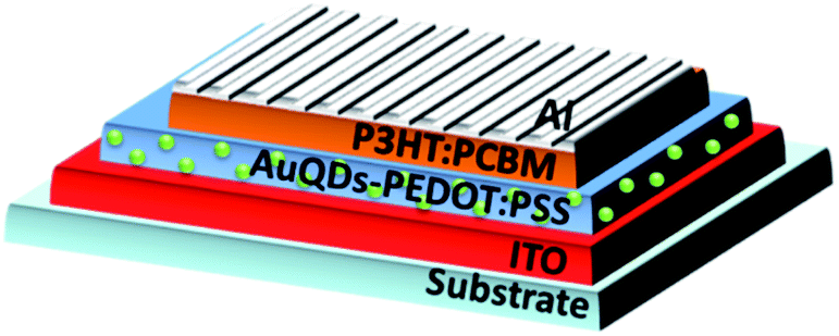 | ||
| Fig. 1 Schematic diagram of the fabricated green-AuQD/grating structured OSC device. | ||
Characterization
The surface morphology and thickness of the fabricated film were measured using atomic force microscopy (AFM, SPM-9600 Shimadzu). The electrical properties of the fabricated OSCs were characterized using a precision source/measure unit (B2901A, Agilent) and a potentiostat (PARSTAT 4000, Princeton Applied Research) under the irradiation of a solar simulator (75 mW cm−2, HAL-C100, Asahi Spectra, USA Inc.). The optical properties of fabricated OSCs measured in the reflection mode were recorded by using a homemade reflectometer that was made using a halogen light source (HL-2000, Ocean Optics, Inc.), a motorized rotating stage, and a UV-VIS spectrometer (USB200-TR, Ocean Optics, Inc.).Results and discussion
AuQDs absorb photons with a wavelength shorter than 400 nm and emit visible light. Depending on the number of gold atoms in the nanoclusters,44 green-AuQDs emit fluorescent light at a wavelength of 520 nm, which matches the strong absorption region of the photoactive layer of P3HT:PCBM (Fig. S4†).50,52 Of note, P3HT:PCBM has considerably weaker absorption and photoelectric conversion properties in the UV range than those in the visible range. Thus, green-AuQDs were employed as a photosensitizer to harvest the irradiated photons in the UV region and improve the OSC performance by the emission of visible light.In the fabricated OSCs, green-AuQDs were loaded into a liquid dispersion of PEDOT:PSS. The fluorescence emission of green-AuQDs in the mixture was easily monitored under UV light illumination (Fig. S5†). This implies that the fluorescence properties of AuQDs remain even after the AuQDs were loaded into the PEDOT:PSS medium. After the deposition of a HTL on the ITO electrode by spin coating, the surface morphology of the HTL with AuQDs was observed by AFM. Fig. 2(a) and (b) show that the HTL formed from PEDOT:PSS exhibits a flat surface, while the surfaces of the HTL films prepared from AuQD-loaded PEDOT:PSS contained small domains (∼0.25 nm in height) of aggregated AuQDs, as observed in the previous report.50 Using an appropriate loading amount, the AuQD particles can be homogenously blended into the HTL film. However, during the spin coating, the rapid evaporation of the solvent induced the agglomeration of dispersed particles, which left aggregated small domains of AuQDs on the surface of the HTL film.
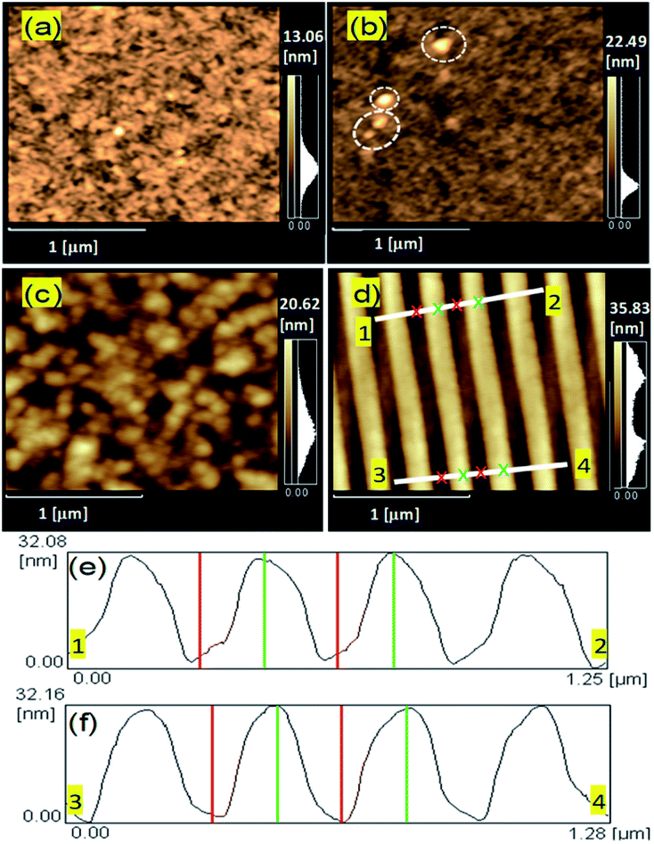 | ||
| Fig. 2 AFM images of the HTL films prepared from (a) PEDOT:PSS and (b) green-AuQD-loaded PEDOT:PSS. The white circles in (b) indicate the domains of aggregated green-AuQDs. AFM images of the (c) flat and (d) BD-R imprinted photoactive layers. (e) and (f) AFM line profiles that correspond to lines 1–2 and 3–4 in (f), respectively. | ||
In plasmonic OSCs, the introduction of nanostructures (e.g., nanopillars, honeycomb lattice, and periodic grating) on the surfaces of the active layer can increase the trapped light inside the OSC devices.5,9,16–18,53 We created the photoactive layer using the BD-R grating structures. After spin coating a polymer blend (P3HT:PCBM) on the surface of the HTL film, the BD-R grating pattern was created using capillary-assisted nanoimprinting. In this method, PDMS with a negative grating pattern was placed on the surface of the photoactive layer. The residual solvent, which is left in the film, and the thermal annealing at a temperature higher than Tg of the blend (100 °C) are the key parameters to promote the viscous state of the polymers, which facilitates the flow of viscous polymers into the grating grooves, which is driven by the capillary force.5,53Fig. 2(c) and (d) clearly show that the BD-R grating pattern was completely transferred onto the photoactive layer. The grating height and pitch on the imprinted surfaces were ∼32 and ∼320 nm (Fig. 2(e) and (f)), respectively. When the aluminum film was deposited on the photoactive layer, the corrugated nanopatterns were retained, which allowed to form a plasmonic grating located at the aluminum/photoactive layer interface of the OSC device, which consisted of an ITO/green-AuQD:PEDOT:PSS/P3HT:PCBM/Al grating structure. The grating structure of aluminum was confirmed by the AFM image of the aluminum surface (Fig. S6†).
The optical activities of fabricated OSCs were investigated. To confirm the excitation of GCSPR in OSCs, the reflection spectra of OSCs at various incident angles (20–60°) were recorded under the illumination of p-polarized (p-pol) white light, as shown in Fig. 3. Compared to the flat OSC, the improvement in the optical absorption due to light scattering was observed in the devices containing green-AuQDs and a BD-R grating. Furthermore, an additional optical absorption from GCSPR in the range of 650–800 nm was observed in the devices with BD-R. The results confirm that surface plasmons can be excited with a p-pol light irradiation in this configuration (i.e., the 1D grating direction is perpendicularly aligned).
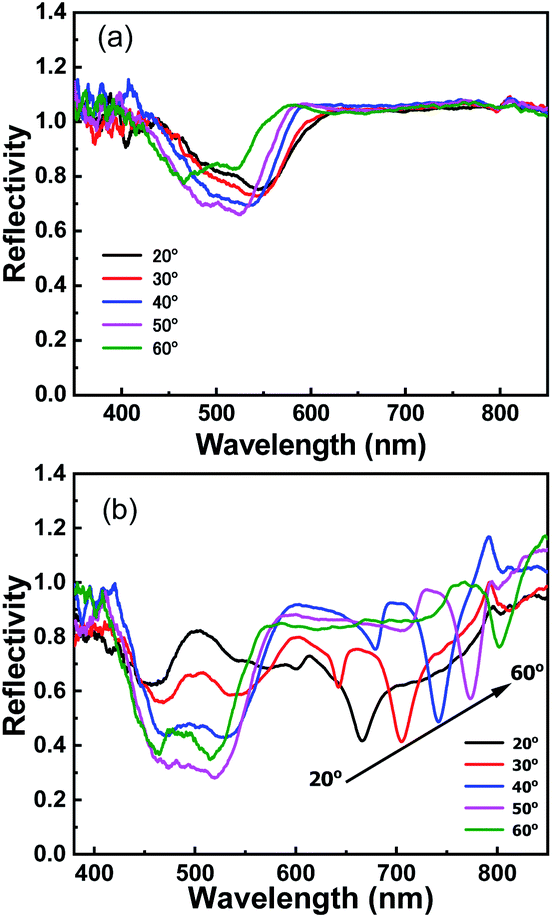 | ||
| Fig. 3 Reflectivity curves of (a) flat and (b) green-AuQD/BD-R OSCs. The reflectivity curves were recorded at various incident angles under p-pol light illumination. | ||
The OSC performance was investigated under the illumination of a non-polarized light with an intensity of 75 mW cm−2. The J–V properties and electrical parameters of the fabricated devices are shown in Fig. 4 and Table 1, respectively. The flat OSC (reference cell) exhibits the values of short circuit photocurrent (JSC), open circuit voltage (VOC), fill factor (FF), and efficiency (η) of 7.37 mA cm−2, 0.61 V, 0.54%, and 3.27%, respectively. Compared to the values of the reference cell, the OSC containing green-AuQDs in the HTL (green-AuQD OSC) exhibits better OSC performance. The presence of green-AuQDs provides a considerable improvement in JSC and η from 7.37 to 7.83 mA.cm−2 and 3.27 to 3.54%, respectively, which results in the efficiency enhancement of 8.26%. The value of VOC did not significantly change. These results correspond well with those in the previous report.50 In the case of green-AuQD OSC, the loaded green-AuQDs in the HTL absorb high energy photons in the UV region and emit visible light into the neighboring photoactive layer.49 In addition, by matching the fluorescence emission maximum of the loaded AuQDs to the absorption maximum wavelength of the photoactive layer, it is possible to achieve a considerable enhancement. As shown in Fig. S7 and Table S1,† when the AuQDs with blue (blue-AuQDs, Au5 and Au8; 5 and 8 Au atoms) and red fluorescence color (red-AuQDs, Au25; 25 Au atoms) were loaded into the HTL layer of the OSC, a lower performance enhancement was observed compared to that of green-AuQDs (Au13; 13 Au atoms). This observation is attributed to the fluorescence emission maximum of blue- and red-AuQDs matching the absorption maximum wavelength of P3HT:PCBM.51
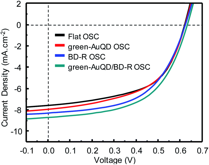 | ||
| Fig. 4 J–V characteristics of the fabricated OSCs under illumination with an intensity of 75 mW cm−2. The OSCs were illuminated at the normal incidence angle. | ||
| Devices | Electrical parameters | ||||
|---|---|---|---|---|---|
| J SC (mA cm−2) | V OC (V) | FF (%) | IPCE (%) | IPCE enhancement (%) | |
| Flat OSC | 7.37 ± 0.08 | 0.61 | 0.54 | 3.27 ± 0.03 | — |
| Green-AuQD OSC | 7.83 ± 0.07 | 0.62 | 0.54 | 3.54 ± 0.04 | 8.26 |
| BD-R OSC | 7.89 ± 0.05 | 0.63 | 0.54 | 3.61 ± 0.02 | 10.40 |
| Green-AuQD/BD-R OSC | 8.41 ± 0.11 | 0.62 | 0.55 | 3.91 ± 0.04 | 19.57 |
A further improvement in the OSC performance was observed in the grating structured OSCs. The integration of a plasmonic grating into the OSCs increased the values of JSC, FF, and IPCE to 7.89 mA.cm−2, 0.54%, and 3.61%, respectively, which resulted in the performance enhancement of 10.40%. Compared to that of AuQDs, a plasmonic BD-R grating provides a better enhancement in OSCs, Table 1. When a plasmonic grating is created on the surface of a photoactive layer, light scattering at the grating surface increases the effective light traveling path of incident photons in the photoactive layer. Meanwhile, GCSPR enhances the production of photo generated excitons.5,17,18 Thus, a 10.40% improvement in the OSC performance was achieved. We further investigated the use of green-AuQDs and a plasmonic BD-R grating to create a multiple enhancement effect in OSCs. As shown in Fig. 3 and Table 1, the green-AuQD/BD-R OSC provided a promising enhancement effect on OSCs. The green-AuQD/BD-R OSC produced JSC, FF, and IPCE values of 8.41 mA cm−2, 0.55%, and 3.91%, respectively. The utilization of green-AuQD and plasmonic BD-R produced an improvement of 19.57%.
To obtain better insight into how green-AuQDs and a plasmonic grating enhance JSC and the efficiency of fabricated devices, we evaluated the incident photon-to-current efficiency (IPCE) characterization (Fig. S8†). The incorporation of green-AuQD and plasmonic BD-R produce better IPCE enhancement than those of green-AuQD and BD-R OSCs. The IPCE enhancement factors were obtained by dividing the IPCE values of the green-AuQD-plasmonic grating OSC by the IPCE values of the reference solar cell, and were plotted against the incident light wavelength from 380 nm to 900 nm at various incident angles, as shown in Fig. 5. In this plot, the IPCE enhancement with a value greater than one indicates the improvement in IPCE compared to that of the reference OSC. For the green-AuQD OSC [Fig. 5(a)], the photovoltaic devices clearly exhibited an enhancement in IPCE over a wide wavelength range. The improvement in IPCE at 380–450 nm is attributed to the effect of green-AuQDs, which act as a photosensitizer harvesting photons in UV and near UV regions. Meanwhile, the green-AuQD particles can also scatter the incident light, which leads to the enhancement of IPCE over a wide wavelength range from 450 to 900 nm.
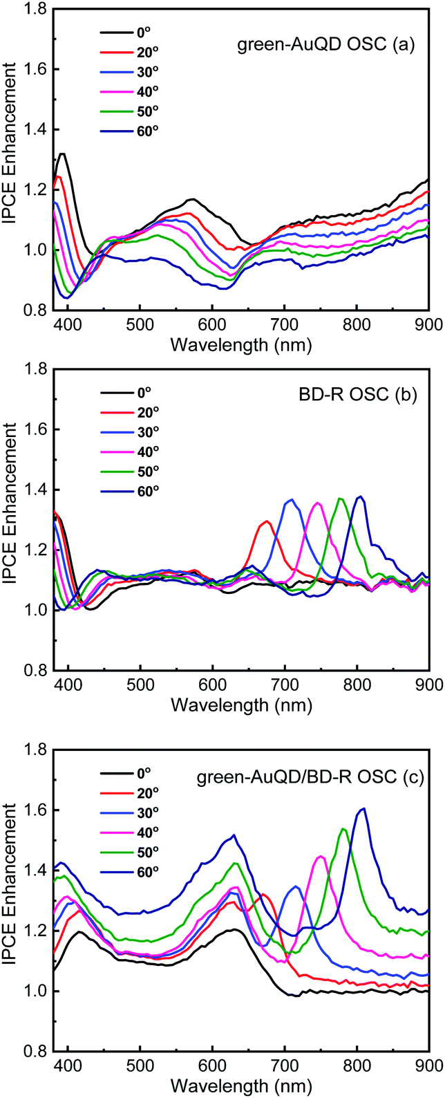 | ||
| Fig. 5 IPCE enhancement spectra of green-AuQD/BD-R OSCs under the irradiation of non-polarized light at various angles of incidence. (a) Green-AuQDs OSC, (b) BD-R OSC and (c) green-AuQD/BD-R OSC. | ||
Plasmonic grating enhances the performance by light scattering and GCSPR, as shown in Fig. 5(b).5 An IPCE improvement via light scattering was observed for the wavelength range of 380–650 nm, while the GCSPR provided an IPCE enhancement at a wavelength longer than 650 nm. By changing incident angles, the IPCE enhancement peak is tuned in the region of 650–800 nm. Because the enhancement peak wavelength corresponds to the GCSPR excitation peak wavelength, this result indicates that the GC-SPR indeed enhances the ICPE. In addition, thermal annealing and nanoimprinting with appropriate nanostructures can affect the P3HT chain alignment and the performance of photovoltaic devices.54–56 Fig. S9† shows that the as-cast P3HT:PCBM film exhibits a weak XRD peak at 5.35°, which is attributed to the (100) reflection of P3HT.57 After thermal annealing, the reflection peak at 5.35° increased, which indicates a well-organized polymer chain with an α-axis orientation. However, XRD characterization suggests that nanoimprinting did not provide a significant change in the P3HT chain alignment (Fig. S9 and S10†). Thus, the improvement in the OSC performance observed in the BD-R OSC is attributed to the optical effect of the plasmonic BD-R grating.
The incorporation of green-AuQD and a plasmonic BD-R provides the best IPCE enhancement compared to that using green-AuQD and BD-R OSCs. As shown in Fig. 5(c), green-AuQDs improve photon absorption at 380–450 nm.46,50 The enhancement effect owing to the strong light scattering by the BD-R grating and green-AuQD particles was observed for the wavelength range of 380–650 nm. The GCSPR effect from the BD-R grating produced an IPCE enhancement at the wavelengths longer than 650 nm.11 The IPCE enhancement peak is tuned by changing the angle of incidence, indicating that the IPCE enhancement wavelength depends on the GCSPR excitation wavelength.
The analysis of the charge transport resistance and the kinetics of the electron transfer of the fabricated devices were further investigated using electrochemical impedance spectroscopy. Fig. 6(a) shows the Nyquist plots of the fabricated OSCs, which exhibit the same semicircular characteristic for all devices. The series resistance (Rs) represents the resistive losses in ITO and PEDOT:PSS.4,36 The results show that the Rs values of the devices containing green-AuQDs and grating are not significantly different from those of the flat OSC. Interestingly, a lower charge transfer resistance (Rct) was observed in the OSCs with green-AuQDs and a plasmonic grating structure. While the flat OSC has the Rct value of 10.4 Ω, the green-AuQD, BD-R, and green-AuQD/BD-R OSC exhibit lower Rct values of 8.4, 8.4, and 6.6 Ω, respectively. The abovementioned results suggest that the use of green-AuQDs and a plasmonic grating can enhance the charge transfer in OSC. We further analyzed the characteristic frequency peaks and calculated an average electron lifetime (τavg). Fig. 6(b) and Table S2† show the characteristic frequency peaks of the Bode phase plots and calculated τavg, respectively. The results clearly demonstrate the insignificant difference in the τavg values in all devices. This implies that the use of green-AuQDs and a plasmonic BD-R grating does not affect the electron lifetime. An improvement in the OSC performance primarily originates from the enhancement in the photo-carrier generation rather than from the extension of the electron lifetime.
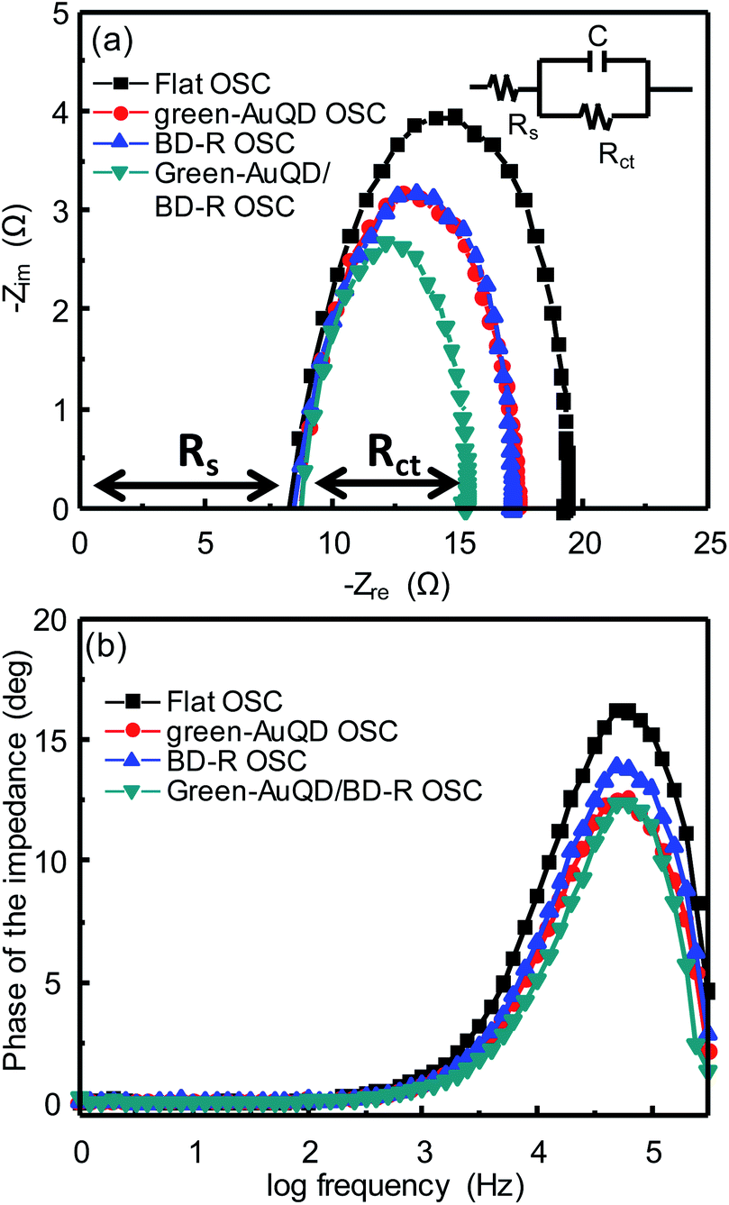 | ||
| Fig. 6 (a) Nyquist plots and (b) Bode phase plots of the fabricated OSCs. Electrochemical impedance spectroscopy (EIS) was performed under illumination with an intensity of 75 mW cm−2. The inset in (a) illustrates the equivalent circuit model of the fabricated OSC. | ||
As discussed above, the improvement in the OSC performance was achieved when green-AuQDs and a plasmonic BD-R grating were separately introduced into OSCs. Furthermore, the combination of green-AuQDs and a plasmonic BD-R grating results in an even greater enhancement in OSCs. When the GCSPR is excited, a strong enhanced electric field is generated near the surface. The enhanced electric field from the GCSPR enhances the fluorescence if the fluorophore material is located within the GCSPR evanescent field.58 We also observed the enhancement in the fluorescence emission of green-AuQDs by GCSPR of the plasmonic BD-R grating. As shown in Fig. 7(a), the improvement in the fluorescence emission of AuQDs was observed only for the Al-coated BD-R substrate. The maximum fluorescence enhancement was observed at an angle of incidence of 5° where the GCSPR excitation wavelength overlaps with the absorption wavelength of green-AuQDs and gradually disappears when the GCSPR excitation wavelength shifts from the absorption wavelength of green-AuQDs (Fig. 7(a), S4, and S11†). However, in the case of green-AuQDs on P3HT:PCBM on an Al grating [Fig. 7(b)], we did not observe the enhancement in the fluorescence emission originating from GCSPR. This result is obtained because the green-AuQDs on P3HT:PCBM are located far away from the surface of a plasmonic BD-R gating. Nevertheless, the GCSPR peaks, which were obtained from OSCs with a BD-R grating, did not overlap with the absorption of AuQDs. Thus, the enhancement effect observed for green-AuQD/BD-R OSCs originated separately from green-AuQDs and a plasmonic BD-R grating.
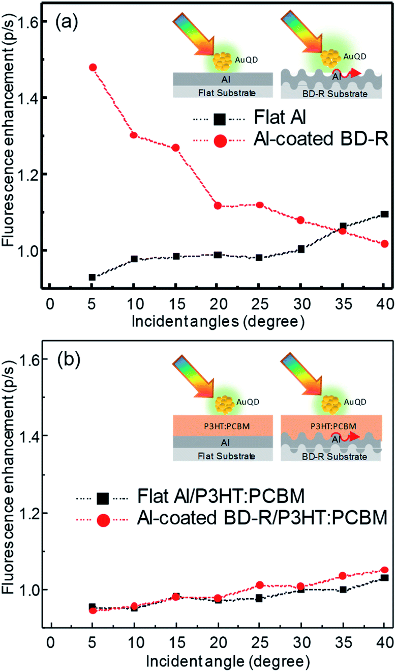 | ||
| Fig. 7 (a) Fluorescence enhancement (p/s) spectra of G-AuQDs deposited on a flat Al film and an Al-coated BD-R. (b) Fluorescence enhancement (p/s) spectra of G-AuQDs deposited on a flat Al/P3HT:PCBM film and an Al-coated BD-R/P3HT:PCBM film. The fluorescence of G-AuQDs at 530 nm was recorded under illumination with a wavelength of 350–500 nm. | ||
Conclusions
We used green-AuQDs and a plasmonic BD-R grating to successfully improve the performance of OSCs. The combination of green-AuQDs and a plasmonic BD-R grating was introduced for the first time and produced a superior enhancement. The insertion of green-AuQDs into the HTL resulted in an efficiency improvement of 8.26%, while the use of plasmonic BD-R resulted in a performance enhancement of up to 10.40%. Green-AuQDs can absorb light in the UV region and emit visible light into the neighboring active layer, which results in increased light harvesting by OSCs. In addition, green-AuQDs in the HTL can act as a scattering object trap for the incident light in the photoactive layer. A plasmonic BD-R grating enhances the optical absorption by light scattering and GCSPR. The combination of green-AuQDs and BD-R generate a considerable efficiency improvement of 19.57%. Our investigation provides the light manipulation strategy in OSCs using AuQDs and a plasmonic grating. This approach is promising and can be used for other related applications.Conflicts of interest
There are no conflicts to declare.Acknowledgements
This work was supported by the Japan Society for the Promotion of Science (JSPS) KAKENHI Grant Numbers JP16K13662 and JP17H03231. S. P. would like to thank the Science Achievement Scholarship of Thailand (SAST). S. N. gratefully thanks the JSPS for the Postdoctoral Fellowship and the Development and Promotion of Science and Technology Talents Project (DPST), Thailand. This research work was partially supported by Chiang Mai University (CMU). K. O. would like to thank the Research Center on Chemistry for Development of Health Promoting Products from Northern Resources, the Graduate School (CMU), the Center of Excellence for Innovation in Chemistry (PERCH-CIC) and the Department of Chemistry, Faculty of Science (CMU), and Center of Excellence in Materials Science and Technology (CMU).Notes and references
- C.-H. Chou and F.-C. Chen, Nanoscale, 2014, 6, 8444 RSC.
- X. Li, W. C. H. Choy, L. Huo, F. Xie, W. E. I. Sha, B. Ding, X. Guo, Y. Li, J. Hou, J. You and Y. Yang, Adv. Mater., 2012, 24, 3046 CrossRef CAS PubMed.
- W. C. H. Choy, Chem. Commun., 2014, 50, 11984 RSC.
- B. J. Leever, C. A. Bailey, T. J. Marks, M. C. Hersam and M. F. Durstock, Adv. Energy Mater., 2012, 2, 120 CrossRef CAS.
- S. Nootchanat, A. Pangdam, R. Ishikawa, K. Wongravee, K. Shinbo, K. Kato, F. Kaneko, S. Ekgasit and A. Baba, Nanoscale, 2017, 9, 4963 RSC.
- M. Notarianni, K. Vernon, A. Chou, M. Aljada, J. Liu and N. Motta, Sol. Energy, 2014, 106, 23 CrossRef CAS.
- C. J. Brabec, S. Gowrisanker, J. J. M. Halls, D. Laird, S. Jia and S. P. Williams, Adv. Mater., 2010, 22, 3839 CrossRef CAS PubMed.
- J. Yang, J. You, C.-C. Chen, W.-C. Hsu, H.-r. Tan, X. W. Zhang, Z. Hong and Y. Yang, ACS Nano, 2011, 5, 6210 CrossRef CAS PubMed.
- G. Luo, X. Ren, S. Zhang, H. Wu, W. C. H. Choy, Z. He and Y. Cao, Small, 2016, 12, 1547 CrossRef CAS PubMed.
- X. Li, W. C. H. Choy, H. Lu, W. E. I. Sha and A. H. P. Ho, Adv. Funct. Mater., 2013, 23, 2728 CrossRef CAS.
- X. Li, X. Ren, F. Xie, Y. Zhang, T. Xu, B. Wei and W. C. H. Choy, Adv. Opt. Mater., 2015, 3, 1220 CrossRef CAS.
- H. A. Atwater and A. Polman, Nat. Mater., 2010, 9, 205 CrossRef CAS PubMed.
- W. Wang, S. Wu, K. Reinhardt, Y. Lu and S. Chen, Nano Lett., 2010, 10, 2012 CrossRef CAS PubMed.
- M. Aryal, K. Trivedi and W. Hu, ACS Nano, 2009, 3, 3085 CrossRef CAS PubMed.
- J. Y. Park, N. R. Hendricks and K. R. Carter, Langmuir, 2011, 27, 11251 CrossRef CAS PubMed.
- J. You, X. Li, F.-x. Xie, W. E. I. Sha, J. H. W. Kwong, G. Li, W. C. H. Choy and Y. Yang, Adv. Energy Mater., 2012, 2, 1203 CrossRef CAS.
- A. Baba, N. Aoki, K. Shinbo, K. Kato and F. Kaneko, ACS Appl. Mater. Interfaces, 2011, 3, 2080 CrossRef CAS PubMed.
- K. Hara, C. Lertvachirapaiboon, R. Ishikawa, Y. Ohdaira, K. Shinbo, K. Kato, F. Kaneko and A. Baba, Phys. Chem. Chem. Phys., 2017, 19, 2791 RSC.
- A. Baba, K. Wakatsuki, K. Shinbo, K. Kato and F. Kaneko, J. Mater. Chem., 2011, 21, 16436 RSC.
- S. Nootchanat, H. Ninsonti, A. Baba, S. Ekgasit, C. Thammacharoen, K. Shinbo, K. Kato and F. Kaneko, Phys. Chem. Chem. Phys., 2014, 16, 24484 RSC.
- J. Zhu, M. Xue, R. Hoekstra, F. Xiu, B. Zeng and K. L. Wang, Nanoscale, 2012, 4, 1978 RSC.
- C. C. D. Wang, W. C. H. Choy, C. Duan, D. D. S. Fung, W. E. I. Sha, F.-X. Xie, F. Huang and Y. Cao, J. Mater. Chem., 2012, 22, 1206 RSC.
- Y.-S. Hsiao, S. Charan, F.-Y. Wu, F.-C. Chien, C.-W. Chu, P. Chen and F.-C. Chen, J. Phys. Chem. C, 2012, 116, 20731 CrossRef CAS.
- M. Sharma, P. R. Pudasaini, F. Ruiz-Zepeda, E. Vinogradova and A. A. Ayon, ACS Appl. Mater. Interfaces, 2014, 6, 15472 CrossRef CAS PubMed.
- A. Pangdam, S. Nootchanat, R. Ishikawa, K. Shinbo, K. Kato, F. Kaneko, C. Thammacharoen, S. Ekgasit and A. Baba, Phys. Chem. Chem. Phys., 2016, 18, 18500 RSC.
- E. Stratakis and E. Kymakis, Mater. Today, 2013, 16, 133 CrossRef CAS.
- P. Mandal and S. Sharma, Renewable Sustainable Energy Rev., 2016, 65, 537 CrossRef CAS.
- Y. H. Jang, Y. J. Jang, S. Kim, L. N. Quan, K. Chung and D. H. Kim, Chem. Rev., 2016, 116, 14982 CrossRef CAS PubMed.
- F. Enrichi, A. Quandt and G. C. Righini, Renewable Sustainable Energy Rev., 2018, 82, 2433 CrossRef CAS.
- K. Ueno, T. Oshikiri, Q. Sun, X. Shi and H. Misawa, Chem. Rev., 2018, 118, 2955 CrossRef CAS PubMed.
- M. A. Green, Y. Hishikawa, E. D. Dunlop, D. H. Levi, J. Hohl-Ebinger and A. W. Y. Ho-Baillie, Prog. Photovoltaics, 2018, 26, 3 Search PubMed.
- W. Na, M. Kang, D. Jang and S. Shin, Sens. Actuators, B, 2018, 254, 64 CrossRef CAS.
- J. Weickert, R. B. Dunbar, H. C. Hesse, W. Wiedemann and L. Schmidt-Mende, Adv. Mater., 2011, 23, 1810 CrossRef CAS PubMed.
- W.-H. Tseng, C.-Y. Chiu, S.-W. Chou, H.-C. Chen, M.-L. Tsai, Y.-C. Kuo, D.-H. Lien, Y.-C. Tsao, K.-Y. Huang, C.-T. Yeh, J.-H. He, C.-I. Wu, M. H. Huang and P.-T. Chou, J. Phys. Chem. C, 2015, 119, 7554 CrossRef CAS.
- C.-M. Liu, C.-M. Chen, Y.-W. Su, S.-M. Wang and K.-H. Wei, Org. Electron., 2013, 14, 2476 CrossRef CAS.
- A. Ng, W. K. Yiu, Y. Foo, Q. Shen, A. Bejaoui, Y. Zhao, H. C. Gokkaya, A. B. Djurišić, J. A. Zapien, W. K. Chan and C. Surya, ACS Appl. Mater. Interfaces, 2014, 6, 20676 CrossRef CAS PubMed.
- L. Lu, Z. Luo, T. Xu and L. Yu, Nano Lett., 2013, 13, 59 CrossRef CAS PubMed.
- M.-K. Chuang and F.-C. Chen, ACS Appl. Mater. Interfaces, 2015, 7, 7397 CrossRef CAS PubMed.
- T. Putnin, C. Lertvachirapaiboon, R. Ishikawa, K. Shinbo, K. Kato, S. Ekgasit, K. Ounnunkad and A. Baba, Opto-Electron. Adv., 2019, 2, 190010 Search PubMed.
- A. Kogo, Y. Takahashi, N. Sakai and T. Tatsuma, Nanoscale, 2013, 5, 7855 RSC.
- K. G. Stamplecoskie and P. V. Kamat, J. Phys. Chem. Lett., 2015, 6, 1870 CrossRef CAS PubMed.
- K. G. Stamplecoskie, Y.-S. Chen and P. V. Kamat, J. Phys. Chem. C, 2014, 118, 1370 CrossRef CAS.
- U. Uddayasankar and U. J. Krull, Langmuir, 2015, 31, 8194 CrossRef CAS PubMed.
- S. Eustis and M. A. El-Sayed, Chem. Soc. Rev., 2006, 35, 209 RSC.
- L.-Y. Chen, C.-W. Wang, Z. Yuan and H.-T. Chang, Anal. Chem., 2015, 87, 216 CrossRef CAS PubMed.
- J. Zheng, C. Zhang and R. M. Dickson, Phys. Rev. Lett., 2004, 93, 077402 CrossRef PubMed.
- N. Sakai and T. Tatsuma, Adv. Mater., 2010, 22, 3185 CrossRef CAS PubMed.
- H. Choi, Y.-S. Chen, K. G. Stamplecoskie and P. V. Kamat, J. Phys. Chem. Lett., 2015, 6, 217 CrossRef CAS PubMed.
- M. A. Abbas, T.-Y. Kim, S. U. Lee, Y. S. Kang and J. H. Bang, J. Am. Chem. Soc., 2016, 138, 390 CrossRef CAS PubMed.
- A. Pangdam, S. Nootchanat, C. Lertvachirapaiboon, R. Ishikawa, K. Shinbo, K. Kato, F. Kaneko, S. Ekgasit and A. Baba, Part. Part. Syst. Charact., 2017, 34, 1700133 CrossRef.
- S. Phetsang, A. Phengdaam, C. Lertvachirapaiboon, R. Ishikawa, K. Shinbo, K. Kato, P. Mungkornasawakul, K. Ounnunkad and A. Baba, Nanoscale Adv., 2019, 1, 792 RSC.
- P. Vanlaeke, A. Swinnen, I. Haeldermans, G. Vanhoyland, T. Aernouts, D. Cheyns, C. Deibel, J. D'Haen, P. Heremans, J. Poortmans and J. V. Manca, Sol. Energy Mater. Sol. Cells, 2006, 90, 2150 CrossRef CAS.
- Y. Yang, K. Mielczarek, M. Aryal, A. Zakhidov and W. Hu, ACS Nano, 2012, 6, 2877 CrossRef CAS PubMed.
- Y. Yang, K. Mielczarek, M. Aryal, A. Zakhidov and W. Hu, Nanoscale, 2014, 6, 7576 RSC.
- E. Verploegen, C. E. Miller, K. Schmidt, Z. Bao and M. F. Toney, Chem. Mater., 2012, 24, 3923 CrossRef CAS.
- E. Verploegen, R. Mondal, C. J. Bettinger, S. Sok, M. F. Toney and Z. Bao, Adv. Funct. Mater., 2010, 20, 3519 CrossRef CAS.
- D. E. Motaung, G. F. Malgas, S. S. Nkosi, G. H. Mhlongo, B. W. Mwakikunga, T. Malwela, C. J. Arendse, T. F. G. Muller and F. R. Cummings, J. Mater. Sci., 2013, 48, 1763 CrossRef CAS.
- A. Baba, K. Kanda, T. Ohno, Y. Ohdaira, K. Shinbo, K. Kato and F. Kaneko, Jpn. J. Appl. Phys., 2010, 49, 01AE02 CrossRef.
Footnotes |
| † Electronic supplementary information (ESI) available: AFM images of devices. Schematic diagram of the OSC fabrication process. UV-Vis absorption and a fluorescence spectrum of a green-AuQD solution. J–V characteristics of the AuQD-loaded OSCs under illumination with an intensity of 75 mW cm−2. The OSCs were illuminated at the normal incidence angle. Incident photon-to-current efficiency (IPCE) spectra of fabricated OSCs measured at 30° under the irradiation of a non-polarized light. X-ray diffraction (XRD) patterns of the P3HT:PCBM film cast on glass substrates. XRD patterns of the BD-R imprinted P3HT:PCBM film recorded with a different orientation toward the XRD scanning plane. Reflectivity curves (p/s) of a green-AuQD thin film. See DOI: 10.1039/d0na00169d |
| ‡ Present Addresses: Advanced Research Laboratories, Tokyo City University, 8-15-1 Todoroki, Setagaya-ku, Tokyo 158-0082, Japan. |
| This journal is © The Royal Society of Chemistry 2020 |