
 Open Access Article
 This Open Access Article is licensed under a Creative Commons Attribution-Non Commercial 3.0 Unported Licence
Comparative study of femtosecond laser-induced structural colorization in water and air
Erik M.
Garcell
a,
Subhash C.
Singh
 ab,
Huiyan
Li
a,
Bin
Wang
b,
Sohail A.
Jalil
ab and
Chunlei
Guo
*ab
ab,
Huiyan
Li
a,
Bin
Wang
b,
Sohail A.
Jalil
ab and
Chunlei
Guo
*ab
aThe Institute of Optics, University of Rochester, Rochester, NY 14627, USA. E-mail: guo@optics.rochester.edu
bChangchun Institute of Optics, Fine Mechanics and Physics, Chinese Academy of Science, Changchun 130033, China
First published on 1st June 2020
Abstract
The study of femtosecond laser structural coloring has recently attracted a great amount of research interest. These studies, however, have only been carried out in air. At the same time, laser ablation has also been actively studied in liquids as they provide a unique environment for material processing. However, surprisingly, structural coloring has never been performed in liquids. In this work, we perform the first study of metal structural coloring in liquid and compare the results to metal structural coloring in air. Colors created in liquid are formed by nanoparticle-induced plasmonic absorption and result in a range of colors transitioning from purple to orange. Surface structures formed in liquid are less hierarchical and more uniform than those formed in air, producing a surface with a much higher reflectance due to reduced light trapping, resulting in a more vibrant color. However, colorization formed in water suffers from less uniform colorization due to turbulence at the air–water and water-target interfaces, resulting in slight changes to the laser beam's focus during processing. Finally, finite-difference-time-domain simulation based on the measured surface structures is used to understand the role of plasmonic resonance in colorization.
1. Introduction
Colorization of solid surfaces using plasmonic effects of nanostructures, known as structural coloring, has attracted great interest because of their applications in non-additive coloring or decorating surfaces with high values where conventional pigment or paint should be avoided for several reasons such as counterfeiting, environmental hazard, additional mass, and short lifetime of these coatings.1–4 Several fabrication methods such as electron beam lithography, interference lithography, ion beam lithography, and milling and nanoimprint lithography are used to realize structural colors.5–9 However, these methods exhibit a slow fabrication process, need highly precise and costly equipment, and are limited to flat working surfaces, therefore are not suitable for the large-scale production of cost-effective colored surfaces. Moreover, the colors produced from the periodic nanopatterns fabricated by these techniques are generally iridescent i.e. angle-dependent.10Laser-induced metal colorization is a form of material functionalization. By ablating the surface of a metal, a series of micro and nanostructures can be formed, that through direct light absorption, multiple reflections, and plasmonic resonance, can tune the reflection profile of metals making them appear a different color.11–14 Femtosecond pulsed lasers are particularly useful in this task due to their small heat-affected zones, and high peak intensities, allowing for the formation of dense and high aspect ratio micro and nanostructured surfaces.15,16 We and other groups widely used femtosecond laser surface processing in the air to produce highly absorptive, so-called “black metals”,13,17 and surfaces that reflect specific color i.e. “colored metals”.11,18–20 Pulsed laser ablation in liquid (PLAL), where laser beam irradiates target surface at solid–liquid interface through a transparent liquid has a number of advantages over ablation in air/vacuum including smoother surfaces and edges in laser cutting and drilling,21,22 higher rate of material removal, plasma-induced etching of material surface, formation of colloidal solution of nanoparticles (NPs), and surface functionalization.21–27 However, mostly PLAL research is focused on the formation of colloidal solution of NPs either using laser ablation of bulk metal target and solid–liquid interface21–26 or laser-induced melting/fragmentation of suspended nanoparticles for their resizing and reshaping,27 and surprisingly has been never used for the structural coloring of surfaces. To the best of our knowledge, this is the first report on the liquid-phase laser-induced structural coloring of the surface of any material.
Here, we demonstrate femtosecond laser-induced structural colorization of copper surface in water and air and explain the plasmonic colorization mechanism through the combination of experimental hemispherical optical reflectance and numerical simulation. By varying the average incident pulse number per unit area on the Cu surface, we produced a range of colors from purple to orange. Through optical reflectance and nanoparticle analyses, we study these structures and directly compare them to similarly femtosecond laser colorized Cu in air. Finally, finite-difference-time-domain (FDTD) simulation is used to understand the role of plasmonic resonance in copper colorization.
2. Experimental and optical simulation
All samples in this study were irradiated using a pulsed Ti:sapphire laser system operating at 800 nm central wavelength with linear polarization, 53 fs pulse width, and 1 kHz repetition rate. For liquid ablation experiment: the sample was mounted on a platform at the center of an acrylic cubical box filled with double distilled water. The water reservoir with the sample was translated in the x–y plane using a computer-controlled dual-axis translation stage (Fig. 1(a)). The laser beam (fluence = 5.4 J cm−2) was focused on the sample surface through a 5 mm thick water layer using a 100 mm focal length plano-convex lens. For ablation in air, the sample was mounted on a vertical x–y translational stage and irradiated with a laser fluence of 5.6 J cm−2. In both cases, 1 mm thick polished Cu foils were used as starting surface. The laser beam was unidirectional raster scanned on the sample surface with 100 μm interline spacing and 100 μm spot size. The average laser energy delivered at a given spot and hence the size and morphology of structures produced at that spot is controlled by scanning speed of the laser beam. The surface morphology of the irradiated samples was studied using a scanning electron microscope (SEM). PerkinElmer Lambda 365 double beam spectrophotometer equipped with a 50 mm integrating sphere was used for hemispherical reflectance measurements of the laser processed colored copper samples.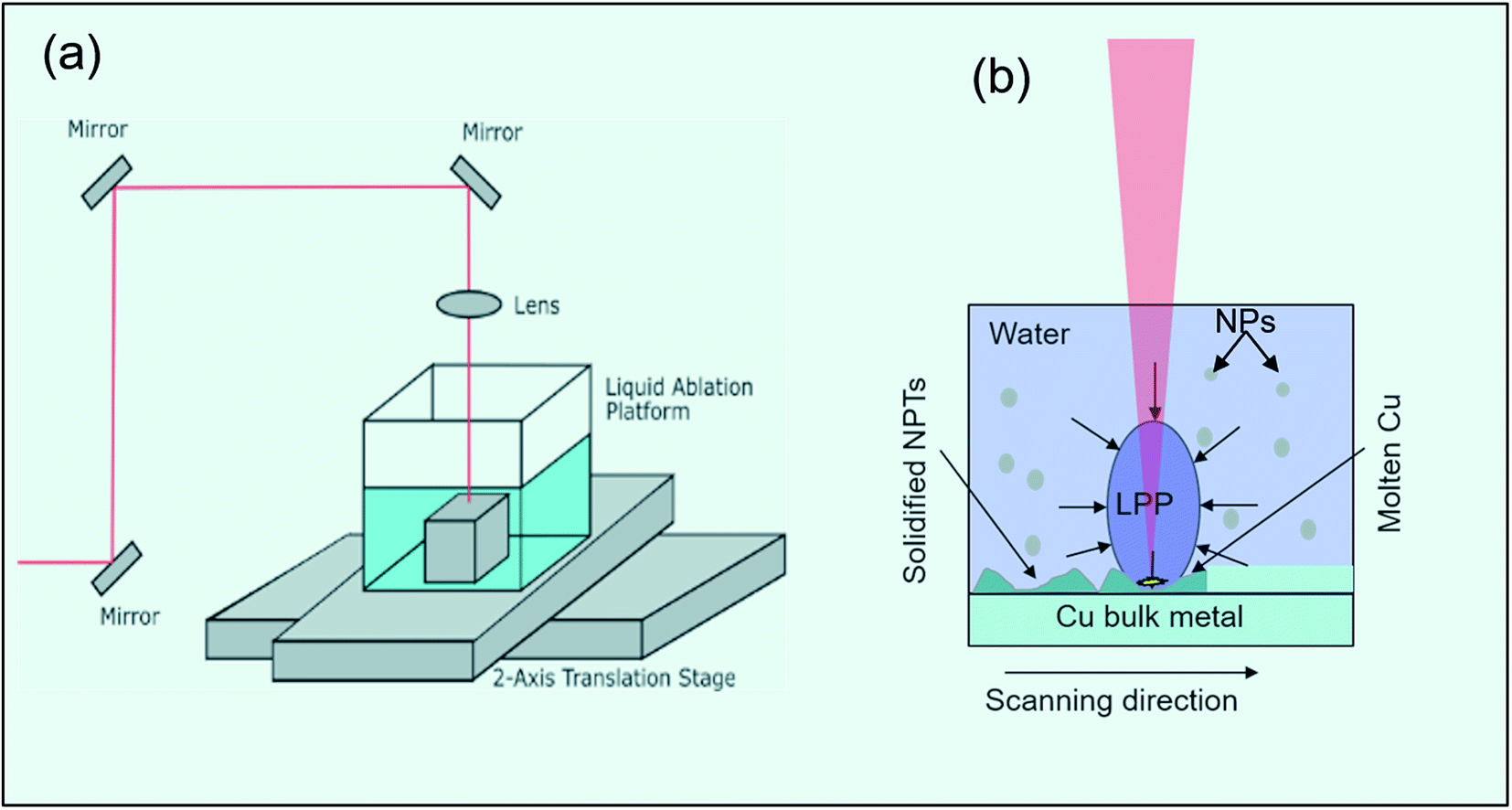 | ||
| Fig. 1 (a) Experimental setup of liquid-phase femtosecond laser induced structural colorization, (b) schematic for laser produced plasma (LPP) induced pressure that pushes molten material to produced hemispherical NPTs on copper surface. | ||
For FDTD simulation, a commercial FDTD package known as Lumerical solutions (Lumerical Inc.) was used to calculate the spectral response of E-field distribution on reflection monitor. An array of copper nano-protrusions (NPTs) with average size and separation extracted from SEM images was designed on the copper substrate. A normally incident broadband unpolarized light in the spectral range of 400–800 nm was considered as a light source, and periodic boundary conditions were used in the x and y directions, while the phase-matched layer (PML) was used in the z-direction.
3. Results and discussion
By increasing the laser scanning speed from 0.5 to 2 mm s−1, a range of colors can be formed on Cu following femtosecond laser ablation in water (Fig. 2(a–d)). Raster scanning faster or slower than this range yielded ablated samples with either no visible ablation or a dulled grey colorization, respectively. Colors formed shows transition from a deep purple at 0.5 mm s−1 to a light orange at 2 mm s−1 scanning speed. These colors are similar to those formed after laser surface processing of copper in the air (top of Fig. 3). Colors formed in the air are produced using a comparable laser fluence to that used for liquid ablation but require faster scanning speeds to produce similar colorization, 3 mm s−1 to 4 mm s−1. The wave-like patterns observed on the surface of the Cu samples ablated in water are variations in the apparent color. These are neither due to variations in ablation depth nor as a result of material transport. This change in color on the Cu surface is most likely a consequence of the translation stage's movement, as observed before,28 perturbing the water–air and water-target interfaces that probably altered the laser beam's effective focus position and produced areas of local color difference on the Cu surface. The appearance of the wavelike pattern is more intense at higher scanning speed that supports our speculation. The wavelike pattern can be avoided to produce a more uniform color by scanning the laser beam at a fixed water-target interface instead of scanning of the target at a fixed laser beam position, as shown in ref. 29 in the formation of LIPSS through fs laser ablation in water. Another possibility of the non-uniform appearance in the color may be due to the scattering and refraction of the laser beam from persistent bubbles, nucleate and grow due to the laser-heating of the target surface and incubation effect, that reduces the overall laser power reaching at the target surface.30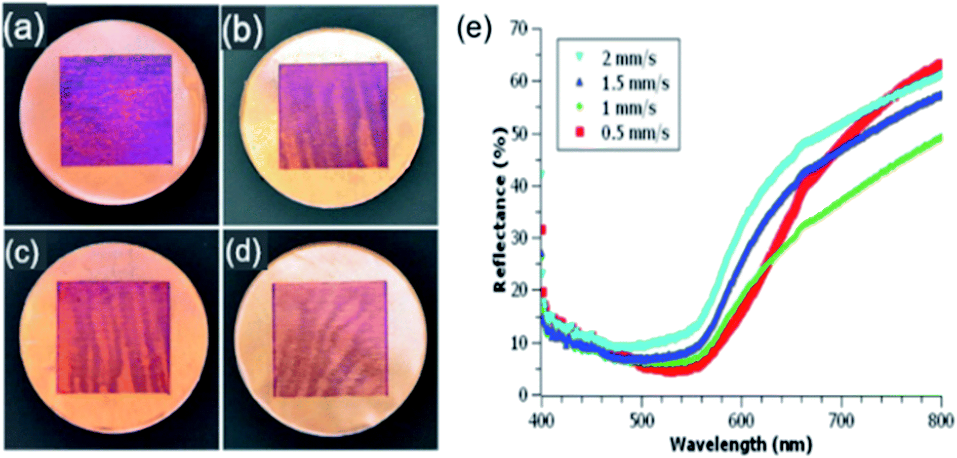 | ||
| Fig. 2 Photographs of colored copper samples irradiated in double distilled water with laser scanning speeds (a) 0.5 (b) 1.0 (c) 1.5 and (d) 2.0 mm s−1. (e) Reflectance spectra of colored copper samples produced at different scan speeds. | ||
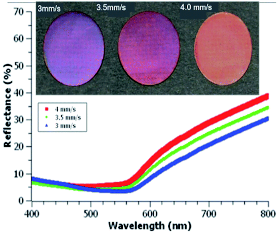 | ||
| Fig. 3 Colored copper samples irradiated in air at scanning speeds (left to right) 3 mm s−1, 3.5 mm s−1, 4 mm s−1, and corresponding reflectance spectra (bottom). | ||
The hemispherical spectral reflectance of the colored copper samples produced by pulsed laser ablation (PLA) in double distilled water is shown in Fig. 2(e). Compared to one another, samples irradiated with scanning speeds between 1 to 2 mm s−1 exhibit the same overall spectral shape but tends towards decreased reflectance for slower scanning speeds. Instead of following this same trend, samples irradiated with 0.5 mm s−1 scanning speed (red curve) exhibit comparatively higher absorption in the spectral range of 480 nm–640 nm along with a larger reflection at a longer wavelength that explains its deep purple appearance. As compared to the sample produced at 0.5 mm s−1 scanning speed, copper surface processed with 1 mm s−1 scan speed has slightly higher reflectance in the visible (480–640 nm), but much lower reflectance at longer wavelengths (green curve) that gives it an orange color. Comparing reflectance spectra of liquid-phase laser ablated samples to that of the similarly colored air ablated samples (see the top of Fig. 3), liquid ablated samples have much higher reflectance. Previous works also show similarly low reflectance spectra for colorized air ablated Cu17,18 and other metals.31 Faster scanning speeds are required for air ablated Cu to form colors similar to those formed in water. Having used comparable initial fluences, this difference in required scanning speeds is likely due to water having a greater absorption than air at 800 nm wavelength. Due to this increased absorption, a larger number of pulses hence a slower scanning speed is required to achieve similar colorization results.
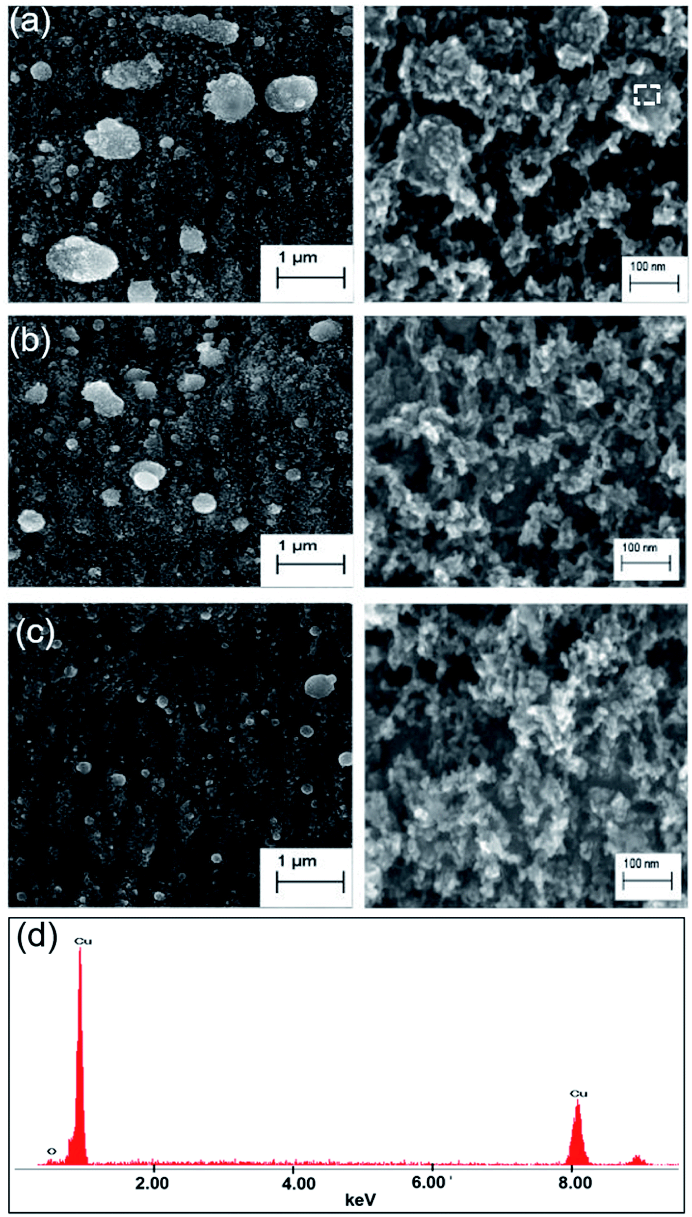
Surface morphological investigation of the liquid ablated samples under SEM shows the growth of an array of hemispherical nano-protrusions (NPTs) on the copper surface, where the size of these nano-protrusions decreases and wall-to-wall separation between them increases with increase in the scanning speed (Fig. 4(a–d)). These NPTs are possibly formed through high pressure exerted by liquid-confined-copper-plasma at the molten-copper beneath it followed by ultrafast cooling and re-solidification (Fig. 1(b)). Spatial confinement of laser-produced plasmas (LPPs) generally increase temperature, pressure and kinetic energy of the plasma species.32 The LPPs, spatially confined by transparent water overlayer, interact and push its surrounding interfaces and the molten metal layer beneath it. The size of NPTs produced on the target surface depends on the amount of molten metal beneath the LPP that itself depends on the amount of deposited laser energy per unit area at the solid–liquid interface. A higher scan speed of 2.0 mm s−1 corresponds to an average of 50 laser pulses at the focus spot area of 100 μm, while a slower scan speed of 0.5 mm s−1 results in an average of 200 laser pulses in the same area. The smaller amount of deposited laser pulse energy on the target surface for higher scan speed (2.0 mm s−1) results in the formation of smaller size NPTs (Fig. 4(d)). Dotted encircled regions in Fig. 4 show either deposition of copper oxide NPs on the surface or in the gap regions of NPTs (right panels of Fig. 4(a–c)) or formation of small size of copper oxide NPTs (right panel of Fig. 4(d)). It is interesting to note that several smaller sized copper oxide NPTs are formed on the copper surface with higher scan speed (right panel of Fig. 4(d)), while several smaller sized (5–20 nm) copper oxide NPs are deposited on the surface of Cu NPTs structured at lower scan speed (right panel of Fig. 4(a)). The density of deposited copper oxide NPs increases with a decrease in the scan speed. Generally, metal oxide nanoparticles (NPs) forms at the plasma–water interface are dispersed into liquid and have a lesser probability to get redeposit at the target surface. Therefore, structures formed at the copper surface by laser ablation in water has a much smoother surface with lower oxide content as compared to those produced in the air (see EDAX images Fig. 4(e) and 5(d)). Fast Fourier Transform (FFT) analysis of these surfaces shows the spatial period (av. dia. of NPT + wall-to-wall separation) of NPTs from ∼140 to ∼170 nm (inset Fig. 4(b) and (c)). These quasi-periodic arrays of NPTs induce an anti-reflective effect at wavelengths close to four-times of their period (Fig. 2(e)). An increase in the scanning speed slightly decreases the period of NPTs array resulting in shorter wavelength shifts in the resonance absorption and appearance of a reddish color. EDAX image of the sample prepared at 0.5 mm s−1 scanning speed, shown in Fig. 4(e), shows <2% of the oxygen content.
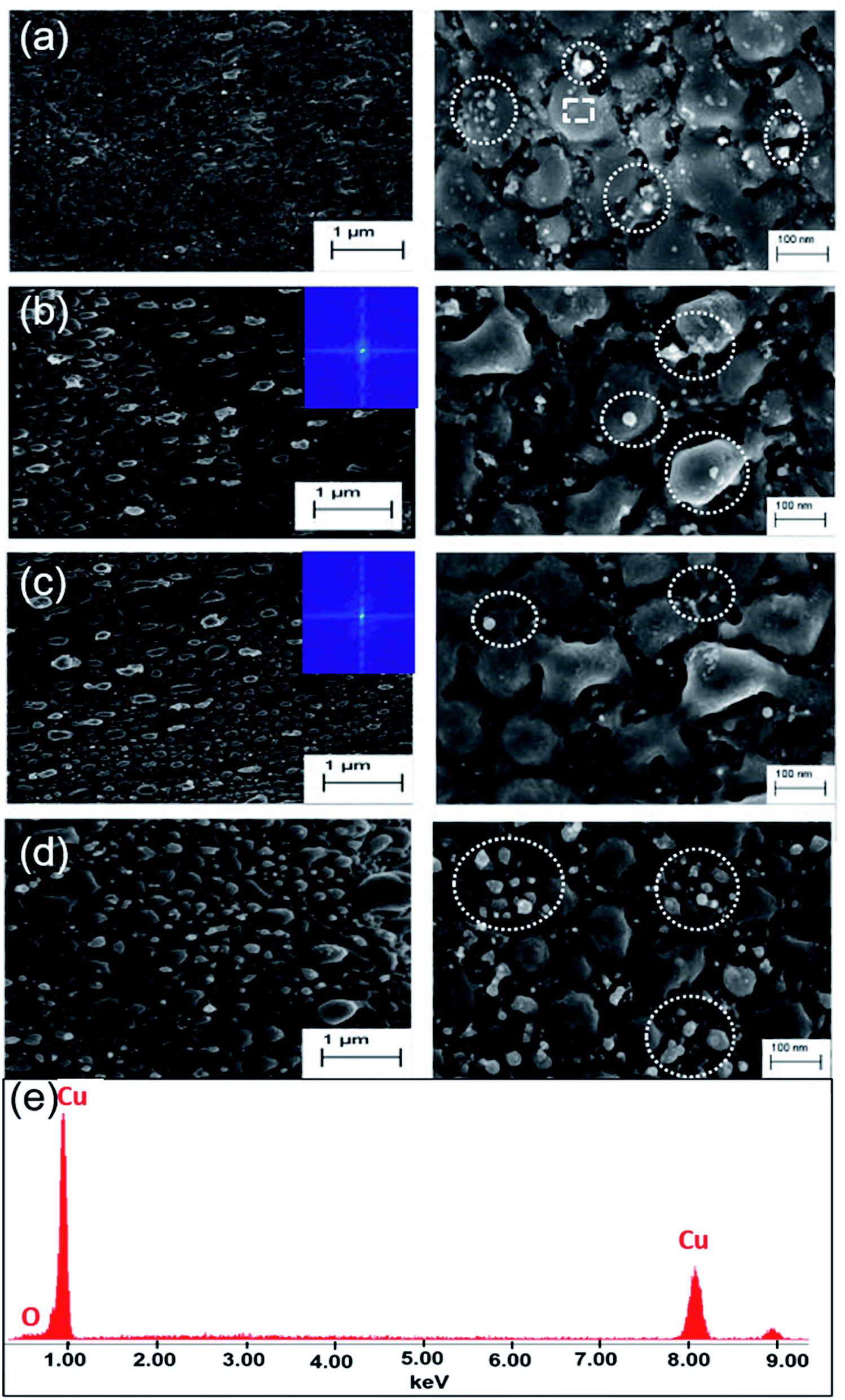 | ||
| Fig. 4 SEM images of copper samples, ablated in double distilled water with laser scanning speeds of (a) 0.5, (b) 1.0, (c) 1.5, and (d) 2.0 mm s−1 at scale bars of 1 μm (left) and 100 nm (right). Encircled regions in the right show deposition of small copper oxide NPs (5–20 nm) on the surface of NPTs. Insets (b) and (c) show corresponding fast-Fourier-transform images. (e) EDAX image of the square region in the SEM image of the surface processed with 0.5 mm s−1 scan speed. | ||
 | ||
| Fig. 5 SEM images of the colored copper samples laser processed in air with the scanning speeds of (a) 3.0, (b) 3.5, and (c) 4.0 mm s−1. Scale bars 1 μm (left) and 100 nm (right). (d) EDAX image of the colored copper sample produced at 3.0 mm s−1 scan speed. | ||
In contrast to liquid-phase ablation, Cu surfaces laser processed in the air are covered with dense layers of redeposited NPs and their self-assembled hierarchical nanostructures (Fig. 5(a–c)). The left panels of these images show zoomed out views of the irradiated samples, better illustrating the uniformity (liquid ablation), or lack thereof (air ablation), of NPs on the ablated Cu surface. The redeposition of ablated material causes the surface of air-ablated samples to exhibit a wider distribution in NPs sizes. The wider NP size distribution, along with the formation of hierarchical structures is likely the cause of the decreased reflectance of air-ablated Cu as compared to one ablated in liquid, for similar colors. The larger nanoparticle distribution excites a more broadband plasmonic absorption, while the hierarchical nanostructures trap light in cavities and absorb light by means of angular dependent Fresnel absorption.13,33 Laser-induced periodic surface structures (LIPSS) (left panels Fig. 5(a–c)), observed only in the case of air ablated samples, can scatter light to contribute towards the overall reduced reflectance over the water ablated samples.17 The EDAX image of the sample prepared at 3 mm s−1 scanning speed, shown in Fig. 5(d), demonstrate <5% oxygen content in the sample. For both air and liquid ablation, overall reflectance is further reduced by antireflection effects caused by the graded effective refractive index at the air–metal interface due to the random subwavelength structures formed on the Cu surface following ablation.34
Size of periodic nanostructures and their period determine position and intensity of surface plasmon resonance modes35 and hence structural colorization. To understand this, we carefully analyze and extract the mean radius and interparticle separation of NPTs from SEM images of colored samples produced by PLA in double-distilled water. Analysis of the water ablation Cu samples reveals that, for increasing laser beam scanning speeds, the average size of NPTs decreases, but a larger number of NPTs are formed (Fig. 6(a)). At slower scanning speeds, the irradiated sample is receiving a larger number of average pulses per unit area, which has been shown to increase the size of NPTs and decrease in the number of NPTs formed.17,36 With an increase in the number of pulses at a given spot, the smaller size of NPTs formed from previous pulses melted, got coalescence and formed the larger size of NPTs. Although an increased number of NPTs are formed at larger scanning speeds, due to a decrease in the average NPTs size the average interparticle spacing increases (Fig. 6(a and b)). Due to an extremely hierarchical nature and high density of NPs in the air ablated Cu, the statistical analysis of nanoparticles formed on the surface of the air processed colored copper sample is not possible. However, from SEM images shown in Fig. 5, one can see a similar trend of smaller NPs formation with higher scanning speed. The study of NPs for Cu ablated in the air has been extensively studied and shows similar results to those of liquid ablated Cu where faster scanning speeds resulting in a smaller average NPs size and a larger interparticle separation.18,37,38
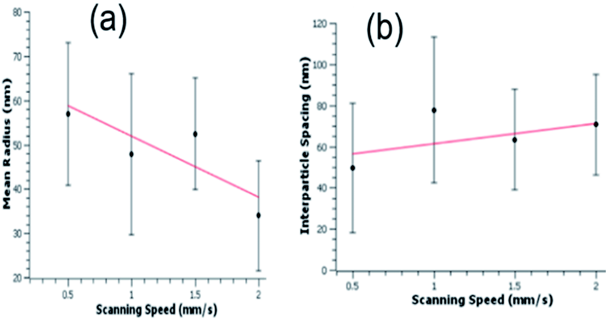 | ||
| Fig. 6 (a) Average particle size, and (b) average interparticle distance on the surface of copper after fs laser processing in double water with different scanning speeds. Error bars show range of smallest and largest size of NPTs on the colored copper surface processes at corresponding scan speed. | ||
To further understand and support our claim for the mechanism of structural coloring in the present case, we numerically simulated optical reflectance from an array of hemispherical Cu NPTs on perfectly flat Cu substrate illuminated with a normal incident broadband unpolarized light source. Three sets of nanostructured surfaces with arrays of Cu NPTs of (i) diameter (D) = 60 nm and wall-to-wall spacing (d) = 70 nm (corresponding to SEM image Fig. 4(d)), (ii) D = 120 nm, d = 50 nm (corresponding to SEM image Fig. 4(a)) without redeposited NPs, and (iii) D = 120 nm, d = 50 nm with smaller sized copper NPs (D = 20 nm, d = 10 nm) are designed. Here, first, we ignored the oxidation of copper NPTs and considered the deposition of copper NPs on the surface. Simulated reflectance spectra for all the three cases show resonance absorption at 550 nm with an overall spectral shape very similar to our experimental reflectance shown in Fig. 2(e). Similar to experimental results, the simulated reflectance peak close to 550 nm shows higher absorption and a longer wavelength shift with an increase in the size of NPTs and a decrease in the interparticle spacing (slower scanning case). From Fig. 7(a), we can see that an increase in the particle size from D = 60 nm to D = 120 nm causes decrease in the reflectance from ∼58% to ∼33% at 550 nm wavelength resulting ∼43% sensitivity ( where R0 and D0 are initial reflectance from the structure and diameter of the NPT). The presence of smaller sized NPs on the surface and in the interparticle gap in the SEM image of Fig. 4(a) encouraged us to study effects of these NPs (D = 20 nm, d = 10 nm) on the spectral reflectance. The addition of copper NPs further decreases absorption near 550 nm and slightly shifts resonance absorption towards longer wavelengths. However, the change in the absorption due to the addition of smaller sized NPs is much smaller as compared to the change in the size of NPTs. Surface processed with slower scanning speeds results in a larger density of smaller sized NPs (Fig. 4(a)) that slightly increases total absorbance around 550 nm (Fig. 2(e); red curve) for slower processed sample. Electric-field distribution (Fig. 7(b–d)) also shows higher absorption at 550 nm wavelength for larger sized NPTs with smaller interparticle spacing (Fig. 7(c)). The addition of smaller sized NPs further increases near-field interaction and hence absorption at 550 nm (Fig. 7(d)). Near-field coupling between NPs hybridizes the plasmonic modes and generate electromagnetic resonances at longer wavelengths that broadens the spectral absorption profile.39
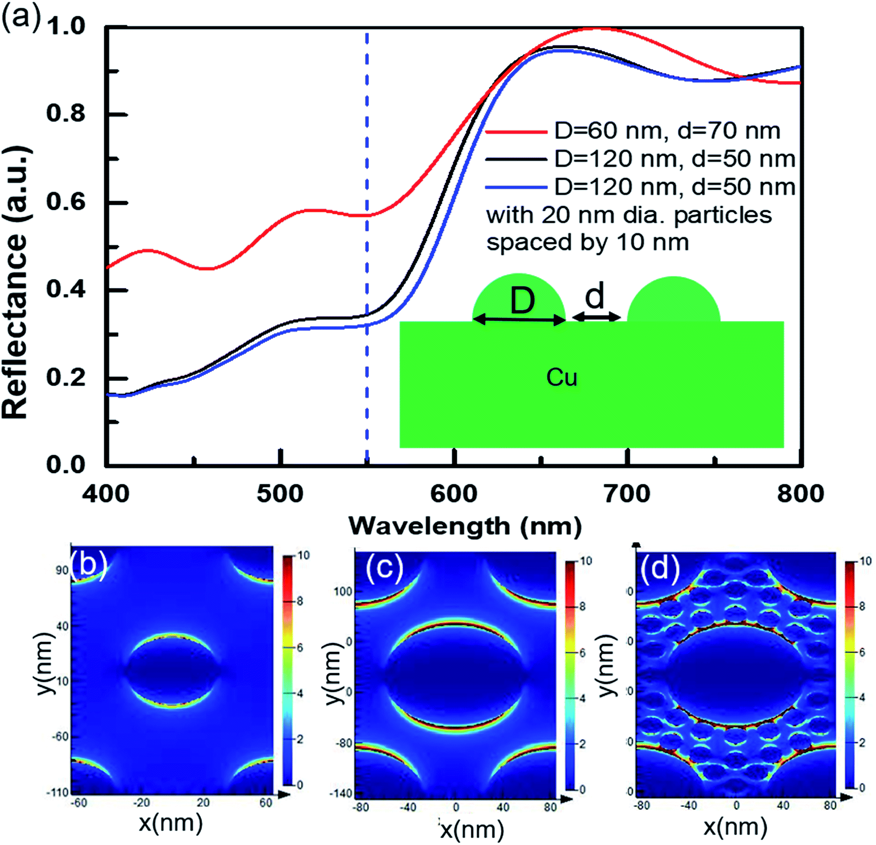 | ||
| Fig. 7 (a) FDTD simulation for spectral reflectance from an array of Cu corresponding to surfaces produced with 0.5 and 2.0 mm scan speeds. Electric field distribution for λ = 550 nm light at 2 nm above the copper substrate around NPTs of (b) D = 60 nm, d = 70 nm, (c) D = 120 nm, d = 50 nm, and (d) smaller sized NPs around D = 120 nm, d = 50 nm NPTs. | ||
It is well known that laser ablation of active metals, such as zinc and copper, in water generates their oxide NPs and makes a thin layer of oxide on the target surface.22,23 It is also verified from the appearance of lighter NPTs (encircled region Fig. 4(d)) and lighter NPs (encircled regions Fig. 4(a–c) in the SEM images. Since electron density in metal oxides is much lower as compared to corresponding metals, therefore in SEM imaging, a region with higher oxide content shows whitish appearance. We further studied the influences of the thin oxide shell layer on the surface of Cu NPTs and deposition of smaller sized spherical CuO NPs (SEM image Fig. 4(a) and EDAX image Fig. 4(e)) on the spectral absorption and hence plasmonic colorization. Arrays of hemispherical Cu core@CuO shell NPTs (inset Fig. 8(a) with fixed dimensions of (i) D = 60 nm and d = 70 nm (Fig. 8(a), and (ii) D = 120 nm, d = 50 nm (Fig. 8(b)) are designed and CuO shell layer thickness is varied in the range of 2 to 10 nm. It is interesting to note that for smaller as well as larger sized NPTs, absorbance at 550 nm slightly increased (i.e. 5% decrease in the reflectance; ∼55 to ∼50% for smaller size, and ∼10% from ∼35 to ∼25% for larger size NPTs) with (2 to 10 nm) increase in the CuO shell layer thickness. The results shows a maximum of 10% change in the absorbance for 400% change in the CuO shell layer thickness resulting ∼7% sensitivity (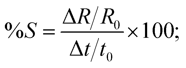 where Δt, and t0 are change in the shell layer thickness and initial shell thickness respectively). To further study the influence of CuO NPs in the gap region of Cu core@CuO shell NPTs on spectral absorbance, we considered 10 nm thick CuO shell layer and added CuO NPs of 5 to 20 nm in diameter in the gap region (Fig. 8(c) and (d)). For both cases, spectral absorbance at 550 nm slightly increased with an increase in the size of NPs (∼50 to ∼40% change in the reflectance for smaller, and ∼25 to ∼21% change in reflectance for larger size NPTs). A maximum of 10% change in the absorbance for 300% change in the particle size resulting 6.6% sensitivity. With the careful analysis of these simulation results, it seems that the size of CuO NPs has more influence on the array of smaller sized NPTs (Fig. 8(c)) over the larger one (Fig. 8(d), while the effect of shell layer thickness is more pronounced in the optical reflectance for larger sized NPTs (Fig. 8(b)) as compared to smaller ones (Fig. 8(a)). The FDTD simulation shows that the size of the NPTs and their separation, structural, has the highest contribution (S = 43%) in the colorization, while thickness of CuO shell layer and size of redeposited CuO NPs have much weaker dependence i.e. ∼7% and ∼6.6% sensitivities. The close resemblance of simulated reflectance from an array of Cu NPTs on the copper substrate with experimental results supports our claim of plasmonic colorization. From these simulations, we can say that the colorization largely depends on the size of NPTs (structural effect) rather than the oxidation (chemical effect) of the surfaces.
 | ||
| Fig. 8 FDTD simulation to investigate the influence of shell layer thickness in Cu core@CuO shell NPTs on optical reflectance for (a) D = 60 nm, d = 70 nm, and (b) D = 120 nm, d = 50 nm NPTs. FDTD simulation to investigate the influence of CuO spherical NPs around Cu core@CuO shell NPTs for (c) D = 60 nm, d = 70 nm, and (d) D = 120 nm, d = 50 nm NPTs. Arrangements of NPTs of 120 nm diameter and 50 nm interspacing with 20 nm diameter CuO NPs in the gap region, and corresponding spatial distribution of E-filed in the x–y plane are shown in the inset of (d). | ||
4. Conclusions and prospects
By varying the laser's scan speed, we successfully created four non-iridescent colors ranging from purple to orange on the surface of copper using femtosecond laser ablation in water. Compared to laser ablation in air, the reflection profiles for samples formed in water are on average twice as reflective, resulting in a much brighter apparent colorization. This can be attributed to both smaller nanoparticle sizes, and a lack of hierarchical structures, forming in water that would otherwise trap light. The different scanning speeds resulted in different colors on the material's surface which relate to the average diameter and spacing of Cu NPTs formed on the Cu surface. Higher scanning speed results in the formation of smaller size NPTs with larger spacing causing higher overall reflectance with an orange appearance. However, larger sized and closely spaced NPTs formed with slower scanning speed result in higher absorption with a purple appearance. The surface structure is modeled using average size and spacing obtained by SEM images to numerically simulate optical reflectance and understand the mechanism of colorization. At last, the colorization has much higher dependence on the size of NPTs (structural effect) as compared to the surface oxidation (i.e. compositional or chemical effect).Conflicts of interest
There are no conflicts to declare.Acknowledgements
We acknowledge financial supports from Bill & Melinda Gates Foundation (OPP1157723).References
- A. Kristensen, J. K. W. Yang, S. I. Bozhevolnyi, S. Link, P. Nordlander, N. J. Halas and N. A. Mortensen, Plasmonic colour generation, Nat. Rev. Mater., 2016, 2, 1–14 Search PubMed.
- T. Ellenbogen, K. Seo and K. B. Crozier, Chromatic, plasmonic polarizers for active visible color filtering and polarimetry, Nano Lett., 2012, 12, 1026–1031 CrossRef CAS.
- J. Olson, A. Manjavacas, L. Liu, W.-S. Chang, B. Foerster, N. S. King, M. W. Knight, P. Nordlander, N. J. Halas and S. Link, Vivid, full-color aluminum plasmonic pixels, Proc. Natl. Acad. Sci. U.S.A., 2014, 111, 14348–14353 CrossRef CAS PubMed.
- X. Chen, Y. Chen, J. Dai, M. Yan, D. Zhao, Q. Li and M. Qiu, Ordered Au nanocrystals on a substrate formed by light-induced rapid annealing, Nanoscale, 2014, 6, 1756–1762 RSC.
- K. Kumar, H. Duan, R. S. Hegde, S. C. W. Koh, J. N. Wei and J. K. W. Yang, Printing colour at the optical diffraction limit, Nat. Nanotechnol., 2012, 7, 557–561 CrossRef CAS PubMed.
- L. Duempelmann, D. Casari, A. Luu-Dinh, B. Gallinet and L. Novotny, Color rendering plasmonic aluminum substrates with angular symmetry, ACS Nano, 2015, 9, 12383–12391 CrossRef CAS PubMed.
- A. S. Roberts, A. Pors, O. Albrektsen and S. I. Bozhevolnyi, Subwavelength plasmonic color printing protected for ambient use, Nano Lett., 2014, 14, 783–787 CrossRef CAS PubMed.
- S. J. Tan, L. Zhang, D. Zhu, M. G. Xiao, Y. M. Wang, K. Kumar, C.-W. Qiu and J. K. W. Yang, Plasmonic color palettes for photorealistic printing with aluminum nanostructures, Nano Lett., 2014, 14, 4023–4029 CrossRef CAS PubMed.
- F. Cheng, J. Gao, L. Stan, D. Rosenmann, D. Czaplewski and X. Yang, Aluminum plasmonic metamaterials for structural color printing, Opt. Express, 2015, 23, 23279–23285 Search PubMed.
- J. S. Clausen, E. Højlund-Nielsen, A. B. Christiansen, S. Yazdi, M. Grajower, H. Taha, U. Levy, A. Kristensen and N. A. Mortensen, Plasmonic Metasurfaces for Coloration of Plastic Consumer Products, Nano Lett., 2014, 14, 4499–4504 CrossRef CAS PubMed.
- A. Y. Vorobyev and C. Guo, Colorizing metals with femtosecond laser pulses, Appl. Phys. Lett., 2008, 92, 041914 CrossRef.
- J.-M. Guay, A. C. Lesina, G. Côté, M. Charron, D. Poitras, L. Ramunno, P. Berini and A. Weck, Laser-induced plasmonic colours on metals, Nat. Commun., 2017, 8, 16095 CrossRef CAS PubMed.
- A. Y. Vorobyev and C. Guo, “Femtosecond laser blackening of metals,” in 2009 52nd IEEE International Midwest Symposium on Circuits and Systems, 2009, pp. 905–908 Search PubMed.
- A. Y. Vorobyev and C. Guo, Metallic light absorbers produced by femtosecond laser pulses, Adv. Mech. Eng., 2010, 2, 452749 CrossRef.
- S. A. Jalil, J. Yang, M. ElKabbash, C. Cong and C. Guo, Formation of controllable 1D and 2D periodic surface structures on cobalt by femtosecond double pulse laser irradiation, Appl. Phys. Lett., 2019, 115, 031601 CrossRef.
- S. A. Jalil, J. Yang, M. El-Kabbash, S. C. Singh and C. Guo, Maskless formation of uniform subwavelength periodic surface structures by double temporally-delayed femtosecond laser beams, Appl. Surf. Sci., 2019, 471, 516–520 CrossRef CAS; S. A. Jalil, M. Akram, J. A. Bhat, J. J. Hayes, S. C. Singh, M. ElKabbash and C. Guo, Creating superhydrophobic and antibacterial surfaces on gold by femtosecond laser pulses, Appl. Surf. Sci., 2020, 506, 144952–144958 CrossRef PubMed.
- A. Y. Vorobyev and C. Guo, Direct femtosecond laser surface nano/microstructuring and its applications, Laser Photon. Rev., 2013, 7, 385–407 CrossRef CAS.
- E. M. Garcell and C. Guo, Colorful multifunctional surfaces produced by femtosecond laser pulses, Opt. Mater. Express, 2019, 9, 1033–1040 CrossRef CAS.
- G. Li, J. Li, Y. Hu, C. Zhang, X. Li, J. Chu and W. Huang, Femtosecond laser color marking stainless steel surface with different wavelengths, Appl. Phys. A, 2015, 118, 1189 CrossRef CAS.
- Y. M. Andreeva, V. C. Luong, D. S. Lutoshina, O. S. Medvedev, Y. Yu. Mikhailovskii, M. K. Moskvin, G. V. Odintsova, V. V. Romanov, N. N. Shchedrina and V. P. Veiko, Laser coloration of metals in visual art and design, Opt. Mater. Express, 2018, 9, 1310 CrossRef.
- A. Kruusing, Handbook of liquids-assisted laser processing, Elsevier Science, 2007, ISBN: 9780080444987 Search PubMed.
- Nanomaterials: Processing and Characterization with Lasers, ed. S. C. Singh, H. Zeng, C. Guo and W. Cai, Wiley-VCH, 2012, ISBN: 978-3-527-32715-7 Search PubMed.
- H. Zeng, X. W. Du, S. C. Singh, S. A. Kulinich, J. He and W. Cai, Nanomaterials via laser ablation/irradiation in liquid: a review, Adv. Funct. Mater., 2012, 22, 1333 CrossRef CAS.
- D. Zhang, B. Gökce and S. Barcikowski, Laser Synthesis and Processing of Colloids: Fundamentals and Applications, Chem. Rev., 2017, 117, 3990 CrossRef CAS PubMed.
- R. K. Swarnkar, S. C. Singh and R. Gopal, Synthesis of Copper/Copper-Oxide Nanoparticles: Optical and Structural Characterizations, AIP Conf. Proc., 2009, 1147, 205 CrossRef CAS; S. C. Singh, Effect of oxygen injection on the size and compositional evolution of ZnO/Zn (OH)2 nanocomposite synthesized by pulsed laser ablation in distilled water, J. Nanopart. Res., 2011, 13, 4143 CrossRef.
- R. K. Swarnkar, S. C. Singh and R. Gopal, Optical characterizations of copper oxide nanomaterial, in Proceedings of the ICOP International Conference on Optics and photonics, CSIO, Chandigarh, 2009 Search PubMed.
- S. C. Singh, S. K. Mishra, R. K. Srivastava and R. Gopal, Optical properties of selenium quantum dots produced with laser irradiation of water suspended Se nanoparticles, J. Phys. Chem. C, 2010, 114, 17374–17384 CrossRef CAS.
- D. Zhang and K. Sugioka, Hierarchical microstructures with high spatial frequency laser induced periodic surface structures possessing different orientations created by femtosecond laser ablation of silicon in liquids, Opto Elec, Adv, 2019, 2, 900021–9000218 Search PubMed.
- R. Nadarajah, S. Barcikowaski and B. Gokce, Picosecond laser-induced surface structures on alloys in liquids and their influence on nanoparticle productivity during laser ablation, Opt. Express, 2020, 28, 2909 CrossRef PubMed.
- D. Zhang, B. Ranjan, T. Tanaka and K. Sugioka, Underwater persistent bubble-assisted femtosecond laser ablation for hierarchical micro/nanostructuring, Int. J. Extreme Manuf., 2020, 2, 015001 CrossRef.
- A. Y. Vorobyev and C. Guo, Reflection of femtosecond laser light in multipulse ablation of metals, J. Appl. Phys., 2011, 110, 043102 CrossRef.
- S. C. Singh, C. Fallon, P. Hayden, M. Mujawar, P. Yeates and J. T. Costello, Ion flux enhancements and oscillations in spatially confined laser produced aluminum plasmas, Phys. Plasmas, 2014, 21, 093113 CrossRef.
- A. Y. Vorobyev and C. Guo, Water sprints uphill on glass, J. Appl. Phys., 2010, 108, 123512 CrossRef.
- F. Ghmari, T. Ghbara, M. Laroche, R. Carminati and J.-J. Greffet, Influence of microroughness on emissivity, J. Appl. Phys., 2004, 96, 2656–2664 CrossRef CAS.
- B. Wang, S. C. Singh, H. Lu and C. Guo, Design of Aluminum Bow-tie Nanoantenna Array with Geometrical Control to Tune LSPR from UV to near-IR for Optical Sensing, Plasmonics, 2020, 15, 609–621 CrossRef CAS.
- A. Vorobyev and C. Guo, Femtosecond laser nanostructuring of metals, Opt. Express, 2006, 14, 2164–2169 CrossRef CAS.
- P. Fan, M. Zhong, L. Li, P. Schmitz, C. Lin, J. Long and H. Zhang, Angle-independent colorization of copper surfaces by simultaneous generation of picosecond-laser-induced nanostructures and redeposited nanoparticles, J. Appl. Phys., 2014, 115, 124302 CrossRef.
- P. Fan, M. Zhong, L. Li, P. Schmitz, C. Lin, J. Long and H. Zhang, Sequential color change on copper surfaces via micro/nano structure modification induced by a picosecond laser, J. Appl. Phys., 2013, 114, 083518 CrossRef.
- M. ElKabbash, A. Sousa-Castillo, Q. Nguyen, R. Mariño-Fernández, N. Hoffman, M. A. Correa-Duarte and G. Strangi, Tunable black gold: controlling the near-field coupling of immobilized Au nanoparticles embedded in mesoporous silica capsules, Adv. Opt. Mater., 2017, 5, 1700617 CrossRef.
| This journal is © The Royal Society of Chemistry 2020 |