
Scalable fabrication of a complementary logic inverter based on MoS2 fin-shaped field effect transistors†
Yann-Wen
Lan
 *a,
Po-Chun
Chen
a,
Yun-Yan
Lin
a,
Ming-Yang
Li
b,
Lain-Jong
Li
c,
Yu-Ling
Tu
b,
Fu-Liang
Yang
b,
Min-Cheng
Chen
d and
Kai-Shin
Li
*d
*a,
Po-Chun
Chen
a,
Yun-Yan
Lin
a,
Ming-Yang
Li
b,
Lain-Jong
Li
c,
Yu-Ling
Tu
b,
Fu-Liang
Yang
b,
Min-Cheng
Chen
d and
Kai-Shin
Li
*d
aDepartment of Physics, National Taiwan Normal University, Taipei 11677, Taiwan. E-mail: ywlanblue@gmail.com
bResearch Center for Applied Sciences, Academia Sinica, Taipei, Taiwan
cPhysical Sciences and Engineering Division, King Abdullah University of Science and Technology (KAUST), Thuwal, Kingdom of Saudi Arabia
dNational Nano Device Laboratories, National Applied Research Laboratories, Hsinchu 30078, Taiwan. E-mail: ksli@narlabs.org.tw
First published on 7th January 2019
Abstract
Integration of high performance n-type and p-type field-effect transistors with complementary device operation in the same kind of layered materials is highly desirable for pursuing low power and flexible next-generation electronics. In this work, we have shown a well-mannered growth of MoS2 on a fin-shaped oxide structure and integration of both n-type and p-type MoS2 by using a traditional implantation technique. With the advance of the fin-shaped structure, the maxima and the effective ON current density for the MoS2 fin-shaped field-effect transistors are respectively obtained to be about 50 μA μm−1 (normalized by the circumference of the fin) and around 500 μA μm−1 (only normalized by the fin size), while its ON/OFF ratio is more than 106 with low OFF current of a few pA. Based on our n-type and p-type MoS2 fin-shaped field-effect transistors, the complementary MoS2 inverter with a high DC voltage gain of more than 20 is acquired. Our results provide evidence for complementary 2D material operation in the same materials, a promising avenue for the development of high performance and high-density complementary 2D electronic devices.
Conceptual insightsIn this study, a new concept has been demonstrated, which is the integration of both fin-shaped n-type and p-type MoS2 field effect transistors by using a traditional implantation technique to show high performance two-dimensional material electronics. Compared to the existing research, this concept is compatible with the Si-based fabrication process and is industrially feasible for the future fabrication of advanced devices. The additional insight to the nanoscience field in this work is to provide a good idea (fin-shaped MoS2 FETs) for enhancing the effective current density to act as a promising protocol of new future CMOS applications. |
Moore's law states that the number of transistors in the same chip area doubles approximately every two years.1 This long-persisting law, however, is challenged by the existence of leakage current due to the short channel effect. In order to eliminate the short channel effect, scientists have executed several device constructions.2–4 A fin-shaped field effect transistor (fin-FET), one of the most popular designs, conducts fin-like channels forming a wrap-around gate structure and provides superior electrical control compared to planar structures.5 As a consequence, the leakage current can then be suppressed while the device performance is still augmented. Other methods such as applying new materials instead of silicon while scaling down the channel length of FETs are worthy of consideration. Two-dimensional (2D) layered materials such as transition metal dichalcogenides (TMDs) have received huge attention soon after the discovery of graphene.6 Physical properties such as electrical transport properties and flexibility endow TMDs with potential applications in electronic, spintronic and optical devices.7–12 TMDs as channel materials in future FET applications are one promising choice; among these materials, MoS2 is regarded as one of the candidates due to its atomically thin and flat nature as well as high mobility and large band gap.13–17 MoS2 itself, however, seems not suitable for acting as a complementary metal-oxide semiconductor (CMOS) since it generally shows only n-type behavior. Most reported CMOS configuration-based 2D layered materials use both MoS2 and WSe2 as n-type and p-type semiconductors, respectively.18,19 However, growing two materials in the same chip/wafer is too complicated for mass production, since it is hard to combine it with the current semiconductor fabrication process. The ideal case is similar to silicon and germanium, fabricating n-type and p-type channels on the same semiconductor material. Some people have reported that the change from n-type to p-type channel can be induced by ion implantation.20 Another way is to utilize a high work function material as a buffer layer contacting with the MoS2 film, leading to hole carriers dominating the MoS2 transport behavior. For example, Ali's group has succeeded in demonstrating a p-type MoS2 transistor with a MoOx/MoS2 contact.21
Since buffer layering is not a standard process and it may degrade the performance of devices during procedures, it is highly desirable to figure out the whole silicon compatibility in the fabrication process. There is a previous simulation study showing that MoS2 contacting with high work function silicon may bring about hole-dominated carrier injection in MoS2 FETs.22 Based on the implication of this study, we have meticulously fabricated devices and successfully demonstrated both n-type and p-type FETs made of MoS2 film in an identical chip by directly growing MoS2 on different types of source/drain silicon electrodes. Furthermore, in order to take advantage of its high current density, the MoS2 film is intentionally grown on the fin oxide structure. The chemical vapor deposition (CVD) of MoS2 can fully cover the fin oxide structure which is compatible with the Si-based fabrication process and is industrially feasible for the future fabrication of advanced devices. We have also shown that the complementary MoS2 (CMOS2) inverter has a dc voltage gain of more than 20. This CMOS2 is based on n-type and p-type MoS2 and is promising for acting as the protocol of new future CMOS applications.
The device fabrication in this work is extended from our previously reported study on the advanced 10 nm channel-length MoS2 devices.23 The main difference from our previous study, in terms of device geometry, is the fin-shaped structure for the channel. The whole process flow is completely described in Fig. S1 (ESI†). The typical MoS2 thin film islands and their Raman spectrum (A1g − E2g = 19 cm−1) are shown in Fig. S2 (ESI†), which indicates the presence of the crystal MoS2 film near the S/D electrodes. A schematic plot of the CVD system and the thermal cycle used for layered MoS2 deposition are shown in Fig. S3 (ESI†).24
Fig. 1(a) shows a schematic plot of a MoS2 fin-shaped field effect transistor (a MoS2 fin-FET), which displays an original idea that the SiO2 fin structure is fully covered with a continuous layered MoS2 film as a fin-shaped conduction channel. The top-view SEM image of one of the MoS2 fin-FETs is shown in Fig. 1(b), where the gate electrode crosses over between the source (S) and drain (D) with the surface contact area of about 300 nm2 and the distance between S and D is 100 nm. The cross-section TEM image shown in Fig. 1(c) clearly displays the fully oxidized SiO2 fin structure with layered MoS2 coverage with a high-k metal gate stack. Note that there is a thin SiO2 layer (∼3 nm) that we intentionally grow on top of the continuous 3 nm (5 layers) MoS2 film as the buffer layer for high quality HfO2 deposition, as shown in Fig. 1(d). Without this buffer layer, it is easy to damage the MoS2 film when an ALD process is conducted. In addition, the uniformity of the film still needs to be improved for future applications, so we suggest that the CVD setup with a vertical vapor flow could potentially be used for the synthesis of highly uniform MoS2 instead of the horizontal vapor flow we use now.
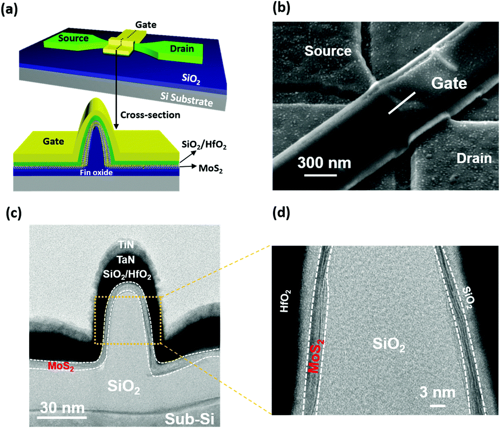 | ||
| Fig. 1 MoS2 fin-shaped field effect transistors. (a) Schematic plot of a MoS2 fin-shaped field effect transistor. (b) A top-view SEM image of a MoS2 fin-shaped field effect transistor. White lines in the center indicate the cutting position for a cross-section TEM inspection. (c) A cross-section TEM image of a MoS2 fin-shaped field effect transistor. (d) A high resolution TEM image of a MoS2 fin structure, showing the MoS2 thickness of about 3 nm (∼5 layers) in the MoS2 fin-shaped field effect transistors. | ||
During the fabrication process of the MoS2 fin-FET, we purposefully combine a traditional implantation technique into our process to make both n-type and p-type MoS2 conduction channels possible in the same 2D layered material. The mechanism enabling the acquisition of both the n- and p-type MoS2 conduction channel is proposed below. According to our previous experience of the Si-TMD contact, highly doped Si directly contacting with TMD materials is possible to adjust the channel chemical potential with respect to the original level. Owing to the dramatic formation of band bending in MoS2, the MoS2 Fermi level is effectively close to the conduction band by the n+ Si contact or the valence band by the p+ Si contact. The band diagrams for n-type and p-type contacts on the OFF state are separately shown in Fig. 2(a) and (c), which indicate that the electron and hole in two cases are blocked due to the energy barrier ϕn and ϕp respectively. On the contrary, the electron and the hole in both cases can transport as conducting carriers in the ON state while gate voltages are applied in the positive direction for the n-type contact and in the negative direction for the p-type contact as shown in Fig. 2(b) and (d), in which the gate voltage must at least overcome the energy barrier (i.e. Vth). In our experiments, since we selectively implant Si contacts as n+ Si and p+ Si for the seed to grow the MoS2 film on a wafer/chip, both n-type and p-type MoS2 conducting channels are expected to be simultaneously obtained in a run of the fabrication process.
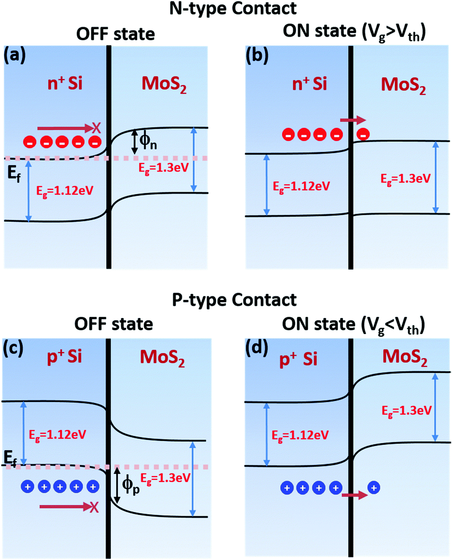 | ||
| Fig. 2 Band diagrams of highly doped Si contacts with MoS2 for p-type and n-type channel conduction. (a and b) MoS2 contacts with n+ Si while conduction is OFF state and ON state for n-type channel conduction. (c and d) MoS2 contacts with p+ Si while conduction is OFF state and ON state for p-type channel conduction. | ||
Electrical characterization is performed to confirm the feasibility of the proposed model. The typical measured output characteristic (Id–Vd) curves and transfer characteristic (Id–Vg) curves for n-type and p-type MoS2 channels are shown in Fig. 3. The measured current is increased as the negative gate voltages increase in the case of the p-type Si contact while the current is increased as the positive gate voltages increase in the case of the n-type Si contact. The corresponding output characteristics of n-type and p-type MoS2 fin-FETs are shown in Fig. 3(a) and (b), respectively. The slightly nonlinear Id–Vd curves indicate that the hetero interface between MoS2 and doped Si still has contact issues due to the presence of the van der Waals gap or other contaminations respectively increasing specific contact resistance (Rc) and resistance under contact (Rsh) while using the transfer length model (TLM).25,26 Even though the quantum limit of the metal/2D material contact hasn’t been achieved, methods such as further thermal annealing or surface modification of MoS2 have been proposed in order to achieve better contact.27,28Fig. 3(c) and (d) show the transfer characteristics of p-type and n-type MoS2 fin-FETs with a device current ON/OFF ratio of approximately 106 at Vd = 1 V. The result of electrical characterizations evidenced that MoS2 shows p-type behavior as grown from the p+ Si contact while MoS2 is an n-type channel as synthesized from the n+ Si electrodes.
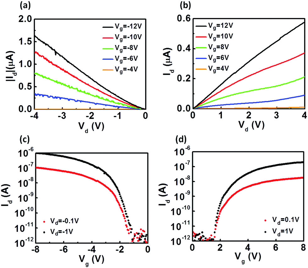 | ||
| Fig. 3 Typical electrical characteristics of the MoS2 fin-shaped field effect transistors. Current versus drain voltage curves at different gate voltages for (a) p-type and (b) n-type operation. Current versus gate voltage curves at different drain voltages for (c) p-type and (d) n-type operation. The p-type behavior is due to the MoS2 film growth from the p+ Si contact while the MoS2 film is an n-type channel as synthesized from the n+ Si contact. | ||
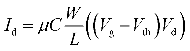
Fig. 4(a) and (b) show the distributions of 20 typical devices’ ON-current (Ion) and threshold voltages (Vth) for n-type and p-type MoS2 fin-FETs in an identical chip. Ion and OFF-current (Ioff) are normalized by the whole channel width (fin circumference) instead of the fin size only. Most of the devices possess a symmetric Vth well while Ion reaches to around 50 μA μm−1 for both n-type and p-type MoS2 fin-FETs with Vd = 1 V. The Ioff for both cases is very low, which is close to 10−5 μA μm−1. The corresponding measured transfer characteristic (Id–Vg) curves for p-type and n-type MoS2 fin-FETs are provided in Fig. S4 and S5 in the ESI.† Note that there are variations in threshold voltage which we think are caused by charges originating from dielectric materials when we deposit HfO2 or Al2O3 on top of MoS2 for the top-gate structure. A comparison of p-type MoS2 performance using our strategy and other methods in the literature is summarized in Table 1.21,23,29,30 The field effect mobility (μ) is extracted from Id–Vg through calculating the approximation equation
 | (1) |
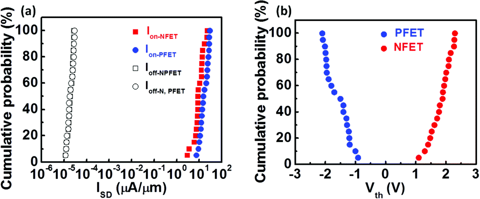 | ||
| Fig. 4 Typical (a) on current (Ion) and off current (Ioff) and (b) threshold voltage (Vth) distribution for 10 n-type and 10 p-type MoS2 fin-shaped field effect transistors in identical chips. | ||
| p-Type silicon [ref. 23] | AlCl3 [ref. 30] | MoOx buffer [ref. 21] | Nb doping [ref. 29] | This work | |
|---|---|---|---|---|---|
| ON-current density (μA μm−1) | 150 | 21 | 0.13 | 1 | 50 |
| ∼500 (effective) | |||||
| ON–OFF ratio | 106 | 107 | 104 | 104 | 106 |
| Mobility (cm2 V−1 s−1) | — | 132 | — | 6.7 | 10 |
| Sample preparation | CVD | Exfoliation | Exfoliation | Exfoliation | CVD |
| Channel structure | Planar | Planar | Planar | Planar | Fin-shaped |
Since a dual gate structure (top and bottom gates) is designed in our MoS2 fin-FETs for better control, the back gate is used to adjust the threshold voltages in both n- and p-type MoS2 fin-FETs. Note that MoS2 on the gate oxide in the fin and planar structure is about 100 nm and 30 nm respectively (see Fig. 1(a) and (c)). The back gate can simultaneously tune both regions in MoS2 to produce a unitary phenomenon. By controlling the back gate bias, we can correct device variations or dynamically configure a device as a high-performance or low energy consumption device in order to achieve higher speed and/or lower power applications. Fig. 5(a) and (b) show the results that back gate voltage can effectively shift the threshold voltages and the comparison of the Vth shift by the back gate for n- and p-type MoS2 fin-FETs is displayed in Fig. 5(c). We can clearly observe from Fig. 5(c) that the threshold voltage is adjustable for the tuning of the 0.5 V shift per back-gate bias applied (0.5 V/1 V) based on the back-gate control. However, the separated back gate for n- and p-type MoS2 fin-FETs is needed to selectively control individual devices in order to achieve adjustable device performance in the future.
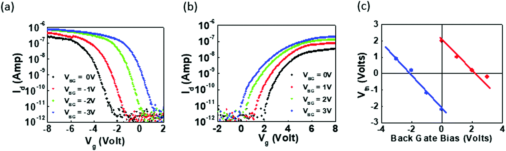 | ||
| Fig. 5 Transfer characteristics for (a) p-type MoS2 fin-shaped field effect transistors and (b) n-type MoS2 fin-shaped field effect transistors under different back gate voltage control. (c) Threshold voltage (Vth) dependence of the back gate bias for p- and n-type MoS2 fin-shaped field effect transistors. | ||
A complementary MoS2 inverter for basic integrated circuit complementary device applications was demonstrated by integrating one n-MoS2 fin-FET and one p-MoS2 fin-FET connected in series without back-gate voltage. The device schematic is shown in Fig. 6(a). The transfer characteristic curves of the CMOS2 inverter as a function of VDD are shown in Fig. 6(b), which exhibits a clear inversion signal with high Vout and low Vin. From the result, it is indicated that the noise margin to get reliable data is VDD larger than 0.1 V. The peak dc voltage gain, |∂Vout/∂Vin|, of the CMOS2 fin-FET inverter is measured to be 20 times larger at a supply voltage VDD of 3 V with a full width at half maximum (FWHM) of 0.15 V, as shown in Fig. 6(c). Compared to hetero material (MoS2/WSe2) based complementary inverters that could achieve a DC gain higher than 100,31 the performance of our inverters still has room for improvement. In the case of complementary inverters constructed by the same doped 2D materials (WSe2/WSe2, MoTe2/MoTe2), our work shows comparable results of the DC gain.32,33 Mostly, the CMOS2 inverter we demonstrated is superior to inverters based on MoS2 reported.34,35Table 2 shows a comparison of the device performance and the material structure between this work and devices made from others.31,36–39
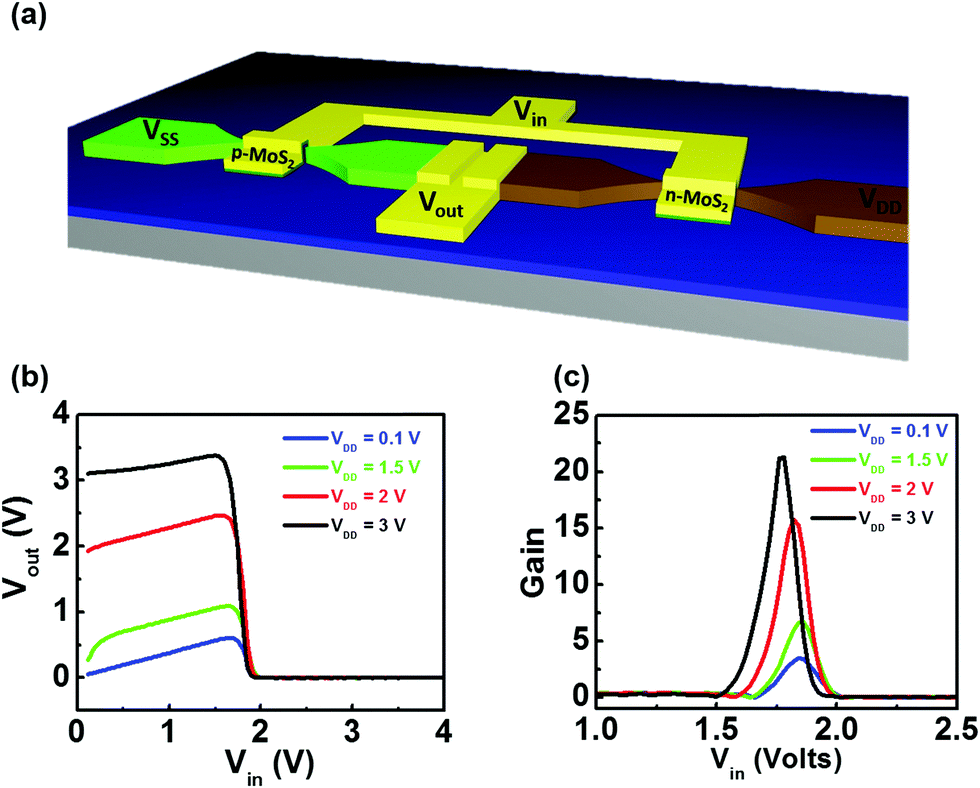 | ||
| Fig. 6 MoS2 fin-shaped field effect transistor inverters. (a) Schematic plot of a MoS2 fin-shaped field effect transistor inverter. (b) Voltage-transfer characteristics of the complementary MoS2 inverters at different VDD. (c) Direct-current voltage gain of the inverter at different supply voltages. | ||
| [Ref. 31] | [Ref. 36] | [Ref. 37] | [Ref. 38] | [Ref. 39] | This work | |
|---|---|---|---|---|---|---|
| DC gain | 110@2 V | 25@5 V | 38@2 V | 13.7@2 V | 60@5 V | 22@3 V |
| 80@2.8 V | 33@3 V | |||||
| Sample preparation | CVD | CVD | Exfoliation | Exfoliation | CVD | CVD |
| Channel materials and structure | Planar MoS2 + WSe2 | Planar WSe2 | Planar WSe2 | Planar MoS2 + WSe2 | Planar MoS2 | Fin-shaped MoS2 |
We have demonstrated the chip-scale growth of continuous layered MoS2 fully covered on an SiO2 fin-shaped structure and integration of n-type and p-type MoS2 by using the traditional implantation technique to exhibit complementary MoS2 fin-shaped field effect transistors. The highly doped n+ and p+ Si as the nucleation seeds to grow MoS2 can induce Fermi level tuning and successfully make MoS2 with n- and p-type operations possible. These MoS2 fin-shaped field effect transistors typically show a few tens μA μm−1 in average ON current and around 106 in current ON/OFF ratio. Accordingly, the complementary MoS2 inverter is displayed with more than 20 high voltage gain. A better understanding to grow MoS2 on higher fin oxide structures or uneven topography is an interesting task to figure out the growth mechanism behind this. The results are fascinating and promising for the future development of full wafer availability in stacked 3D integrated circuit applications based on 2D materials.
Conflicts of interest
The authors declare no conflicting financial interest.Acknowledgements
This work was supported by the National Science Council, Taiwan under contract No. MOST 105-2112-M-003-016-MY3. This work was also in part supported by the National Nano Device Laboratories. Y.-W. Lan, P.-C. Chen, Y.-Y. Lin, Y.-L. Tu and K.-S. Li fabricated the devices and carried out OM, SEM, TEM, Raman measurements and the electrical characterization. M.-Y. Li and L.-J. Li synthesized the 2D materials. Y.-W. Lan, M.-C. Chen, F.-L. Yang and K.-S. Li supervised the study. Y.-W. Lan, M.-C. Chen and K.-S. Li analyzed the data and wrote the paper with significant inputs from all authors. All authors have read and approved the manuscript. All authors discussed the results and commented on the manuscript.References
- G. E. Moore, Cramming more components onto integrated circuits, Electronics, 1965, 38(8), 114–117 Search PubMed.
- J.-P. Colinge, Multiple-gate SOI MOSFETs, Solid-State Electron., 2004, 48, 897–905 CrossRef CAS.
- C. Hu, S. C. Tam, F. C. Hsu, P. K. Ko and T. Y. Chan, Hot-electron induced MOSFET degradation: model, monitor and improvement, IEEE Trans. Electron Devices, 1985, 32, 375–385 Search PubMed.
- S. Ogura, P. J. Tsang, W. W. Walker, D. L. Critchlow and J. F. Shepard, Design and characteristics of the lightly doped drain-source (LDD) insulated gate field-effect transistor, IEEE Trans. Electron Devices ED-27, 1980, 1359–1367 Search PubMed.
- D. Hisamoto, W. C. Lee, J. Kedzierski, T. Hideki, A. Kazuya, C. Kuo, E. Anderson, T. J. King, J. Bokor and C. M. Hu, Fin FET – A Self-Aligned Double-Gate MOSFET Scalable to 20 nm, IEEE Trans. Electron Devices, 2000, 47(12), 2320–2325 CrossRef CAS.
- A. K. Geim and K. S. Novoselov, The rise of graphene, Nat. Mater., 2007, 6, 183–191 CrossRef CAS PubMed.
- B. Radisavljevic, A. Radenovic, J. Brivio, V. Giacometti and A. Kis, Nat. Nanotechnol., 2011, 6, 147 CrossRef CAS PubMed.
- M. S. Choi, G. H. Lee, Y. J. Yu, D. Y. Lee, S. H. Lee, P. Kim, J. Hone and W. J. Yoo, Nat. Commun., 2013, 4, 1624 CrossRef PubMed.
- H. M. Li, D. Y. Lee, M. S. Choi, D. Qu, X. Liu, C. H. Ra and W. J. Yoo, Sci. Rep., 2014, 4, 4041 CrossRef PubMed.
- M. S. Choi, D. Qu, D. Lee, X. Liu, K. Watanabe, T. Taniguchi and W. J. Yoo, ACS Nano, 2014, 8, 9332 CrossRef CAS PubMed.
- B. Radisavljevic, M. B. Whitwick and A. Kis, ACS Nano, 2011, 5, 9934 CrossRef CAS PubMed.
- M. Buscema, M. Barkelid, V. Zwiller, H. S. van der Zant, G. A. Steele and A. Castellanos-Gomez, Nano Lett., 2013, 13, 358 CrossRef CAS PubMed.
- A. Splendiani, et al., Emerging photoluminescence in monolayer MoS2, Nano Lett., 2010, 10, 1271–1275 CrossRef CAS PubMed.
- K. F. Mak, C. Lee, J. Hone, J. Shan and T. F. Heinz, Atomically thin MoS2: A new directgap semiconductor, Phys. Rev. Lett., 2010, 105, 136805 CrossRef PubMed.
- K. He, C. Poole, K. F. Mak and J. Shan, Experimental demonstration of continuous electronic structure tuning via strain in atomically thin MoS2, Nano Lett., 2013, 13, 2931–2936 CrossRef CAS PubMed.
- H. J. Conley, et al., Bandgap engineering of strained monolayer and bilayer MoS2, Nano Lett., 2013, 13, 3626–3630 CrossRef CAS PubMed.
- A. Castellanos-Gomez, et al., Local strain engineering in atomically thin MoS2, Nano Lett., 2013, 13, 5361–5366 CrossRef CAS PubMed.
- P. J. Jeon, J. S. Kim, J. Y. Lim, Y. Cho, A. Pezeshki, H. S. Lee, S. Yu, S. W. Min and S. Im, Low Power Consumption Complementary Inverters with n-MoS2 and p-WSe2 Dichalcogenide Nanosheets on Glass for Logic and Light-Emitting Diode Circuits, ACS Appl. Mater. Interfaces, 2015, 40, 22333–22340 CrossRef PubMed.
- A. B. Sachid, M. Tosun, S. B. Desai, C. Y. Hsu, D. H. Lien, S. R. Madhvapathy, Y. Z. Chen, M. Hettick, J. S. Kang, Y. P. Zeng, J. H. He, E. Y. Chang, Y. L. Chueh, A. Javey and C. M. Hu, Monolithic 3D CMOS Using Layered Semiconductors, Adv. Mater., 2016, 28, 2547–2554 CrossRef CAS PubMed.
- A. Nipane, D. Karmakar, N. Kaushik, S. Karande and S. Lodha, Few-Layer MoS2 p-Type Devices Enabled by Selective Doping Using Low Energy Phosphorus Implantation, ACS Nano, 2016, 10, 2128–2137 CrossRef CAS PubMed.
- S. Chuang, C. Battaglia, A. Azcatl, S. McDonnell, J. S. Kang, X. T. Yin, M. Tosun, R. Kapadia, H. Fang, R. M. Wallace and A. Javey, MoS2 P-type Transistors and Diodes Enabled by High Work Function MoOx Contacts, Nano Lett., 2014, 10, 1337–1342 CrossRef PubMed.
- Y. T. Tang, K. S. Li, L. J. Li, M. Y. Li, C. H. Lin, Y.-J. Chen, C. C. Chen, C. J. Su, B. W. Wu, C. S. Wu, M. C. Chen, J. M. Shieh, W. K. Yeh, P. C. Su, T. Wang, F. L. Yang and C. Hu, A Numerical Study of Si-TMD Contact with n/p Type Operation and Interface Barrier Reduction for Sub-5 nm Monolayer MoS2 FET, IEEE International Electron Devices Meeting (IEDM), 2016, pp. 14.3.1–14.3.4.
- K.-S. Li, B.-W. Wu, L.-J. Li, M.-Y. Li, C.-C. Kevin Cheng, C.-L. Hsu, C.-H. Lin, Y.-J. Chen, C.-C. Chen, C.-T. Wu, M.-C. Chen, J.-M. Shieh, W.-K. Yeh, Y.-L. Chueh, F.-L. Yang and C. Hu, MoS2 U-shape pMOSFET with 10 nm Channel Length and Doped Poly-Si Source/Drain Serving as Seed for Full Wafer CVD MoS2 Availability, IEEE Symposium on VLSI Technology, 2016, pp. 1–2.
- M.-C. Chen, K.-S. Li, L.-J. Li, A.-Y. Lu, M.-Y. Li, Y.-H. Chang, C.-H. Lin, Y.-J. Chen, Y.-F. Hou, C.-C. Chen, B.-W. Wu, C.-S. Wu, I. Yang, Y.-J. Lee, J.-M. Shieh, W.-K. Yeh, J.-H. Shih, P.-C. Su, A. B. Sachid, T. Wang, F.-L. Yang and C. Hu, TMD FinFET with 4 nm Thin Body and Back Gate Control for Future Low Power Technology, IEEE International Electron Devices Meeting (IEDM), Washington, DC, 2015, pp. 32.2.1–32.2.4.
- C. D. English, G. Shine, V. E. Dorgan, K. C. Saraswat and E. Pop, Improved Contacts to MoS2 Transistors by Ultra-High Vacuum Metal Deposition, Nano Lett., 2016, 16, 3824–3830 CrossRef CAS PubMed.
- Y. Guo, Y. Han, J. Li, A. Xiang, X. Wei, S. Gao and Q. Chen, Study on the Resistance Distribution at the Contact between Molybdenum Disulfide and Metals, ACS Nano, 2014, 8(8), 7771–7779 CrossRef CAS PubMed.
- B. W. H. Baugher, H. O. H. Churchill, Y. Yang and P. Jarillo-Herrero, Intrinsic electronic transport properties of high-quality monolayer and bilayer MoS2, Nano Lett., 2013, 13, 4212–4216 CrossRef CAS PubMed.
- R. Kappera, D. Voiry, S. EbruYalcin, B. Branch, G. Gupta, A. D. Mohite and M. Chhowalla, Phase-engineered low-resistance contacts for ultrathin MoS2 transistors, Nat. Mater., 2014, 13, 1128–1134 CrossRef CAS PubMed.
- S. Das, M. Demarteau and A. Roelofs, Nb-doped single crystalline MoS2 field effect transistor, Appl. Phys. Lett., 2015, 106, 173506 CrossRef.
- X. Liu, D. Qu, J. Ryu, F. Ahmed, Z. Yang, D. Lee and W. Jong Yoo, P-Type Polar Transition of Chemically Doped Multilayer MoS2 Transistor, Adv. Mater., 2016, 28, 2345 CrossRef CAS PubMed.
- J. Pu, K. Funahashi, C.-H. Chen, M.-Y. Li, L.-J. Li and T. Takenob, Highly Flexible and High-Performance Complementary Inverters of Large-Area Transition Metal Dichalcogenide Monolayers, Adv. Mater., 2016, 28, 4111 CrossRef CAS PubMed.
- M. Tosun, S. Chuang, H. Fang, A. B. Sachid, M. Hettick, Y. Lin, Y. Zeng and A. Javey, High-Gain Inverters Based on WSe2 Complementary Field-Effect Transistors, ACS Nano, 2014, 8, 4948 CrossRef CAS PubMed.
- J. Yeong Lim, A. Pezeshki, S. Oh, J. Sung Kim, Y. Tack Lee, S. Yu, D. Kyung Hwang, G.-H. Lee, H. Joon Choi and S. Im, Homogeneous 2D MoTe2 p–n Junctions and CMOS Inverters formed by Atomic-Layer-Deposition-Induced Doping, Adv. Mater., 2017, 29, 1701798 CrossRef PubMed.
- B. Radisavljevic, M. B. Whitwick and A. Kis, Integrated Circuits and Logic Operations Based on Single-Layer MoS2, ACS Nano, 2011, 5, 9934 CrossRef CAS PubMed.
- H. Wang, L. Yu, Y.-H. Lee, Y. Shi, A. Hsu, M. L. Chin, L.-J. Li, M. Dubey, J. Kong and T. Palacios, Integrated Circuits Based on Bilayer MoS2 Transistors, Nano Lett., 2012, 12, 4674 CrossRef CAS PubMed.
- S. Das, M. Dubey and A. Roelofs, High gain, low noise, fully complementary logic inverter based on bi-layer WSe2 field effect transistors, Appl. Phys. Lett., 2014, 105, 083511 CrossRef.
- L. Yu, A. Zubair, E. J. G. Santos, X. Zhang, Y. Lin, Y. Zhang and T. Palacios, High-Performance WSe2 Complementary Metal Oxide Semiconductor Technology and Integrated Circuits, Nano Lett., 2015, 15(8), 4928–4934 CrossRef CAS PubMed.
- A.-J. Cho, K. C. Park and J.-Y. Kwon, A high-performance complementary inverter based on transition metal dichalcogenide field-effect transistors, Nanoscale Res. Lett., 2015, 10, 115 CrossRef PubMed.
- S. Wachter, D. K. Polyushkin, O. Bethge and T. Mueller, A microprocessor based on a two-dimensional semiconductor, Nat. Commun., 2017, 8, 14948 CrossRef CAS PubMed.
Footnote |
| † Electronic supplementary information (ESI) available. See DOI: 10.1039/c8nh00419f |
| This journal is © The Royal Society of Chemistry 2019 |