
 Open Access Article
 This Open Access Article is licensed under a Creative Commons Attribution-Non Commercial 3.0 Unported Licence
Enhanced electrochemical biosensor and supercapacitor with 3D porous architectured graphene via salt impregnated inkjet maskless lithography†
John A.
Hondred
 a,
Igor L.
Medintz
b and
Jonathan C.
Claussen
*a
a,
Igor L.
Medintz
b and
Jonathan C.
Claussen
*a
aDepartment of Mechanical Engineering, Iowa State University, Ames, IA 50011, USA. E-mail: jcclauss@iastate.edu; Tel: +515-294-4690
bU.S. Naval Research Laboratory, Center for Biomolecular Science & Engineering, Washington DC, 20375, USA
First published on 31st January 2019
Abstract
Advances in solution-phase graphene patterning has provided a facile route for rapid, low-cost and scalable manufacturing of electrochemical devices, even on flexible substrates. While graphene possesses advantageous electrochemical properties of high surface area and fast heterogenous charge transport, these properties are attributed to the edge planes and defect sites, not the basal plane. Herein, we demonstrate enhancement of the electroactive nature of patterned solution-phase graphene by increasing the porosity and edge planes through the construction of a multidimensional architecture via salt impregnated inkjet maskless lithography (SIIML) and CO2 laser annealing. Various sized macroscale pores (<25 to ∼250 μm) are patterned directly in the graphene surface by incorporating porogens (i.e., salt crystals) in the graphene ink which act as hard templates for pore formation and are later dissolved in water. Subsequently, microsized pores (∼100 nm to 2 μm in width) with edge plane defects are etched in the graphene lattice structure by laser annealing with a CO2 laser, simultaneously improving electrical conductivity by nearly three orders of magnitude (sheet resistance decreases from >10![[thin space (1/6-em)]](https://www.rsc.org/images/entities/char_2009.gif) 000 to ∼50 Ω sq−1). We demonstrate that this multidimensional porous graphene fabrication method can improve electrochemical device performance through design and manufacture of an electrochemical organophosphate biosensor that uses the enzyme acetylcholinesterase for detection. This pesticide biosensor exhibits enhanced sensitivity to acetylthiocholine compared to graphene without macropores (28.3 μA nM−1 to 13.3 μA nM−1) and when inhibited by organophosphate pesticides (paraoxon) has a wide linear range (10 nM to 500 nM), low limit of detection (0.6 nM), and high sensitivity (12.4 nA nM−1). Moreover, this fabrication method is capable of patterning complex geometries [i.e. interdigitated electrodes (IDEs)] even on flexible surfaces as demonstrated by an IDE supercapacitor made of SIIML graphene on a heat sensitive polymer substrate. The supercapacitor demonstrates a high energy density of 0.25 mW h cm−3 at a power density of 0.3 W cm−3. These electrochemical devices demonstrate the benefit of using SIIML and CO2 laser annealing for patterning graphene electrodes with a multidimensional porous surface even on flexible substrates and is therefore a platform technology which could be applied to a variety of different biosensors and other electrochemical devices.
000 to ∼50 Ω sq−1). We demonstrate that this multidimensional porous graphene fabrication method can improve electrochemical device performance through design and manufacture of an electrochemical organophosphate biosensor that uses the enzyme acetylcholinesterase for detection. This pesticide biosensor exhibits enhanced sensitivity to acetylthiocholine compared to graphene without macropores (28.3 μA nM−1 to 13.3 μA nM−1) and when inhibited by organophosphate pesticides (paraoxon) has a wide linear range (10 nM to 500 nM), low limit of detection (0.6 nM), and high sensitivity (12.4 nA nM−1). Moreover, this fabrication method is capable of patterning complex geometries [i.e. interdigitated electrodes (IDEs)] even on flexible surfaces as demonstrated by an IDE supercapacitor made of SIIML graphene on a heat sensitive polymer substrate. The supercapacitor demonstrates a high energy density of 0.25 mW h cm−3 at a power density of 0.3 W cm−3. These electrochemical devices demonstrate the benefit of using SIIML and CO2 laser annealing for patterning graphene electrodes with a multidimensional porous surface even on flexible substrates and is therefore a platform technology which could be applied to a variety of different biosensors and other electrochemical devices.
Conceptual insightsA new manufacturing method called Salt Impregnated Inkjet Maskless Lithography (SIIML) is introduced and shown to enhance the electrochemical activity of patterned solution-phase graphene. Salt crystals mixed into the graphene ink act as hard templates or porogens for the subsequent creation of macroscale pores. After a solvent-based graphene liftoff process defines the printed graphene electrodes, a CO2 laser removes the salt crystals to reveal the pores (100 nm–2 μm) and to increase the electrical conductivity of the graphene (∼50 Ω sq−1). This three-dimensional hierarchy/architecture provides increased edge plane and defects in the graphene, which improves the catalytic activity and capacitance of patterned graphene. This work demonstrates how the patterned graphene can be functionalized to create a highly sensitive pesticide biosensor and high power/energy density electrochemical supercapacitor. While other researchers have also shown that increasing the surface area of graphene can improve electrochemical activity, few researchers have been able to demonstrate a manufacturing method to pattern high surface area graphene; for those who have, the material typically suffers from low conductivity. In addition, these high surface area, conductive graphene circuits could act as a platform technology for batteries, biofuel cells, electrochemical biosensors, and dye-sensitized solar cells as well as flexible and heat sensitive substrates for wearable technology. |
1. Introduction
Graphene has emerged as one of the most attractive electrocatalytic transduction materials due to its extraordinary electrical and thermal conductivity, high mechanical strength, biocompatibility, high carrier capacity/mobility, and potential high surface area.1–3 Specifically, electrodes comprising graphene and graphene derivatives (graphene nanoparticles, reduced graphene oxides, oxidized graphene, functionalized graphene) have demonstrated high electrical conductivity and/or catalytic capability. For example, in the past decade graphene has been used for electrode materials in electrochemical devices such as supercapacitors,4 batteries,5 fuel cells,6 cell electrode stimuli7,8 and sensors.9,10Graphene is typically produced by chemical vapor deposition (CVD) which can yield nearly pristine (defect-free) single or few layer 2D sheets.11 In the context of electrochemistry, these 2D pristine sheets or basal plane geometry exhibit four orders of magnitude lower specific capacitance and seven orders of magnitude lower electron transfer rates than the edges planes or edge defect sites of the graphene.12 Numerous methods have been used to increase the electrochemical surface area (ECSA) of graphene. For example, nanosphere lithography using self-assembly of polystyrene,13 silica,14 or MnO215 nanospheres has been shown to etch nanopores into CVD grown graphene to increase the defect density in the lattice structure (more edge planes) and consequently improved the sensitivity of electrochemical sensors. Others have constructed three-dimensional CVD grown graphene foam out of a nickel scaffold,16 polystyrene colloidal particles as a sacrificial template,17 as well as various other manufacturing methods derived from chemical vapor deposition, hydrothermal methods, and sugar-blowing production.18 While these methods significantly increase the ECSA of the graphene electrode, they often require clean room technology, and/or high temperature fabrication. Such complex fabrication protocols are hence expensive and not amenable to high-throughput manufacturing such as roll-to-roll fabrication.
Solution-phase graphene provides an attractive alternative to costly CVD grown graphene as it can be synthesized from low-cost graphite with mechanical/chemical exfoliation.19,20 Various methods have been exploited to increase the ECSA of solution-phase graphene. For example, the “breath-figure” method uses moist gas that condenses on organic solution-phase graphene which results in the formation of highly controlled evaporated water droplet pores (∼2 μm).21,22 Others have electrochemically reduced graphene oxide which provides a simple, one-step procedure to create 3D porous graphene coatings with pores ranging between 1–10 μm between graphene flakes.16 Colloidal nanoparticles were used as template scaffolding which produced a hollow free-standing 3D graphene structure (500 nm).23 While each of these methods provide effective means for creating a highly porous 3D graphene architecture, they do not provide facile routes to pattern the solution-phase graphene into electrodes and in many cases are not stable (i.e., the architectures collapse in the air).16
Simple, low-cost methods such as inkjet,24 aerosol,25 and screen printing26 provide simple fabrication methods for patterning solution-phase graphene into highly defined graphene electrodes; however, these graphene surfaces typically have little ECSA as graphene flakes are tightly compact exposing predominately their basal planes.27 Various techniques have been employed to alter the graphene flake orientation, for example, Choi et al., incorporated nafion polymers into the graphene solution which made a hydrophobic (contact angle ∼161°) rough surface, however, the graphene film lacked conductivity (>10 kΩ sq−1).28 Hersam and coworkers used polymer-phase inversion to tailor the porosity of graphene, similarly, the increase in porosity lead to a decrease in conductivity (∼1000 S m−1 at 15% glycerol).29 Alternatively, we have demonstrated that secondary post-processing methods such as laser annealing can significantly increase the conductivity (∼100 Ω sq−1)10 while simultaneously enhancing the electroactive surface area of graphene by nano/micro structuring pores into the graphene by orientating superficial graphene flakes vertically.10,30,31 However, these methods do not make macrosized pores in the graphene surface or micropores in the graphene lattice structure while retaining electrical conductivity. Macropores in the graphene surface facilitate enhanced diffusion of substrates towards and away from the active sites (defect sites and edge planes in the graphene). Therefore, adding the additional three-dimensional hierarchy/architects of different pore sizes, as exhibited in these developed electrodes for example, has been shown to result in higher electroactive surface area and enhanced catalytic activity.32,33
Herein we demonstrate a facile manufacturing process of patterning solution-phase graphene electrodes with high electroactive surface area utilizing different orders of pore sizes via salt impregnated inkjet maskless lithography (SIIML) and CO2 laser annealing. This technique modifies the newly developed IML method for rapid prototyping highly defined graphene films by incorporating salt crystals as porogens to increase the ECSA.10,31 Sieved salt powders have been demonstrated in the past to act as efficient porogens for 3D printed resins,34–36 polymer-nanotube scaffolds for bone formation37 and porous carbon powders for gas absorbance.38 Similarly, we demonstrate that salt crystals can act as a hard template porogens for macrosize (<25 to ∼250 μm) defects in 2D thin film electrochemical devices. We also demonstrate for the first time, the use of a CO2 laser to anneal patterned solution-phased graphene which etches microsize (∼100 nm–2 μm) pores in the graphene surface. This high ECSA graphene surface displayed enhanced electrochemical performance as demonstrated by an electrochemical pesticide biosensor with high sensitivity (12.4 nA nM−1) and low limit of detection (0.6 nM) to paraoxon (a model organophosphate pesticide). Furthermore, we show that this multidimensional porous graphene surface is a platform technology that can be applied to electrochemical devices beyond biosensors, including energy storage, as demonstrated by an electrochemical supercapacitor fabricated via the SIIML process which portrays high energy and power density (0.25 mW h cm−3 at 0.3 W cm−3).
2. Methods and materials
2.1. Chemicals and reagents
Completely chemically reduced single layer graphene oxide (referred to henceforth as graphene) was purchased from ACS Materials (GN1P0005). Sodium chloride (NaCl) was purchased from Sigma-Aldrich, ground using mortar and pestle, and filtered into different sizes with 8 in wire cloth sieves. Acetylcholinesterase (ACHE) from Electrophorus electricus was purchased from Sigma Aldrich as lyophilized powder (200–1000 units per mg) and was used without any further purification. ACHE ink aliquots were made by dissolving the enzyme (2 mg) in 1 mL of 50% glycerol and 50% 1x phosphate–buffer solution (0.1 M PBS, pH 7.0), aliquoted into 25 μL, and stored in a −80 °C freezer until use. All pesticides (including paraoxon) were obtained from Chem Service. All other chemicals and solvents were purchased from Sigma-Aldrich and were used without any other purification unless otherwise stated. Water was filtered through a B-Pure Water Purification system (resistivity, 18.2 MΩ cm−2).2.2. Electrode fabrication
2.3 Biosensor design and fabrication
2.4 Supercapacitor design and fabrication
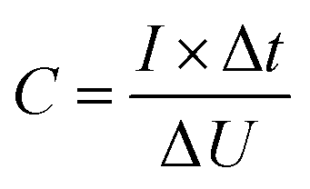 | (1) |
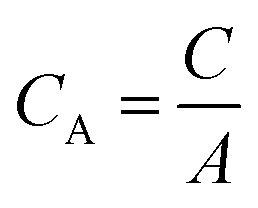 | (2) |
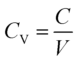 | (3) |
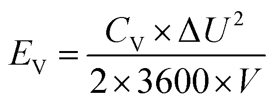 | (4) |
 | (5) |
2.5 Electrochemical surface area (ECSA) calculations
All ECSA experiments were conducted in 5 mM ferri/ferrocyanide in 1x PBS. CVs were conducted with three different scan rates (25, 50, and 100 mV s−1) and were used to calculate the ECSA using the Randle–Sevcik equation (eqn (6)),42,43 refer to representative graphs, Fig. S4 (ESI†).| Ip = 2.69 × 10⁵AD1/2n3/2v1/2C | (6) |
2.6 Field emission SEM images
Field emissions scanning electron microscopy (FESEM) images were acquired using a FEI Quanta 250 FESEM. All images were magnified to 500×, 1500×, 5000×, or 15000× using backscattering electrons, spot size of 3.0, and with a 10 kV potential. A 2 nm conductive coating of iridium was evenly coated over all samples with a turbo-pump sputter coater to improve surface imaging by preventing surface charging and hinders electrons from penetrating into the carbon material leading to poor surface contrast.
3. Results and discussion
3.1 Biosensor Design and Optimization
First, a polymer sacrificial layer is inkjet printed onto a disposable, low-cost, and flexible substrate (PET), Fig. 1a. A highly concentrated graphene ink is then spin-coated over the entire polymer sacrificial layer, followed by an additional graphene ink layer impregnated with salt crystals. The entire sample is then post-baked with a heat-gun to remove solvents and increase graphene adhesion to the substrates, Fig. 1b. As the salt crystals are ionic solids, they do not ionize in the non-polar organic solvent and when patterned form a hard template (porogen) for macrosized pores. The entire graphene surface is then impinged by an acetone wash bottle which removes the underlying polymer sacrificial layer, patterning a highly-defined graphene electrode, Fig. 1c and Movie S1 (ESI†). As acetone is not highly polar, the salt remains in its crystalline form as a hard template beneath the graphene surface. The graphene is then treated with a CO2 laser which anneals the surface, removes remaining solvents, carbonizes surfactants, and “welds” graphene flakes together.9 The CO2 laser also etches micropores into the graphene surface enhancing electrochemical activity by producing additional edge planes in the graphene surface. Furthermore, laser annealing also etches the graphene surface revealing the salt crystals, opening the surface for pore formation, Fig. 1d and Fig. S1 (ESI†). Finally, the electrode is rinsed with DI water which removes the salt porogen crystals, forming macrostructured pores in the graphene surface, Fig. 1e and Movie S2 (ESI†). These macropores improve electrochemical sensing by providing increased analyte diffusion rates and increased ECSA.
 | ||
| Fig. 1 Schematic diagram depicting the fabrication process steps of SIIML graphene electrodes. (a) A sacrificial polymer layer is inkjet printed as the negative of the final pattern. (b) Concentrated graphene ink impregnated with salt crystals is spin-coated. (c) The entire surface is impinged with acetone to remove the sacrificial layer, patterning the graphene. (d) A CO2 laser anneals the graphene which increases conductivity, etches micropores, and reveals the salt crystals. (e) Electrodes are finally rinsed with water to remove the salt porogen, making macrosized pores within the graphene surface. | ||
 | ||
| Fig. 2 Schematic diagram of ACHE biosensor depicting the functionalization strategy for pesticide biosensing using EDC/NHS. (a) From left to right: EDC reacts with carboxyl groups to make an O-acylisourea intermediate ester. NHS reacts to form a stable amine-reactive ester. Finally, NHS ester binds ACHE to graphene surface through available amines in the enzyme. (b) Basic operations of ACHE pesticide biosensor. From top to bottom: ACTH reacts with ACHE and produces acetic acid and thiocholine. Thiocholine (2×) is oxidized by the graphene electrode and produces dithiocholine and two electrons. Paraoxon (model pesticide/organophosphate) inhibits ACHE and prevents the catalysis of ACTH. Note: size not to scale. | ||
This immobilization strategy (EDC/NHS) was chosen as it has been widely studied, covalently crosslinks with “zero order” length to carboxylic functional groups, is water soluble (no prior organic solvent dissolution necessary) and provides excellent subsequent stability to enzymes.46 First, EDC reacts with carboxyl groups (formed through laser annealing) to make an O-acylisourea intermediate ester. Second, to increase stability of this short-lived ester, NHS is added to form a stable amine-reactive NHS ester, which increases immobilization efficiency of EDC coupling reaction.47 Finally, ACHE is then bound to the ester by a free amine in the enzyme, Fig. 2a.
The use of ACHE for inhibited pesticide biosensing has been demonstrated many times in the literature, but for clarity, Fig. 2b illustrates its basic mechanism. The biosensor operates by hydrolyzing the molecule ACTH which produces acetic acid and thiocholine. Two thiocholine molecules are oxidized at the graphene surface at an applied potential of 400 mV, Fig. S5 (ESI†); this reaction produces dithiocholine and two electrons. The thiocholine oxidation reaction is used as a baseline amperometric signal for sensing the inhibition of ACHE by pesticides. As increasing concentrations of pesticides are added to the solution, more ACHE is inhibited which prevents the formation of thiocholine, consequently this reduces the oxidation and amperometric current (see representative amperometric graphs in Fig. S3, ESI†).
000 Ω sq−1 to ∼50 Ω sq−1) (Fig. 3a (blue)). We further confirm the carbonizing of the surfactants by XPS which shows a decrease in the sp3 peak (green) which we attribute to ethyl/nitrocellulose, Fig. 3b. Interestingly, unlike the diode laser or the Nd:YAG,9,10,31 the CO2 laser does not alter the graphene flake orientation; rather, it fuses graphene flakes together (5 W till 5.8 W) increasing the conductivity (∼10 kΩ sq−1 to ∼50 Ω sq−1, Fig. 3a (blue)), then etches through the surface making microsize pores (Fig. 3c). The surface roughness (electrochemical surface area/geometric surface area) of the laser annealed graphene begins to increase (Fig. 3a (red)) as the resistance of the electrode decreases. The not annealed patterned graphene initially has a negligible surface roughness and high electrical resistance. When laser annealing at a power of 5.2 W the graphene surface roughness increased to 2.2. However, as the laser power increased past 5.2 W the graphene flakes begin to “weld” together making a flat plane which decreases the ECSA (surface roughness of 1.7 at 5.6 W) due to decreases in available edge planes. Further increasing the laser power not only “welds” the graphene flakes together promoting even higher conductivity but starts to etch through the basal planes of the graphene which leads to increased edge plane defects by making microsize pores (100 nm–2 μm) in the graphene surface and consequently increasing the electrochemical surface roughness (2.6 at a power of 6.2 W). The conductivity and surface area both decrease after 6.2 W as the graphene is etched through the surface and the substrate begins to degrade. Therefore, for all further experiments the CO2 laser was set to 6.2 W with a 350 mm s−1 raster rate.
 | ||
| Fig. 3 Effects of CO2 laser annealing graphene. (a) Electrode sheet resistance (blue) and electrochemical surface roughness (red) versus increasing laser power. (b) XPS of not annealed, 5.8 W, and 6.4 W laser annealed graphene. (c) Representative SEM of laser annealed graphene surfaces with various powers showing the initial welding of graphene flakes at low power and then etching through the surface making microsized pores at higher powers. | ||
Raman spectroscopy was employed to analyze the atomic structure of the printed graphene and the effect of CO2 laser annealing. Fig. S6 (ESI†) displays the Raman spectra collected from not annealed and increasing laser power annealed graphene (5.2–6.4 W) with a backscattering geometry, 1064 nm Nd:YAG laser and spot size of 1 mm. Note that the spectra has been standardized so all samples have consistent G peak heights. The not annealed printed graphene displayed distinct D and G peaks which are characteristic for graphene and graphitic samples. However, the sharp 2D peak, typically associated with graphene is not visible. The loss of the 2D peak is probably due to the high concentration of surfactants within the printed graphene sample and possible impurities/functional groups on the graphene surface. However, as the laser power increases from 5.2 W to 6.2 W the 2D peak develops, indicating the formation of a graphene like structure by energetic photon irradiation. Furthermore, as the laser intensity increases, there is a decrease in (ID/IG) ratio (from 0.72 for not annealed graphene to 0.17 for 6.2 W) which suggests that the printed graphene forms a higher degree in edge-induced defects, which are conducive towards enhanced electrochemical reactivity.9,49 Additionally as the laser power increases there is an increase in (I2D/IG) ratio (from 0.23 for not annealed graphene to 0.78 for annealed graphene with a laser power of 6.2 W) which correlates with reported multilayer graphene structures.50 At a laser power of 6.4 W, the ratios reverse as the samples are etching through the surface and there are possible formation of van der Waals bonds into more a graphitic nature. In summary, the emergence of a symmetric 2D peak with an increase in (IG/ID) and (I2D/IG) ratio at higher laser powers demonstrates the carbon surface is more nanostructured or nanotextured with a higher amount of edge defects and the sp2 honeycomb lattice of the surface becomes more favorable to classification as multilayered graphene.
It is interesting that we do not see a significant increase in graphene oxidation (Fig. 3b) as we are laser annealing in ambient oxygen atmosphere as seen by our previous work with a diode laser.31 Instead there is approximately a consistent small oxide layer formed across all laser powers. These oxide functional groups are most likely superficial as oxidizing deep into the graphene electrode would decrease the electrode conductivity (not seen in Fig. 3a), which may partially explain the lower sheet resistance of CO2 laser annealing (∼50 Ω sq−1) compared to using a diode laser (∼100 Ω sq−1).10 In any case, the oxidation groups and defects in the graphene surface provides effective functionalization locations for both biomolecules or even nanoparticle nucleation locations, as we have shown previously.9,10,31
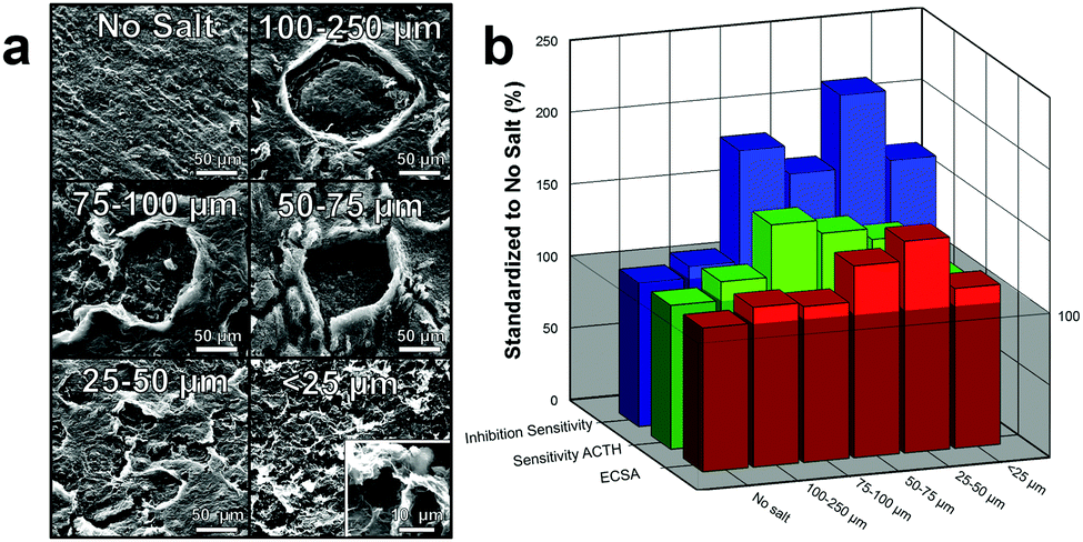 | ||
| Fig. 4 Effects of various size salt crystals for macroscale pore formation. (a) SEM depicting various size salt pores made with decreasing size salt crystals. Bottom right: Magnification of <25 μm pore. (b) Graph demonstrated the effects of different size salt crystals to ECSA (red), sensitivity to 5 mM ACTH (green), and inhibition sensitivity due to 1 μM paraoxon (blue). Note: graph has been standardized to no salt pores for comparison. | ||
This tighter pore array as well as the increased “surface-to-volume” effect (smaller pores will have higher surface area per vacancy ratio) results in an increase in surface area as the size of the pores decrease, Fig. 4b (red). This effect is clearly seen by an over 50% increase in ECSA of electrodes made with 25–50 μm pores compared to electrodes made without salt pores. Interesting, after the pore size decrease below 25 μm, there is a significant decrease in ECSA. While it is not completely understood, we speculate that the size is approaching the microporous size made by laser annealing and is therefore mitigating the effect of one or the other. Additionally, this decrease in ECSA could be from the decrease in perpendicular diffusion of substrate into the electrode which would decrease the electroactivity of the substrate.
Increasing the ECSA of the graphene by incorporating pores significantly enhanced the electroactivity of the electrode by providing additional sites for oxidation or reduction of the substrate.9 Moreover, the higher surface area of the porous graphene also provides additional binding locations for enzymes immobilization, which allow for improved substrate diffusion kinetics and consequently enhanced catalysis.10 Both of these effects improve the performance of the biosensor which increases its sensitivity to the analyte of interest. To test this, the electrodes were placed in a concentrated solution (5 mM) of ACTH with a working potential of 400 mV (versus Ag/AgCl). When ACTH reacts with ACHE, thiocholine is produced which oxidizes at the electrode. The corresponding increase in current due to the sensitivity to ACTH was graphed, Fig. 4b (green). As the size of the pores decrease and the ECSA increases, there is a general increase in sensitivity to ACTH as expected. Variations from this trend (150% for 75–100 μm and 133% for 25–50 μm), are likely due to manufacturing errors (enzyme loading differences), experimental setup (sensors did not full equalize to baseline), or random/systematic errors. These results are further demonstrated by SIIML graphene biosensor with 25–50 μm being over 2 times more sensitive to the ACHE than without salt pores, Fig. 4b (blue). For all further experiments, 25–50 μm salt particles were used as they exhibited the highest ECSA and was the most sensitive to paraoxon.
The concentration of the 25–50 μm salt/graphene ink suspension was varied to improve the pore array density of the graphene surface, Fig. 5a. As the salt concentration increased, the pores in the graphene surface on average come closer together forming a denser pore array. At 50 mg mL−1, the pores are fairly far apart, and a sparse array is formed (roughly estimated by visibly counting pores in SEM, ∼75–125 pores per cm). When the concentration was increased to 250 mg mL−1 a network of pores are formed (∼300–500 pores per cm), and at 500 mg mL−1 a very dense array of pores is present (∼500–750 pores per cm). Note that as the concentration of salt increases and the salt packs closer together, the pore structures are harder to distinguish due to overlap. Additionally, as the salt concentration increases, the viscosity of the graphene ink also increases. At 500 mg mL−1, the ink is much more viscous (making it more difficult to spin-coat) and so a thicker layer of graphene may have been applied which results in the salt not all lying flat against the bottom surface causing salt porogen overlap, Fig. S7 (ESI†).
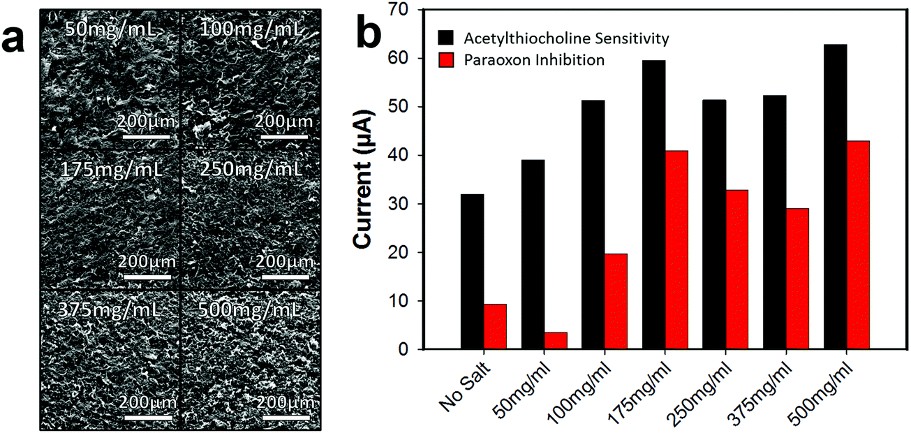 | ||
| Fig. 5 Effects of various salt concretions in graphene ink. (a) Representative SEM depicting concentrations of salt forming sparse to dense pore arrays in the graphene. (b) Graph demonstrated the effects of different concentrations of salt for sensitivity to 5 mM ACHE (Black), and inhibition sensitivity due to 1 mM paraoxon (Red). | ||
As the pore structure in the graphene becomes denser, the biosensor electrode (functionalized with ACHE), becomes more sensitive to ACTH (Fig. 5b), however, it appears that after 175 mg mL−1, the anodic current relatively plateaus. Interesting, this trend is not completely observed with the inhibition sensitivity of paraoxon and after 175 mg mL−1 the sensitivity begins to decrease. This observation is not easily explained, but we speculate that the higher surface area increased the loading of the enzyme on the graphene, resulting in more enzyme that needed to be inhibited. As the concentration of 175 mg mL−1 yielded a porous graphene biosensor with the most sensitivity to ACTH and the signal response was most inhibited by paraoxon, all further experiments were conducted with this salt concentration.
3.2 Biosensor performance characterization
The electrochemical activity of SIIML graphene electrodes was demonstrated by manufacturing a pesticide biosensor using ACHE and refined parameters shown previously (6.2 W CO2 laser annealing, 50–75 μm salt pores, and 175 mg mL−1 salt concentration). First, an array (4 × 10) of 3 mm diameter disk electrodes were manufactured using the procedure outlined in the Overview SIIML Graphene Electrode Fabrication (Fig. 6a). A lacquer was then pipetted onto the stem of the electrode to isolate the working area (3 mm diameter disk) and biofunctionalization was carried out as described in the Overview Pesticide Biosensor Fabrication. The ACHE pesticide sensor was placed in a saturated solution (5 mM) of ACTH and amperometric current was recorded with changing potentials (Fig. 6b). When the potential reached 200 mV (versus Ag/AgCl) there was an increase in anodic current due to the oxidation of thiocholine. This oxidation current increases as the applied potential approaches 400 mV then plateaus, therefore, an applied potential of 400 mV was chosen for the ACHE biosensor. This observation is in good agreement with CV scans that show an oxidation peak around 400 mV (Fig. S5, ESI†) and similarly reported in the literature.51,52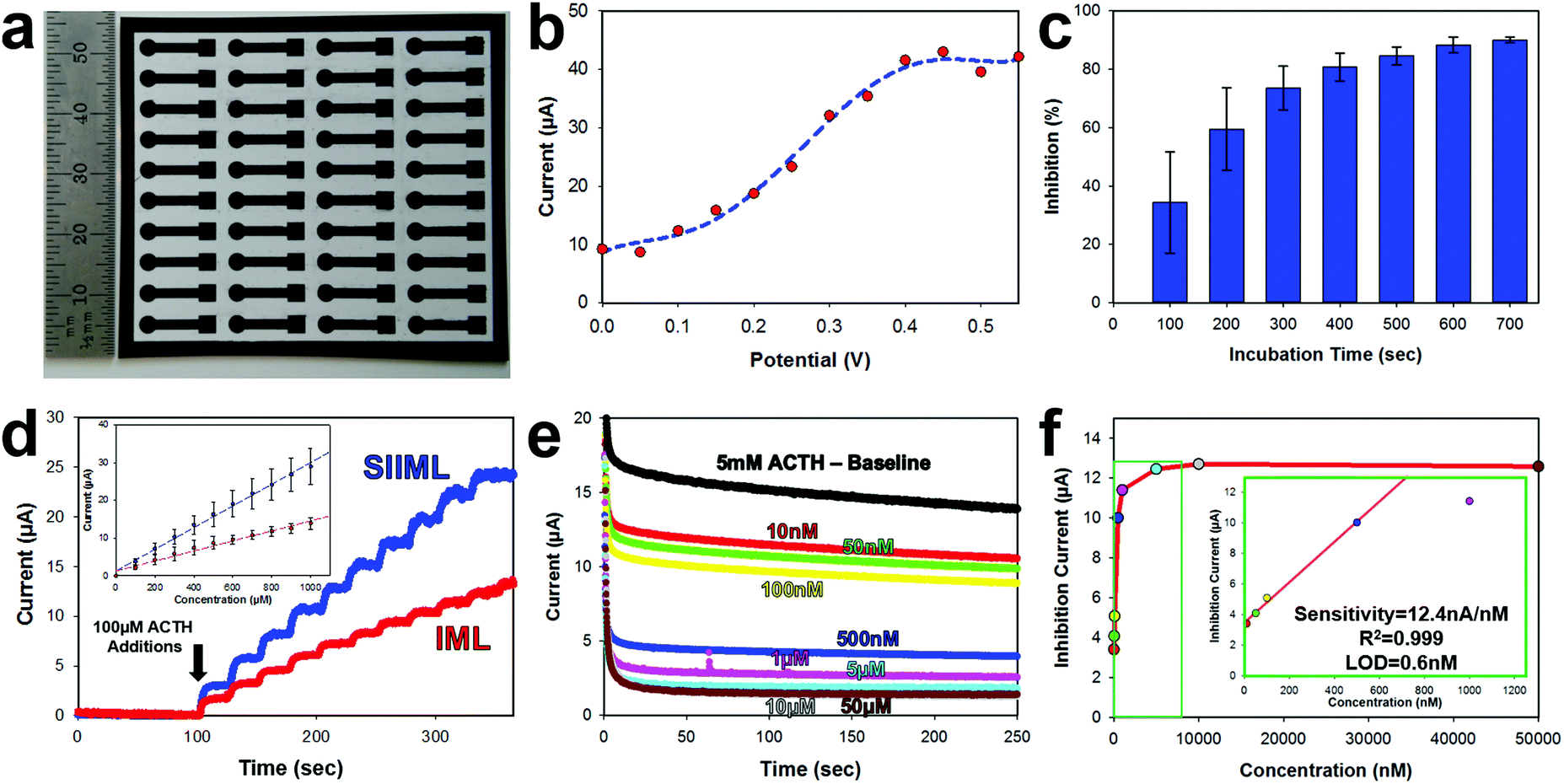 | ||
| Fig. 6 ACHE pesticide biosensor characterization. (a) Photograph of patterned array (4 × 10) SIIML graphene electrodes on flexible PET substrate. (b) Effect of applied potential to amperometric response of 1 mM ACTH. (c) Plot of inhibition (%) according to incubation time. (d) Sensitivity to ACTH for SIIML (blue) and IML (red), inset: current versus concentration. (e) Amperograms of pesticide ACHE biosensor after incubating with various concentrations of paraoxon. Buffer baseline (black), 10 nM (red), 50 nM (green), 100 nM (yellow), 500 nM (blue), 1 μM (pink), 5 μM (aqua blue), 10 μM (grey), 50 μM (brown). (f) Corresponding current versus concentration, inset: magnification showing linear sensing range. | ||
ACHE pesticide biosensors rely on the inhibition of the enzyme (paraoxon irreversibly binds to ACHE which prevents ACTH from catalyzing and hence thiocholine from oxidizing). Therefore, to test the amount of time required for organophosphates to diffuse to the electrode surface and bind to ACHE, we incubated the sensors in 1 μM of paraoxon and recorded the decrease in amperometric oxidation current (which correlates directly with the percent of ACHE inhibited), Fig. 6c. After 100 seconds, there is roughly 50% inhibition of the sensor with large standard deviations; however, after 500 seconds, there is about 90% inhibition with low standard deviation and minimal change over the next couple of hundred seconds. Therefore, an incubation time of 500 seconds was used as a minimal time for sensor operation.
Graphene electrodes were made with (SIIML) and without salt pores (IML) for comparison. Increasing concentrations of ACTH (100 μM additions) were spiked into a buffer solution and the amperometric anodic current was recorded for both SIIML and IML. The electrodes containing salt pores had a sensitivity to ACTH of 28.3 μA nM−1 while the electrodes without salt pores had a sensitivity of ∼13.3 μA nM−1, Fig. 6d.
Finally, the SIIML were tested for pesticide sensing with paraoxon (a model organophosphate pesticide). It should be noted here that a diluted concentration of ACHE was applied to these pesticide biosensors (∼2 U per sensor) as having a smaller concentration of enzyme results in higher sensitivity due to less enzyme that needs to be inhibited.40 An amperometric baseline of eight different SIIML ACHE pesticide biosensors were recorded in 5 mM ACTH which had an anodic current of 13.84 ± 0.3 μA. Each of the sensors were then placed in different concentrations of paraoxon (10 nM–50 μM) and incubated for a minimum of 5 min, and then placed back in the same 5 mM ACTH solution (Fig. 6e). The concentration versus inhibition current (decrease in anodic current) was graphed (Fig. 6f) and showed a linear region up to 500 nM and then a plateau region shortly thereafter. The sensitivity of the linear region was calculated to be 12.4 nA nM−1 with a limit of detection of 0.6 nM (LOD = 3 noise per signal, noise defined as standard deviation of three electrodes without ACHE). Therefore, our sensor has a limit of detection below the tolerable drinking water equivalence level of the United States and Canada EPA (24 nM and 170 nM, respectively).53,54 There are many reported ACHE biosensors with lower limit of detection, even as low as 0.4 pM;55 however, these biosensors often employ complex methods to enhance their sensitivity and reduce noise such as metal nanoparticles,56,57 multilayer carbon nanotube-modified glassy carbon electrodes,55 co-enzymes,58 flow cells55,59 or microelectrodes.60
3.3 Supercapacitor performance characterization
To further demonstrate the enhanced electrochemical activity of SIIML electrodes, supercapacitors were designed. Supercapacitors offer promising energy storage opportunities for on-chip devices as they can be fabricated directly in line with the electronics.61 Supercapacitors store energy at the interface of the electrode and electrolyte; therefore, increasing the ECSA and conductivity of the electrode improves the efficiency and capacitance of the supercapacitor.62 Interdigitated electrodes (IDEs) were designed and patterned using the procedures outlined in the Overview SIIML Graphene Electrode Fabrication, and an array (2 × 4) of IDEs were patterned, Fig. 7a. The SIIML graphene IDEs were then coated with PVA/H3PO4 gel which acts as a dry gel electrolyte. The performance of the SIIML graphene supercapacitor was first examined with CVs of various scan rates (50 mV s−1 – black to 1000 mV s−1 – orange), Fig. 7b. The CVs show a rectangular shape at low scan rates and only begin to distort in shape at very high scan rates (1000 mV s−1) due to internal resistance. The capacitive current (due to double layer charging) of the SIIML graphene electrodes was extracted from the CVs and compared with IML graphene with no salt. The graphene with salt pores displayed enhanced double layer capacitance (37%) current as portrayed in Fig. 7c. Galvanostatic charge–discharge profiles of the SIIML were then graphed which shows relatively symmetric triangular shape, but slowly loses symmetry at very low charging densities (0.01 mA cm−2). Based on the discharge rates, the capacitance was calculated and graphed versus the current density, Fig. S8 (ESI†). On average, the SIIML graphene had ∼30% more capacitance than the devices without salt (IML).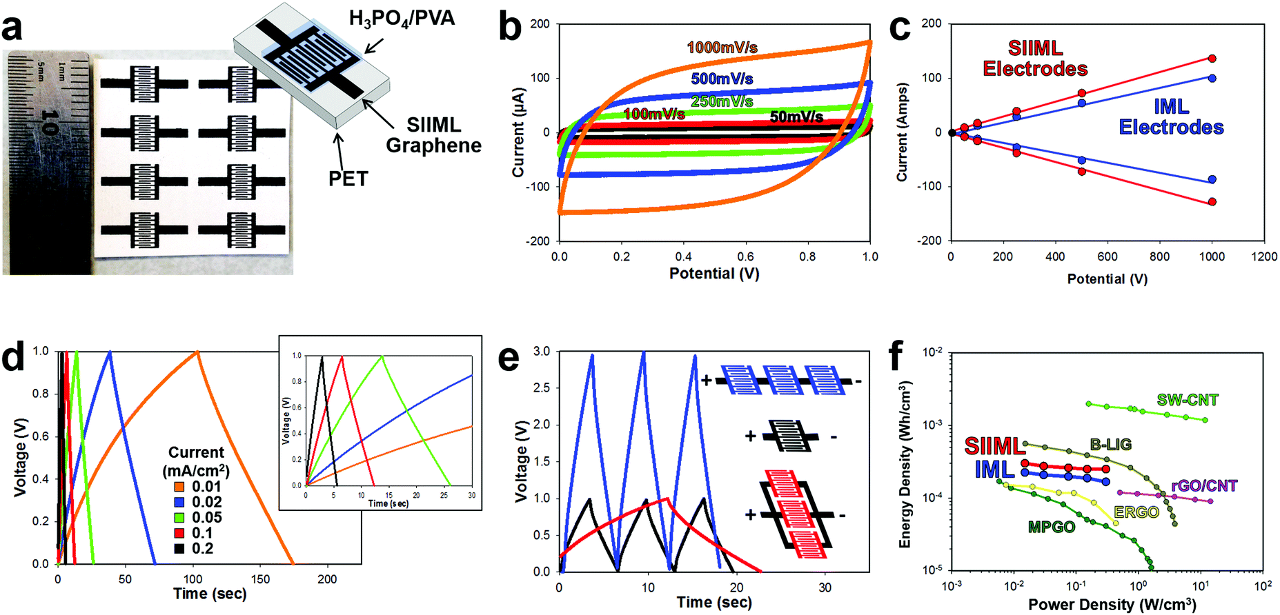 | ||
| Fig. 7 Electrochemical performance of a SIIML supercapacitor. (a) Photograph of patterned SIIML graphene electrode with schematic of supercapacitor design. (b) Cyclical voltammograms with increasing scan rates (50 mV s−1 black to 1000 mV s−1 orange). (c) Scan rate versus current demonstrating linear relationship and enhanced capacitance of SIIML (red) over IML (blue). (d) Galvanostatic charge–discharge curves with different current densities (0.01 mA cm−2 − orange to 0.2 mA cm−2 – red), inset: magnification showing near triangular shapes at higher current densities. (e) Galvanostatic charge–discharge graph of single supercapacitor (black), three electrodes connected in series (blue), and three electrodes connected in parallel (red). (f) Ragone plot of SIIML (red) and IML (blue) supercapacitor electrodes and various other carbon-based IDE supercapacitors; light green: inkjet printed single walled carbon nanotubes (SW-CNT),63 brown: boron doped laser induced graphene (B-LIG),69 pink: electrostatic spray deposited reduced graphene oxide/carbon nanotube (rGO/CNT),70 yellow: electrochemically reduced graphene oxide (ERGO),71 and dark green: methane plasma treated graphene oxide with gold collector (MPGO).72 | ||
Multiple supercapacitors can be connected in series (to boost voltage capabilities) or in parallel (to increase energy storage density) as illustrated and graphed in Fig. 7e. When three electrodes are connected in series (blue) the voltage window increased by a factor of three with roughly the same charge–discharge times. In contrast, when three electrodes are connected in parallel, the charge–discharge times increase by a factor of three with the voltage window remaining constant. Therefore, these supercapacitors could easily be patterned in series or parallel to adapt for a specific application. To demonstrate that SIIML graphene patterning process for supercapacitor use, an array of supercapacitors were fabricated (3 in series and 5 in parallel) and were used to power a red LED (drop voltage ∼1.8 V). After charging the supercapacitor to 3 V, the LED was tested across the supercapacitor array and illuminated multiple times before the supercapacitor's voltage decreased below 1.8 V, see Movie S3 (ESI†).
Finally, the SIIML graphene and IML graphene (no salt) energy density and power density were extracted from the galvanostatic discharge and graphed on a Ragone plot (Fig. 7f).63,64 The graphene electrodes that contained salt pores demonstrated higher energy density due to the increase in ECSA which stored more charge at the graphene/electrolyte interface. Both the SIIML and the IML graphene interdigitated electrodes compared favorably with other carbon-based supercapacitors IDEs reported in the literature, with the SIIML outperforming the IML electrode (energy density of 0.25 mW h cm−3 and 0.17 W h cm−3 at a power density of 0.3 W cm−3, respectively). Note that supercapacitors are strongly dependent on the electrolyte used, and by using a more efficient electrolyte, a higher energy and power density could be obtained.65–68
4. Conclusions
In conclusion, a micromanufacturing technique for enhancing the electrocatalytic activity of patterned solution-phase graphene was demonstrated with the use of a modified IML technique. This technique creates a multiscale porous architecture in the graphene surface. Macrosized pores (25–50 μm) are formed by utilizing salt crystals as porogens (hard templates) in the graphene ink while patterning, referred to as salt impregnated inkjet maskless lithography (SIIML). Additionally, microsized pores (100 nm–2 μm) are etched into the graphene surface through CO2 laser annealing, even on flexible heat sensitive substrates (PET). We demonstrate that SIIML is an effective tool for enhancing the electrochemical activity of graphene by fabrication of an electrochemical pesticide biosensor, which utilizes ACHE. Graphene electrodes with macrosized pores through salt impregnation outperformed their non macropore counterparts (sensitivity to ACTH of 28.3 μA nM−1 to 13.3 μA nM−1). The final SIIML graphene ACHE sensor had a wide linear sensing range (10 nM to 500 nM), low limit of detection (0.6 nM), and high sensitivity (12.4 nA nM−1) to paraoxon which is below the tolerable drinking limit reported by the EPA.53 Furthermore, we demonstrate that this method can fabricated complex geometries such as interdigitated electrodes for use in other non-biosensing related applications (i.e., an electrochemical supercapacitor). Critically, the SIIML graphene outperformed non-macroporous graphene by demonstrating ∼30% higher capacitance. The SIIML supercapacitor demonstrated excellent energy density of 0.25 mW h cm−3 at a power density of 0.3 W cm−3, which was comparable to other carbon-based supercapacitors reported in literature. Both the electrochemical biosensor and supercapacitor demonstrate that increasing the electrochemical surface area of solution-phase printed graphene electrodes via SIIML and CO2 laser annealing improves the performance of these electrochemical devices. Moreover, these manufacture techniques (SIIML and CO2 laser annealing) are amenable to thermally sensitive and flexible substrate materials; therefore, this method could be adapted to wearable technology for energy storage or textile-based biosensors5,73–75 as well as for potential creation of flexible supercapacitors on paper-based substrates.76 Finally, this high ECSA graphene transduction electrode can act as a platform technology for additional electrochemical sensors or supercapacitors, as well other electrochemical devices such as batteries,77 biofuel cells,78 dye sensitive solar cells,79 or electrode stimuli.8,48Conflicts of interest
The authors declare no competing financial interest.Acknowledgements
J. C. C. gratefully acknowledges funding support for this work by the National Institute of Food and Agriculture, U.S. Department of Agriculture, under award number 2018-67011-27989 and 2016-67021-25038, from the National Science Foundation under award number CBET-1706994 and ECCS-1841649, and the Roy J. Carver Trust under award number 15-4615. I. L. M. acknowledges ONR and NRL for Funding Support. Special thanks is given to Steven Kmiec and Steve Martin of Materials Science and Engineering (MSE) of Iowa State University for providing Raman Spectra.References
- R. Raccichini, A. Varzi, S. Passerini and B. Scrosati, Nat. Mater., 2015, 14, 271 CrossRef CAS PubMed.
- S. L. Burrs, M. Bhargava, R. Sidhu, J. Kiernan-Lewis, C. Gomes, J. C. Claussen and E. S. McLamore, Biosens. Bioelectron., 2016, 85, 479–487 CrossRef CAS PubMed.
- F. Bonaccorso, L. Colombo, G. Yu, M. Stoller, V. Tozzini, A. C. Ferrari, R. S. Ruoff and V. Pellegrini, Science, 2015, 347, 1246501 CrossRef PubMed.
- H. Yang, S. Kannappan, A. S. Pandian, J.-H. Jang, Y. S. Lee and W. Lu, Nanotechnology, 2017, 28, 445401 CrossRef PubMed.
- K. Share, A. P. Cohn, R. Carter, B. Rogers and C. L. Pint, ACS Nano, 2016, 10, 9738–9744 CrossRef CAS PubMed.
- M. Liu, R. Zhang and W. Chen, Chem. Rev., 2014, 114, 5117–5160 CrossRef CAS PubMed.
- M. Uz, S. R. Das, S. Ding, D. S. Sakaguchi, J. C. Claussen and S. K. Mallapragada, Adv. Healthcare Mater., 2018, 1701046 CrossRef PubMed.
- S. R. Das, M. Uz, S. Ding, M. T. Lentner, J. A. Hondred, A. A. Cargill, D. S. Sakaguchi, S. Mallapragada and J. C. Claussen, Adv. Healthcare Mater., 2017, 6, 1601087 CrossRef PubMed.
- S. R. Das, Q. Nian, A. A. Cargill, J. A. Hondred, S. Ding, M. Saei, G. J. Cheng and J. C. Claussen, Nanoscale, 2016, 8, 15870–15879 RSC.
- J. A. Hondred, J. C. Breger, N. J. Alves, S. A. Trammell, S. A. Walper, I. L. Medintz and J. C. Claussen, ACS Appl. Mater. Interfaces, 2018, 10, 11125–11134 CrossRef CAS PubMed.
- J. Pang, R. G. Mendes, P. S. Wrobel, M. D. Wlodarski, H. Q. Ta, L. Zhao, L. Giebeler, B. Trzebicka, T. Gemming, L. Fu, Z. Liu, J. Eckert, A. Bachmatiuk and M. H. Rümmeli, ACS Nano, 2017, 11, 1946–1956 CrossRef CAS PubMed.
- W. Yuan, Y. Zhou, Y. Li, C. Li, H. Peng, J. Zhang, Z. Liu, L. Dai and G. Shi, Sci. Rep., 2013, 3, 2248 CrossRef PubMed.
- R. K. Paul, S. Badhulika, N. M. Saucedo and A. Mulchandani, Anal. Chem., 2012, 84, 8171–8178 CrossRef CAS PubMed.
- C. X. Cong, T. Yu, Z. H. Ni, L. Liu, Z. X. Shen and W. Huang, J. Mater. Chem. C, 2009, 113, 6529–6532 CAS.
- Z. Fan, Q. Zhao, T. Li, J. Yan, Y. Ren, J. Feng and T. Wei, Carbon, 2012, 50, 1699–1703 CrossRef CAS.
- X. Dong, X. Wang, L. Wang, H. Song, H. Zhang, W. Huang and P. Chen, ACS Appl. Mater. Interfaces, 2012, 4, 3129–3133 CrossRef CAS PubMed.
- B. G. Choi, M. Yang, W. H. Hong, J. W. Choi and Y. S. Huh, ACS Nano, 2012, 6, 4020–4028 CrossRef CAS PubMed.
- K. Olszowska, J. Pang, P. S. Wrobel, L. Zhao, H. Q. Ta, Z. Liu, B. Trzebicka, A. Bachmatiuk and M. H. Rummeli, Synth. Met., 2017, 234, 53–85 CrossRef CAS.
- A. A. Green and M. C. Hersam, Nano Lett., 2009, 9, 4031–4036 CrossRef CAS PubMed.
- D. Li, W.-Y. Lai, Y.-Z. Zhang and W. Huang, Adv. Mater., 2018, 30, 1704738 CrossRef PubMed.
- H. Ma, P. Gao, D. Fan, B. Du, J. Hao and Q. Wei, New J. Chem., 2013, 37, 1307–1311 RSC.
- S. H. Lee, H. W. Kim, J. O. Hwang, W. J. Lee, J. Kwon, C. W. Bielawski, R. S. Ruoff and S. O. Kim, Angew. Chem., 2010, 122, 10282–10286 CrossRef.
- J. L. Vickery, A. J. Patil and S. Mann, Adv. Mater., 2009, 21, 2180–2184 CrossRef CAS.
- Q. He, S. R. Das, N. T. Garland, D. Jing, J. A. Hondred, A. A. Cargill, S. Ding, C. Karunakaran and J. C. Claussen, ACS Appl. Mater. Interfaces, 2017, 9, 12719–12727 CrossRef CAS PubMed.
- E. Jabari and E. Toyserkani, Carbon, 2015, 91, 321–329 CrossRef CAS.
- W. J. Hyun, E. B. Secor, M. C. Hersam, C. D. Frisbie and L. F. Francis, Adv. Mater., 2015, 27, 109–115 CrossRef CAS PubMed.
- E. B. Secor, T. Z. Gao, A. E. Islam, R. Rao, S. G. Wallace, J. Zhu, K. W. Putz, B. Maruyama and M. C. Hersam, Chem. Mater., 2017, 29, 2332–2340 CrossRef CAS.
- B. G. Choi and H. S. Park, J. Phys. Chem. C, 2012, 116, 3207–3211 CrossRef CAS.
- E. B. Secor, M. H. Dos Santos, S. G. Wallace, N. P. Bradshaw and M. C. Hersam, J. Phys. Chem. C, 2018, 122, 13745–13750 CrossRef CAS.
- J. Li, V. Mishukova and M. Östling, Appl. Phys. Lett., 2016, 109, 123901 CrossRef.
- J. A. Hondred, L. R. Stromberg, C. L. Mosher and J. C. Claussen, ACS Nano, 2017, 11, 9836–9845 CrossRef CAS PubMed.
- P. Trogadas, V. Ramani, P. Strasser, T. F. Fuller and M. O. Coppens, Angew. Chem., Int. Ed., 2016, 55, 122–148 CrossRef CAS PubMed.
- B. Zhao and M. M. Collinson, Chem. Mater., 2010, 22, 4312–4319 CrossRef CAS.
- Y. S. Nam, J. J. Yoon and T. G. Park, J. Biomed. Mater. Res., 2000, 53, 1–7 CrossRef CAS PubMed.
- J. Zhang, L. Wu, D. Jing and J. Ding, Polymer, 2005, 46, 4979–4985 CrossRef CAS.
- X. Mu, T. Bertron, C. Dunn, H. Qiao, J. Wu, Z. Zhao, C. Saldana and H. J. Qi, Mater. Horiz., 2017, 4, 442–449 RSC.
- X. Shi, B. Sitharaman, Q. P. Pham, F. Liang, K. Wu, W. E. Billups, L. J. Wilson and A. G. Mikos, Biomaterials, 2007, 28, 4078–4090 CrossRef CAS PubMed.
- S. E. Skrabalak and K. S. Suslick, J. Am. Chem. Soc., 2006, 128, 12642–12643 CrossRef CAS PubMed.
- I. V. Pavlidis, M. Patila, U. T. Bornscheuer, D. Gournis and H. Stamatis, Trends Biotechnol., 2014, 32, 312–320 CrossRef CAS PubMed.
- M. Kesik, F. E. Kanik, J. Turan, M. Kolb, S. Timur, M. Bahadir and L. Toppare, Sens. Actuators, B, 2014, 205, 39–49 CrossRef CAS.
- Y. Yang, H. Fei, G. Ruan, C. Xiang and J. M. Tour, Adv. Mater., 2014, 26, 8163–8168 CrossRef CAS PubMed.
- J. C. Claussen, M. S. Artiles, E. S. McLamore, S. Mohanty, J. Shi, J. L. Rickus, T. S. Fisher and D. M. Porterfield, J. Mater. Chem., 2011, 21, 11224–11231 RSC.
- A. J. Bard and L. R. Faulkner, Fundamentals and Applications, Wiley, New York, 2001 Search PubMed.
- J. C. Claussen, A. Kumar, D. B. Jaroch, M. H. Khawaja, A. B. Hibbard, D. M. Porterfield and T. S. Fisher, Adv. Funct. Mater., 2012, 22, 3399–3405 CrossRef CAS.
- C. Fernández-Sánchez, E. Pellicer, J. Orozco, C. Jiménez-Jorquera, L. M. Lechuga and E. Mendoza, Nanotechnology, 2009, 20, 335501 CrossRef PubMed.
- V. A. Pedrosa, S. Paliwal, S. Balasubramanian, D. Nepal, V. Davis, J. Wild, E. Ramanculov and A. Simonian, Colloids Surf., B, 2010, 77, 69–74 CrossRef CAS PubMed.
- J. V. Staros, R. W. Wright and D. M. Swingle, Anal. Biochem., 1986, 156, 220–222 CrossRef CAS PubMed.
- S. R. Das, M. Uz, S. Ding, M. T. Lentner, J. A. Hondred, A. A. Cargill, D. S. Sakaguchi, S. Mallapragada and J. C. Claussen, Adv. Funct. Mater., 2017, 6, 1601087 Search PubMed.
- Y. Hernandez, V. Nicolosi, M. Lotya, F. M. Blighe, Z. Sun, S. De, I. T. McGovern, B. Holland, M. Byrne and Y. K. Gun'Ko, Nat. Nanotechnol., 2008, 3, 563 CrossRef CAS PubMed.
- F. R. Wong, A. A. Ali, K. Yasui and A. M. Hashim, Nanoscale Res. Lett., 2015, 10, 233 CrossRef PubMed.
- N. F. M. Rodrigues, S. Y. Neto, R. D. C. S. Luz, F. S. Damos and H. Yamanaka, Biosensors, 2018, 8, 16 CrossRef PubMed.
- M.-P. Bucur, B. Bucur and G.-L. Radu, Sensors, 2013, 13, 1603–1613 CrossRef CAS PubMed.
- 2018 Edition of the Drinking Water Standards and Health Advisories, DOI: https://www.epa.gov/sites/production/files/2018-03/documents/dwtable2018.pdf.
- Parathion, DOI: Government of Canada Publications http://publications.gc.ca/Collection/H48-10-1-64-1991E.pdf.
- G. Liu and Y. Lin, Anal. Chem., 2006, 78, 835–843 CrossRef CAS PubMed.
- N. Chauhan and C. S. Pundir, Anal. Chim. Acta, 2011, 701, 66–74 CrossRef CAS PubMed.
- D. Du, S. Chen, J. Cai and A. Zhang, Biosens. Bioelectron., 2007, 23, 130–134 CrossRef CAS PubMed.
- X. Sun and X. Wang, Biosens. Bioelectron., 2010, 25, 2611–2614 CrossRef CAS PubMed.
- V. B. Kandimalla and H. Ju, Chem. – Eur. J., 2006, 12, 1074–1080 CrossRef CAS PubMed.
- K. A. Law and S. P. J. Higson, Biosens. Bioelectron., 2005, 20, 1914–1924 CrossRef CAS PubMed.
- M. F. El-Kady and R. B. Kaner, Nat. Commun., 2013, 4, 1475 CrossRef PubMed.
- H.-J. Choi, S.-M. Jung, J.-M. Seo, D. W. Chang, L. Dai and J.-B. Baek, Nano Energy, 2012, 1, 534–551 CrossRef CAS.
- B. Chen, Y. Jiang, X. Tang, Y. Pan and S. Hu, ACS Appl. Mater. Interfaces, 2017, 9, 28433–28440 CrossRef CAS PubMed.
- A. J. Bard, L. R. Faulkner, J. Leddy and C. G. Zoski, Electrochemical methods: fundamentals and applications, Wiley, New York, 1980 Search PubMed.
- W. Zuo, R. Li, C. Zhou, Y. Li, J. Xia and J. Liu, Adv. Sci., 2017, 4, 1600539 CrossRef PubMed.
- M. Galiński, A. Lewandowski and I. Stępniak, Electrochim. Acta, 2006, 51, 5567–5580 CrossRef.
- M. D. Stoller, S. Park, Y. Zhu, J. An and R. S. Ruoff, Nano Lett., 2008, 8, 3498–3502 CrossRef CAS PubMed.
- J. Huang, B. G. Sumpter and V. Meunier, Chemistry, 2008, 14, 6614–6626 CrossRef CAS PubMed.
- Z. Peng, R. Ye, J. A. Mann, D. Zakhidov, Y. Li, P. R. Smalley, J. Lin and J. M. Tour, ACS Nano, 2015, 9, 5868–5875 CrossRef CAS PubMed.
- M. Beidaghi and C. Wang, Adv. Funct. Mater., 2012, 22, 4501–4510 CrossRef CAS.
- B. Xie, C. Yang, Z. Zhang, P. Zou, Z. Lin, G. Shi, Q. Yang, F. Kang and C.-P. Wong, ACS Nano, 2015, 9, 5636–5645 CrossRef CAS PubMed.
- Z. S. Wu, K. Parvez, X. Feng and K. Müllen, Nat. Commun., 2013, 4, 2487 CrossRef PubMed.
- R. K. Mishra, A. Martin, T. Nakagawa, A. Barfidokht, X. Lu, J. R. Sempionatto, K. M. Lyu, A. Karajic, M. M. Musameh and I. L. Kyratzis, Biosens. Bioelectron., 2018, 101, 227–234 CrossRef CAS PubMed.
- M. C. Chuang, J. R. Windmiller, P. Santhosh, G. V. Ramírez, M. Galik, T. Y. Chou and J. Wang, Electroanalysis, 2010, 22, 2511–2518 CrossRef CAS.
- K. Jost, D. Stenger, C. R. Perez, J. K. McDonough, K. Lian, Y. Gogotsi and G. Dion, Energy Environ. Sci., 2013, 6, 2698–2705 RSC.
- Y.-Z. Zhang, Y. Wang, T. Cheng, W.-Y. Lai, H. Pang and W. Huang, Chem. Soc. Rev., 2015, 44, 5181–5199 RSC.
- H. Kim, K.-Y. Park, J. Hong and K. Kang, Sci. Rep., 2014, 4, 5278 CrossRef CAS PubMed.
- C. Liu, S. Alwarappan, Z. Chen, X. Kong and C.-Z. Li, Biosens. Bioelectron., 2010, 25, 1829–1833 CrossRef CAS PubMed.
- N. G. Sahoo, Y. Pan, L. Li and S. H. Chan, Adv. Mater., 2012, 24, 4203–4210 CrossRef CAS PubMed.
Footnote |
| † Electronic supplementary information (ESI) available. See DOI: 10.1039/c8nh00377g |
| This journal is © The Royal Society of Chemistry 2019 |