
 Open Access Article
 This Open Access Article is licensed under a Creative Commons Attribution-Non Commercial 3.0 Unported Licence
A broadband terahertz metamaterial absorber enabled by the simple design of a rectangular-shaped resonator with an elongated slot
Ben-Xin
Wang
 *,
Chao
Tang
,
Qingshan
Niu
,
Yuanhao
He
and
Runye
Chen
*,
Chao
Tang
,
Qingshan
Niu
,
Yuanhao
He
and
Runye
Chen
School of Science, Jiangnan University, Wuxi, 214122, China. E-mail: wangbenxin@jiangnan.edu.cn
First published on 24th July 2019
Abstract
Broadband metamaterial absorbers are of critical importance in practical applications, but their obtainment approaches are quite complex at present. We demonstrate here that a fairly simple structure design formed by a rectangular-shaped resonator having an elongated slot can be utilized to achieve a broadband absorption response at terahertz frequencies. More than 50% absorption in a continuous frequency range of 1.62 THz (with a central frequency of 2.05 THz) can be gained, and its relative absorption bandwidth is 79.02%, which is superior to that of previous broadband absorption devices. The basic principle of the broadband absorption originates from the superposition of four different but narrowly separated resonance peaks that resulted from different response positions of the suggested resonator. Results further reveal that the broadband terahertz absorption performance (or its four resonance peaks) can be controlled by the resonator dimensions. The suggested method can provide a new type of design strategy to realize broadband integrated terahertz absorption devices.
Introduction
Perfect metamaterial absorbers (PMAs) with near 100% absorption and ultra-thin insulator sheets are typically periodic arrangements of reasonably designed sub-wavelength structures that can simultaneously suppress the transmission and reflection of incident light.1–30 The first PMA that operated at microwave frequencies based on a sandwich structure model of metal–insulator–metal was presented by researchers from Boston College in 2008.1 In this design concept, the bottom metallic layer with thickness larger than that of the light skin depth provides the ability to block the transmission of light, while the layers of the top metallic structure and the middle insulator dielectric sheet can optimize the impedance of the whole structure to match that of air. As a result, the PMA with perfect light absorption can be realized.Based on this basic design strategy, a large number of PMAs with a similar sandwich structure but different shapes (or sizes) of the top metallic patterns were suggested.2–10 Of course these reports are not confined to the microwave region, but can extend to other spectral regions, such as terahertz, infrared, visible, and even ultraviolet. For example, a strip-shaped resonator was presented to achieve perfect absorption at terahertz frequencies.3 Infrared PMAs can be demonstrated via employing an aluminum disk resonator.4 An aluminum-based square patch resonator was presented to realize near 100% absorption of ultraviolet PMAs.5 Unfortunately, these PMAs only can achieve single-frequency point absorption, which will certainly limit their application capacities.
Recent advances in this field have witnessed the rapid development of the broadened absorption bandwidth (i.e., broadband PMAs) because broadband PMAs have both improved performance and increased capabilities.11–27 Based on a range of literature reviews, we found that broadband PMAs can be obtained by employing two kinds of construction methods based on the unit structures of vertical stacking11–20 or co-planar super-lattices21–29 consisting of several different dimensions of metallic elements. These two methods are not impeccable, however, and they suffer from some certain significant disadvantages. For example, for the super-lattice co-planar method (defined as method A), the achieved broadband PMAs have unit structures of large size and strong interaction between the sub-lattices (or sub-resonators), which will make their resonance bandwidth, in particular the relative resonance bandwidth (RRB), not large enough. The design method of vertical stacking (defined as method B) can be used as a better alternative to overcome the issues of method A. Nevertheless, method B certainly needs time-consuming structure optimization and complex construction processes and steps. Therefore, the development focus of broadband PMAs should be shifted towards overcoming the shortcomings faced by methods A and B.
This paper is devoted to presenting a class of broadband PMAs to solve the problems encountered in the previously used methods. The basic cell of the broadband absorption device is formed by a single-sized rectangular-shaped Au plate (with an elongated slot) placed on an insulator dielectric sheet and an Au board. A wide absorption bandwidth of 1.62 THz ranging from 1.24 THz to 2.58 THz with higher than half of perfect absorption (i.e., 50% absorption) is obtained. The suggested PMA has a RRB of 79.02%, which is greater than that of previous broadband PMAs obtained using methods A and B. The basic principle of the broadband PMA is ascribed to the combined effect of four separated but close frequency points that resulted from different loading positions of the suggested resonator, which has nothing in common with previous broadband PMAs for which a number of metallic elements (or resonators) with different sizes are needed. Furthermore, the parameters of the elongated slot can provide a considerable degree of freedom to regulate the performance of the broadband PMA. The given PMA can have many merits (including simple, compact and miniaturized structure design, large RRB and ease of manufacture) over prior broadband PMAs, and therefore this type of design concept should pave the path for highly integrated broadband terahertz absorption devices.
Structure and design
Fig. 1(a) and (b) respectively present the three-dimensional structure drawing and front view of the suggested broadband PMA. As given in Fig. 1(a), the sandwich structure of the Au resonator, insulator sheet and Au board is the study object of the manuscript. The resonator shown in Fig. 1(b) is a rectangular-shaped Au plate with an elongated slot. The length (L) and width (W) of the plate are respectively 65 μm and 70 μm. The length (w) and width (g) of the elongated slot are 8 μm and 60 μm, respectively. The slot has a deviation (d) of 8 μm relative to the plate. The sizes of the basic cell along the directions of x and y are respectively a = 88 μm and b = 88 μm. The top and bottom Au layers of the sandwich structure possess a conductivity of 4.09 × 10⁷ Sm−1, and the middle insulator dielectric sheet used here has a thickness of 14 μm and a refractive index of 1.73 + i0.1. The simulation results of the suggested broadband PMA are given using finite difference time domain methods (FDTD Solutions, Canada) with suitable boundary conditions, and these suitable boundary conditions are respectively the periodic boundary conditions in the X and Y directions and the perfectly matched layers in the Z direction. In ;this model, we utilize a vertically irradiated plane electromagnetic wave as the incident light source, where its E field is parallel to the x-axis unless noted otherwise.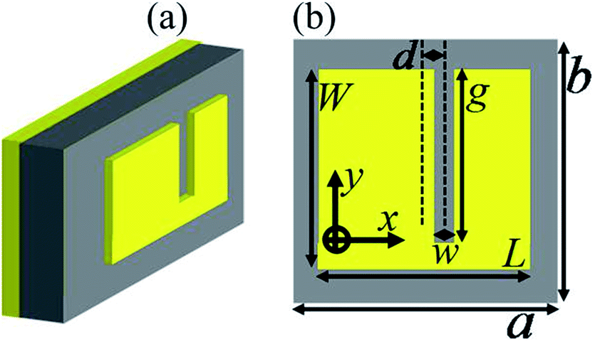 | ||
| Fig. 1 Three-dimensional structure drawing (a) and front view (b) of the suggested broadband PMA. | ||
Results and discussion
Fig. 2(a) shows the resonance absorption spectra of the suggested broadband PMA as a function of frequency. As presented, two resonance features can be obtained. Firstly, the single-sized resonator exhibits four near perfect absorption frequency points marked as B1, B2, B3, and B4. The basic principles of these frequency points are due to four different loading positions of the single-sized resonator. The following paragraphs will provide detailed theoretical evidence. Secondly, a wide frequency range of resonance bandwidths is gained because of the four close frequency points. Greater than 50% incident light energy can be absorbed in a continuous spectral range of 1.24 THz to 2.85 THz to form a large bandwidth of 1.62 THz having a central frequency of 2.05 THz. The RRB of the suggested broadband PMA can be up to 79.02%, which is higher than that of the broadband PMAs obtained utilizing methods A and B. The large resonance bandwidth (or RRB) with the simple single-sized structure design should be able to find a wide range of applications in related areas of optoelectronic technology. The suggested resonator should be highly sensitive to polarization angles of the incident light because of the asymmetric structural dimensions in two orthogonal directions. As observed in Fig. 2(b), the broadband performance can be changed to dual-band absorption when the E field of the light is parallel to the y-axis (i.e., 90° polarization).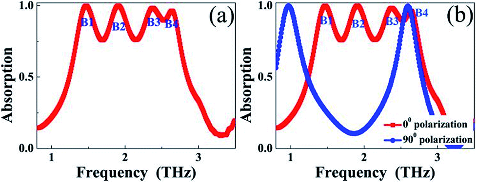 | ||
| Fig. 2 (a) Resonance absorption spectra of the broadband PMA as a function of frequency; (b) resonance absorption spectra of the broadband PMA as a function of frequency at two different polarization angles. | ||
In fact, the presence of the elongated slot in the rectangular-shaped plate plays a crucial role in the formation of the broadband absorption. To gain an intuitive understanding, we compare the resonance absorption spectra of the rectangular-shaped plate with or without the elongated slot. Because we only examine the influence of the elongated slot, the other parameters of these two kinds of PMAs must be the same. As revealed in Fig. 3(a) for the case without the elongated slot (i.e., the plate resonator), two separated frequency points with near 100% absorption located at 1.04 THz and 2.65 THz are realized, which is clearly different from the resonance performance of the plate resonator having the elongated slot (i.e., the designed structure in Fig. 1), see Fig. 3(b), indicating that the existence of the elongated slot in the rectangular-shaped plate indeed plays a great role in obtaining the broadband absorption.
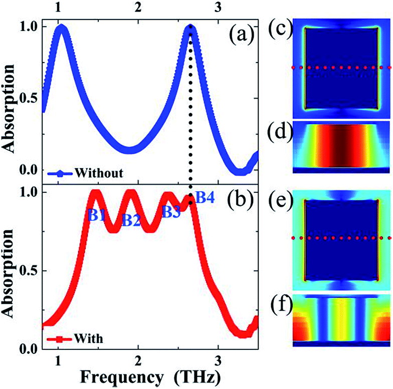 | ||
| Fig. 3 Resonance absorption response of the Au resonator without (a) or with (b) the elongated slot; the electric (|E|, in the resonator central plane) fields of the first (c) and second (e) frequency points of Fig. 3(a); the magnetic (|Hy|, perpendicular to the resonator along the red dotted line) fields of the first (d) and second (f) frequency points of Fig. 3(a). | ||
Interestingly, we found that the second frequency point of the plate resonator in Fig. 3(a) is very close to the last frequency point (mode B4) of the broadband PMA in Fig. 3(b), see the black dotted line in Fig. 3(a) and (b), which suggests that they should have a similar physical origin. The electric (|E|) and magnetic (|Hy|) fields of the two discrete frequency points are plotted in Fig. 3(c)–(f) to explore the physical mechanism of the dual-band absorption of the plate resonator. As shown, the |E| field of the first frequency point in Fig. 3(c) is highly focused on both edges of the entire plate resonator, which is similar to that of the |E| distribution of the second frequency point in Fig. 3(e). However, the |Hy| field distributions of the two frequency points in the insulator dielectric sheet are clearly different. Only one |Hy| field assembling region in Fig. 3(d) is observed for the first frequency point, whereas three |Hy| field assembling regions can be obtained for the second frequency point, see Fig. 3(f). These results indicate that the first and the second frequency points of the dual-band absorption in Fig. 3(a) can be respectively ascribed to first-order and third-order responses of the plate resonator.30–32
To better explore the basic mechanism of the broadband PMA in Fig. 2(a) and 3(b), the distributions of the electric (|E|) and magnetic (|Hy|) fields of the four different but close frequency points (i.e., B1, B2, B3, and B4) are plotted in Fig. 4. We clearly observed that each frequency point exhibits different field distribution features. That is to say, the loading positions of these modes in the broadband PMA are different. For example, for the frequency point B1, its |E| fields in Fig. 4(a) are intensely gathered at both edges of the left and right sides of the suggested resonator. Meanwhile two |Hy| field assembling regions are obtained in the insulator dielectric sheet of the broadband PMA, see Fig. 4(e). It should be noted that the frequency point B1 is not the second-order response of the suggested resonator, but should be the combined effect of two first-order resonance modes of the resonator because the two assembling regions are actually caused by the magnetic resonances of the left and right sides of the suggested resonator.
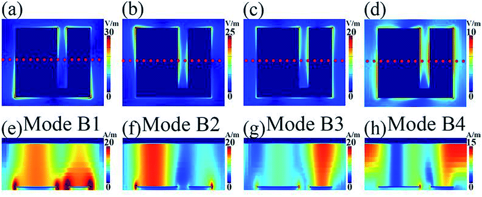 | ||
| Fig. 4 The electric (|E|, in the resonator central plane) fields of the frequency points B1 (a), B2 (b), B3 (c), and B4 (d); the magnetic (|Hy|, perpendicular to the resonator along the red dotted line) fields of the frequency points B1 (e), B2 (f), B3 (g), and B4 (h). | ||
For the frequency point B2, we noticed that the |E| field in Fig. 4(b) and the |Hy| field in Fig. 4(f) are mostly concentrated on both edges of the left side of the resonator and the left side of the insulator dielectric sheet, respectively, indicating that the mode B2 is the first-order response of the left side of the suggested resonator. Because the |E| field of the frequency point B3 in Fig. 4(c) and the corresponding |Hy| field of Fig. 4(f) are strongly focused on both edges of the right side of the resonator and the right side of the insulator dielectric sheet, respectively, the mode B3 can be attributed to the first-order response of the right side of the suggested resonator. Furthermore, the frequency point B4 should be due to the third-order response of the entire resonator because its corresponding |Hy| field in Fig. 4(h) has three assembling regions (and its |E| field in Fig. 4(d) is chiefly confined at both edges of the left and right sides of the resonator (i.e., the entire resonator)).30–32 Although the presence of the elongated slot in the rectangular-shaped plate can suppress the initial first-order response of the plate resonator (of course its third-order response mode is retained), three new resonance modes can be introduced. Consequently, the superposed effect of the three newly generated modes (B1, B2, and B3) and the slight frequency shift of the third-order response (B4) lead to the broadband absorption. The simple single-sized resonator with a large absorption bandwidth (or RRB) can show many advantages over previous broadband PMAs obtained using methods A and B.
Based on the above analyses, one can draw the conclusion that the presence of the elongated slot in the rectangular-shaped plate presents the ability to yield the frequency points B1, B2, and B3. Therefore, the size changes of the elongated slot in the rectangular-shaped plate will inevitably affect the resonance performance, in particular the first three frequency points of the broadband PMA. For example, the lengths of the left side and right side of the resonator are both decreased with the increase of the slot length w because the entire resonator length L is fixed. The length decreases of the left side and right side of the resonator can lead to the frequency increases of the frequency points B1, B2, and B3 because of the inversely proportional relationship between the length and the resonance frequency.
As shown in Fig. 5(a), we clearly observed that the frequencies of the first three frequency points gradually increase with the increase of the slot length w, whereas the frequency shift of the B4 is neglected. The deviation value (d) of the elongated slot in the rectangular-shaped plate also influences the broadband absorption performance of the suggested resonator. As given in Fig. 5(b), the frequencies of the frequency points B1, B2 and B3 are highly controlled by the deviation value (d) because its change can simultaneously tune the sizes of the left side and right side of the resonator. Different from the slot parameter change of the length w and deviation d, the variation of the slot width g in Fig. 5(c) has only a slight effect on the frequency points of B1, B3, and B4 because the change in g does not affect the sizes of the left side and right side of the resonator. Certainly, if one can vary the entire length L of the resonator and keep the sizes of the elongated slot unchanged, the frequencies of the four frequency points (B1, B2, B3, and B4) should be significantly affected by the length L, as revealed in Fig. 5(d).
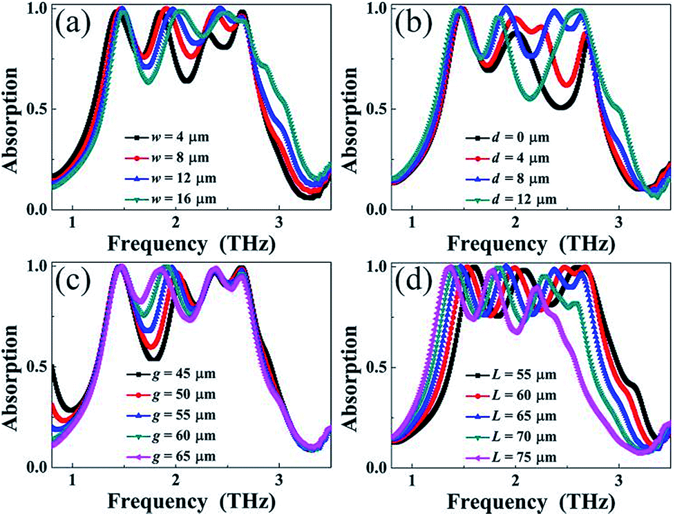 | ||
| Fig. 5 Resonance absorption spectra of the suggested broadband PMA as a function of frequency with changes in different parameters such as the (a) slot length w, (b) slot deviation value d, (c) slot width g, and (d) entire resonator length L. | ||
Conclusions
In conclusion, a novel and simple PMA structure design based on a rectangular-shaped Au plate having an elongated slot placed on an insulator dielectric sheet (with a thickness of 14um) and an Au plane is utilized to realize broadband absorption performance at terahertz frequencies. The suggested device possesses four discrete but close frequency points, and the combination of these frequency points yields a broadband absorption. A continuous spectral range of 1.62 THz with a central frequency of 2.05 THz with absorption higher than 50% can be gained. The RRB of the broadband PMA is 79.02%, which is superior to that of previous broadband PMAs using methods A and B. Both of the basic principles of the broadband absorption and the dependence of the absorption responses on the parameter changes of the resonance structure are further discussed. In contrast to previous investigations that mainly employed methods A and B, here the design concept with the simple single-sized unit structure could be used as an alternative to realize broadband integrated terahertz absorption devices.Conflicts of interest
There are no conflicts to declare.Acknowledgements
This research was funded by the National Natural Science Foundation of China grant number 11647143, the Natural Science Foundation of Jiangsu grant number BK20160189, the China Postdoctoral Science Foundation grant number 2019M651692, the Jiangsu Postdoctoral Science Foundation grant number 2018K113C, and the Fundamental Research Funds for the Central Universities grant number JUSRP51721B.References
- N. I. Landy, S. Sajuyigbe, J. J. Mock, D. R. Smith and W. J. Padilla, Phys. Rev. Lett., 2008, 100, 207402 CrossRef CAS PubMed.
- I. Faniayeu and V. Mizeikis, Appl. Phys. Express, 2017, 10, 062001 CrossRef.
- B. X. Wang, C. Tang, Q. Niu, Y. He and T. Chen, Nanoscale Res. Lett., 2019, 14, 64 CrossRef PubMed.
- T. D. Dao, K. Chen, S. Ishii, A. Ohi, T. Nabatame, M. Kitajima and T. Nagao, ACS Photonics, 2015, 2, 964–970 CrossRef CAS.
- K. Liu, S. Jiang, D. Ji, X. Zeng, N. Zhang, Y. Xu and Q. Gan, IEEE Photonics Technol. Lett., 2015, 27, 1539–1542 CAS.
- X. Zhao, Y. Wang, J. Schalch, G. Duan, K. Cremin, J. Zhang, C. Chen, R. D. Averitt and X. Zhang, ACS Photonics, 2019, 6, 830–837 CrossRef CAS.
- J. Y. Suen, K. Fan and W. J. Padilla, Adv. Opt. Mater., 2019, 7, 1801632 CrossRef CAS.
- W. Wang, X. Yang, T. S. Luk and J. Gao, Appl. Phys. Lett., 2019, 114, 021103 CrossRef.
- A. Ghobadi, H. Hajian, B. Butun and E. Ozbay, ACS Photonics, 2018, 5, 4203–4221 CrossRef CAS.
- G. Duan, J. Schalch, X. Zhao, J. Zhang, R. D. Averitt and X. Zhang, Phys. Rev. B, 2018, 97, 035128 CrossRef CAS.
- S. Liu, H. Chen and T. J. Cui, Appl. Phys. Lett., 2015, 106, 151601 CrossRef.
- P. Liu and T. Lan, Appl. Opt., 2017, 56, 4201–4205 CrossRef CAS PubMed.
- X. He, S. Yan, Q. Ma, Q. Zhang, P. Jia, F. Wu and J. Jiang, Opt. Commun., 2015, 340, 44–49 CrossRef CAS.
- W. Pan, X. Yu, J. Zhang and W. Zeng, IEEE Photonics Technol. Lett., 2016, 28, 2335–2338 Search PubMed.
- J. Fan, D. Xiao, Q. Wang, Q. Liu and Z. Ouyang, Appl. Opt., 2017, 56, 4388–4391 CrossRef CAS PubMed.
- Y. J. Kim, Y. J. Yoo, K. W. Kim, J. Y. Rhee, Y. H. Kim and Y. P. Lee, Opt. Express, 2015, 23, 3861–3868 CrossRef CAS PubMed.
- J. Zhu, Z. Ma, W. Sun, F. Ding, Q. He, L. Zhou and Y. Ma, Appl. Phys. Lett., 2014, 105, 021102 CrossRef.
- N. Zhang, P. Zhou, S. Wang, X. Weng, J. Xie and L. Deng, Opt. Commun., 2015, 338, 388–392 CrossRef CAS.
- D. Xiao, K. Tao and Q. Wang, Plasmonics, 2016, 111, 389–394 CrossRef.
- Y. Wang, M. Song, M. Pu, Y. Gu, C. Hu, Z. Zhao, C. Wang, H. Yu and X. Luo, Plasmonics, 2016, 11, 1201–1206 CrossRef CAS.
- W. Guo, Y. Liu and T. Han, Opt. Express, 2016, 24, 20586–20592 CrossRef CAS.
- C. Gong, M. Zhan, J. Yang, Z. Wang, H. Liu, Y. Zhao and W. Liu, Sci. Rep., 2016, 6, 32466 CrossRef CAS PubMed.
- A. K. Azad, W. J. M. Kort-Kamp, M. Sykora, N. R. Weisse-Bernstein, T. S. Luk, A. J. Taylor, D. A. R. Dalvit and H. T. Chen, Sci. Rep., 2016, 6, 20347 CrossRef CAS PubMed.
- X. Ming and Q. Tian, Plasmonics, 2017, 12, 117–124 CrossRef.
- B. X. Wang, IEEE J. Sel. Top. Quantum Electron., 2017, 23, 4700107 Search PubMed.
- K. Ustun and G. T. Sayan, J. Opt. Soc. Am. B, 2017, 34, D86–D94 CrossRef.
- Y. Liu, S. Gu, C. Luo and X. Zhao, Appl. Phys. A, 2012, 108, 19–24 CrossRef CAS.
- W. Ma, Y. Wen and X. Yu, Opt. Express, 2013, 21, 30724–30730 CrossRef PubMed.
- R. Feng, J. Qiu, L. Liu, W. Ding and L. Chen, Opt. Express, 2014, 22, A1713–A1724 CrossRef PubMed.
- G. Dayal and S. A. Ramakrishna, J. Opt., 2014, 16, 094016 CrossRef.
- G. Dayal and S. A. Ramakrishna, J. Phys. D Appl. Phys., 2015, 48, 035105 CrossRef.
- A. Sellier, T. V. Teperik and A. Lustrace, Opt. Express, 2013, 21, A997–A1006 CrossRef PubMed.
| This journal is © The Royal Society of Chemistry 2019 |