
A generic green solvent concept boosting the power conversion efficiency of all-polymer solar cells to 11%†
Zhenye
Li
a,
Lei
Ying
 *a,
Peng
Zhu
a,
Wenkai
Zhong
a,
Ning
Li
*b,
Feng
Liu
c,
Fei
Huang
*a and
Yong
Cao
a
*a,
Peng
Zhu
a,
Wenkai
Zhong
a,
Ning
Li
*b,
Feng
Liu
c,
Fei
Huang
*a and
Yong
Cao
a
aInstitute of Polymer Optoelectronic Materials and Devices, State Key Laboratory of Luminescent Materials and Devices, South China University of Technology, Guangzhou, 510640, P. R. China. E-mail: msleiying@scut.edu.cn; msfhuang@scut.edu.cn
bInstitute of Materials for Electronics and Energy Technology (i-MEET), FAU Erlangen-Nürnberg, 91058 Erlangen, Germany. E-mail: ning.li@fau.de
cDepartment of Physics and Astronomy, Shanghai Jiao Tong University, Shanghai 200240, P. R. China
First published on 20th November 2018
Abstract
Advances in organic photovoltaic technologies have always been closely associated with a deeper understanding of bulk-heterojunction (BHJ) microstructure morphology, which is generally governed by the ink-formulation based on a single solvent or solvent mixtures. The relatively slow progress in all-polymer solar cells (all-PSCs) is mainly due to the significant difficulty in mastering their intricate BHJ morphology dealing with entanglements of polymer chains, limiting their performance typically to 8–10%. In this work, we demonstrate that the performance of all-PSCs can be further developed to a benchmark value of 11% by manipulating the BHJ morphology using a green solvent system based on cyclopentyl methyl ether (CPME). The generic applicability of the superior ink-formulation is successfully validated in four different all-polymer solar cells, exhibiting great promise of advancing all-PSCs towards industrial production and commercialization.
Broader contextPolymer solar cells (PSCs) are a type of thin film solar cell consisting of polymeric semiconducting materials, which can directly convert solar energy to urgently needed electrical energy and can be manufactured through continuous roll-to-roll processing. Among so far developed PSCs, the cases consisting of a polymeric donor and polymeric acceptor – all polymer solar cells (all-PSCs) – in the active layer are of particular interest on account of their properties of light-weight, flexibility, and long-term stability. Despite the fact that the power conversion efficiencies of all-PSCs have been significantly improved from about 3% to 10% by rational molecular design and advanced device engineering, the overall photovoltaic performance still lags behind that of devices based on small molecule non-fullerene acceptors. To continuously boost the photovoltaic performance of all-PSCs, here we compare the material–processing–property relationships based on three green ether solvents with different boiling points, and provide important guidelines for choosing a green solvent to achieve the full potential of all-PSCs by tuning the microstructure morphology as well as the molecular orientation. |
As a promising clean energy technology, polymer solar cells that comprise p-type conjugated polymers as the electron donor and n-type organic semiconductors as the electron acceptor have attracted considerable interest,1–6 primarily due to their specific advantages of light weight, great potential for portable electronic devices, and short energy payback time.7–12 Recently emerged non-fullerene acceptors (NFAs) significantly promoted the progress of high-performance PSCs by virtue of obviously enhanced solar photon harvesting capability.13–19 In particular, all-polymer solar cells (all-PSCs) that utilise conjugated polymers as both the electron-donor and electron-acceptor in the photoactive layer have attracted much attention, because of their outstanding photochemical, thermal, and mechanical stabilities.20–22 The power conversion efficiencies (PCEs) of all-PSCs have been significantly improved from about 3% to over 10% through rational molecular design and sophisticated processing of bulk-heterojunction (BHJ) films.23–28
From the perspective of practical applications of all-PSCs, however, further improving photovoltaic performance while keeping excellent processablility by using green solvents is of critical importance. One solution to address these issues is to develop novel n-type and p-type polymers, which have complementary absorption to enhance solar photon utilisation, and have appropriate energy levels that can ensure effective exciton separation and charge carrier transportation. However, the payoff of such a process remains uncertain owing to the lack of rational molecular design principles to achieve a delicate balance of each single photovoltaic parameter. An alternative solution is to control the aggregation behaviour of polymer chains and morphology of BHJ films by using an ideal solvent system that can dissolve both the polymer donor and acceptor at certain concentrations, and allow for fabricating high-quality films, wetting the surface of substrates, and promoting formation of desired phase separation and molecular orientation.29,30
As the processing solvent provides a significant opportunity to adjust the drying kinetics and allows for fine-tuning of the BHJ microstructures, it is of high priority to choose suitable solvents with appropriate boiling points (b.p.) and volatility.31 In this respect, we carefully go through the solvent database with this selection criterion and choose a non-chlorinated hydrophobic ether solvent, cyclopentyl methyl ether (CPME), which has a unique composition that imparts excellent stability under acidic and basic conditions and resists formation of peroxides. Regarding the previously used green solvent of 2-methyltetrahydrofuran32 (2-MeTHF, b.p. of 78 °C) and the commonly used tetrahydrofuran (THF, b.p. of 66 °C), the higher boiling point (106 °C) of CPME offers extended drying time that can facilitate the formation of ordered structures during the film drying procedure.33 More importantly, CPME can replace hazardous halogenated solvents to dissolve a wide range of conjugated polymers to achieve sustainability and reduce environmental and operational costs.34
In this work, we demonstrated the use of CPME as a generic solvent to process a range of photoactive layers of all-PSCs with impressively high photovoltaic performance. By optimizing the processing conditions of a BHJ film consisting of a wide-bandgap electron-donating polymer containing imide-functionalised benzotriazole units (PTzBI-Si, Fig. 1a) and the electron-accepting poly{[N,N-9-bis(2-octyldodecyl)naphthalene-1,4,5,8-bis(dicarboximide)-2,6-diyl]-alt-5,5′-(2,2′-bithiophene)} (N2200, Fig. 1a),35 the resulting all-PSC presented an unprecedented PCE of 11.0%, which obviously outperforms that processed with green-solvent 2-MeTHF. The absorption spectrum of the pristine PTzBI-Si film displayed a well-defined absorption band centred at approximately 580 nm, which is complementary to that of the pristine N2200 film with two distinct absorption bands centred at about 380 nm (corresponding to the π–π* transition) and 700 nm (Fig. 1b). The absorption profile of PTzBI-Si:N2200 in CPME shows bathochromic shifts with respect to its absorption profiles in 2-MeTHF and THF (Fig. 1c), implying stronger aggregates in the CPME solution, as evidenced by the fact that the CPME solution was much darker in colour (Fig. 1d) than the 2-MeTHF and THF solutions. The PTzBI-Si:N2200 blend film processed with CPME exhibited a slightly enhanced absorption coefficient than that processed with 2-MeTHF in the range of 300–480 nm, both of which exhibited a slightly higher absorption coefficient in the range of 300–750 nm than that processed with THF (Fig. 1e). It is worth noting that at a high temperature of 120 °C, PTzBI-Si, N2200, and PTzBI-Si![[thin space (1/6-em)]](https://www.rsc.org/images/entities/char_2009.gif) :N2200 (1:0.5, wt/wt) can be easily dissolved in CPME at a high concentration of 20, 10, and 15 mg mL−1, respectively (see Table S1 in the ESI†). Despite the N2200 solution becomes more viscous than the PTzBI-Si solution after being cooled down to room temperature of about 25 °C, no gel state solids precipitated from the PTzBI-Si:N2200 (1:0.5, wt/wt) solution, and the solution still can be used for the fabrication of thin films by the spin-coating technique.
:N2200 (1:0.5, wt/wt) can be easily dissolved in CPME at a high concentration of 20, 10, and 15 mg mL−1, respectively (see Table S1 in the ESI†). Despite the N2200 solution becomes more viscous than the PTzBI-Si solution after being cooled down to room temperature of about 25 °C, no gel state solids precipitated from the PTzBI-Si:N2200 (1:0.5, wt/wt) solution, and the solution still can be used for the fabrication of thin films by the spin-coating technique.
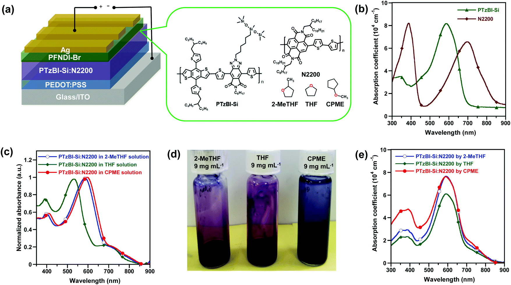 | ||
| Fig. 1 (a) Molecular structures of PTzBI-Si, N2200, 2-MeTHF, THF and CPME; (b) UV-vis-NIR absorption spectra of pristine films of PTzBI-Si and N2200; (c) normalised UV-vis-NIR absorption spectra of PTzBI-Si:N2200 (1:0.5, wt/wt) solution in 2-MeTHF, THF and CPME; (d) photographs of PTzBI-Si:N2200 (1:0.5, wt/wt) in 2-MeTHF, THF and CPME with the same concentration of 9 mg mL−1; and (e) normalised UV-vis-NIR absorption spectra of PTzBI-Si:N2200 (1:0.5, wt/wt) blend films processed with 2-MeTHF, THF and CPME. | ||
The photovoltaic performance of all-PSCs processed with 2-MeTHF, THF and CPME was evaluated in a conventional device structure: ITO/PEDOT:PSS/PTzBI-Si:N2200/PFNDI-Br/Ag. A water/alcohol soluble poly[(9,9-bis(3′-((N,N-dimethyl)-N-ethylammonium)propyl)-2,7-fluorene)-alt-5,5′-bis(2,2′-thiophene)-2,6-naphthalene-1,4,5,8-tetracaboxylic-N,N′-di(2-ethylhexyl)imide]dibromide (PFNDI-Br) layer (5 nm) was deposited onto the photoactive layer to facilitate charge extraction.36 We compared several solvents and found that 2-MeTHF, THF and CPME were superior to traditional halogenated solvents, such as chlorobenzene (CB), dichlorobenzene (DCB) and chloroform (CF). Because 2-MeTHF, THF and CPME are green solvents, our initial optimization of devices was devoted to screening non-halogenated solvent additives,37 and we found that dibenzyl ether (DBE) is effective and can lead to enhanced photovoltaic performance (Table S2, ESI†). The donor-to-acceptor ratio in the active layer was fixed at a weight ratio of 2:1 and the thermal annealing temperature was optimized at 110 °C for 10 min (Table S3, ESI†). The J–V characteristics of 2-MeTHF, THF and CPME-processed all-PSCs under AM 1.5G simulated solar light at 100 mW cm−2 and external quantum efficiency (EQE) spectra are illustrated in Fig. 2a and b, and the corresponding device parameters are summarised in Table 1.
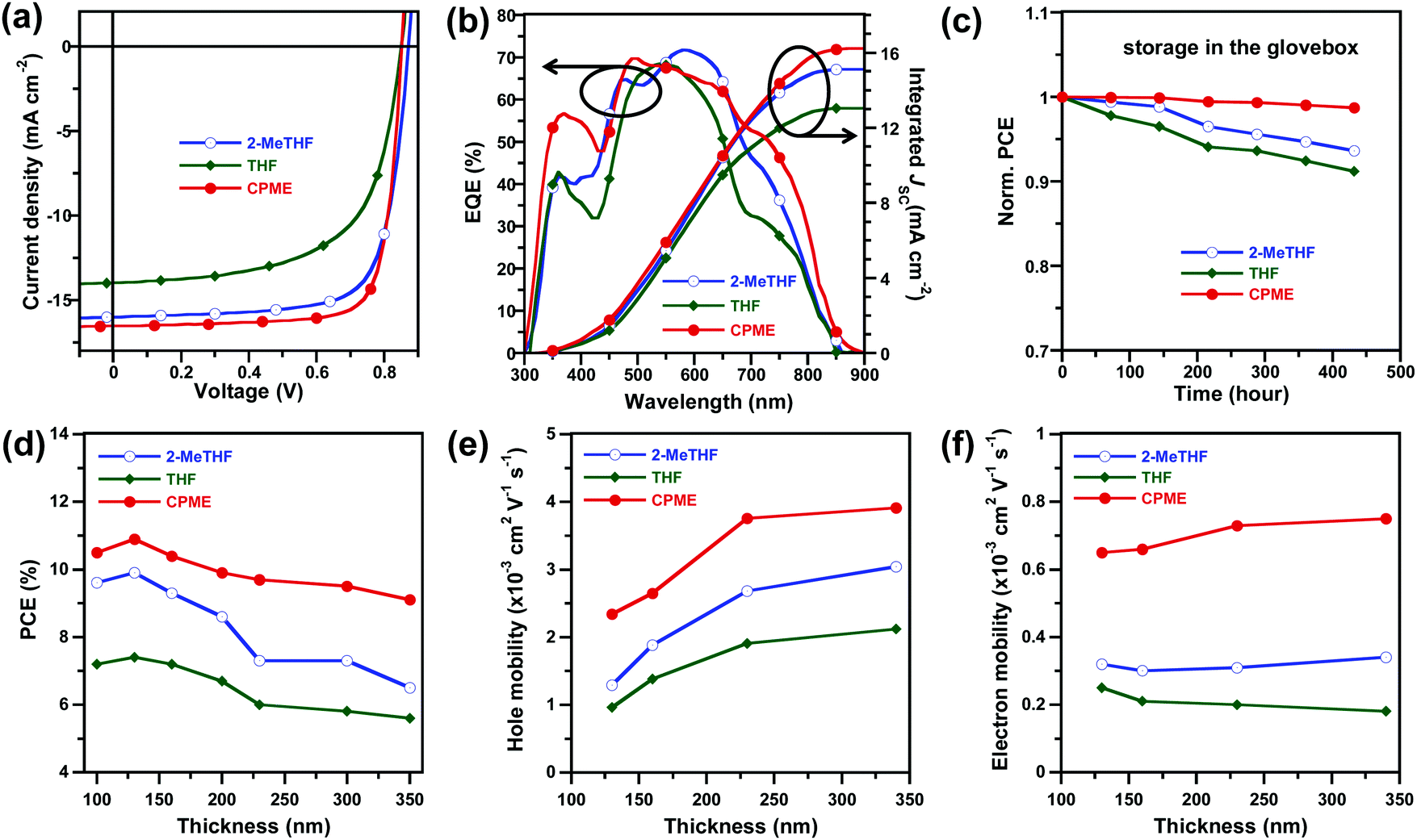 | ||
| Fig. 2 (a) J–V characteristics, (b) EQE spectra and (c) normalized PCE during storage in the glovebox for different times of 2-MeTHF, THF and CPME processed all-PSCs composed of PTzBI-Si:N2200 (1:0.5, wt/wt). (d–f) PCE, hole and electron mobility versus thickness characteristics for 2-MeTHF, THF and CPME processed all-PSCs. | ||
| Solventa | Thickness (nm) | V OC (V) | J SC (mA cm−2) | J SC,EQE (mA cm−2) | FF (%) | PCEavgd (%) | PCEmax (%) |
|---|---|---|---|---|---|---|---|
|
a PTzBI-Si:N2200 = 2:1 (wt/wt) treated at 110 °C for 10 min.
b Obtained from J–V measurements.
c Obtained from the integration of EQE spectra.
d The PCE values are obtained from 12 separate devices.
e With 0.5 vol% DBE.
|
|||||||
| 2-MeTHFe | 130 | 0.85 ± 0.01 | 15.6 ± 0.2 | 15.2 ± 0.3 | 73.1 ± 0.5 | 9.9 ± 0.2 | 10.1 |
| 350 | 0.85 ± 0.01 | 17.0 ± 0.3 | 16.7 ± 0.1 | 44.7 ± 0.8 | 6.4 ± 0.2 | 6.6 | |
| THFe | 130 | 0.85 ± 0.01 | 13.6 ± 0.4 | 13.1 ± 0.4 | 63.4 ± 0.5 | 7.4 ± 0.2 | 7.6 |
| 350 | 0.85 ± 0.01 | 12.1 ± 0.4 | 11.7 ± 0.3 | 54.1 ± 0.5 | 5.5 ± 0.1 | 5.6 | |
| CPMEe | 130 | 0.85 ± 0.01 | 16.5 ± 0.3 | 16.2 ± 0.4 | 77.9 ± 0.9 | 10.8 ± 0.2 | 11.0 |
| 350 | 0.85 ± 0.01 | 18.6 ± 0.4 | 18.2 ± 0.2 | 58.0 ± 0.6 | 9.0 ± 0.3 | 9.3 | |
The device processed with 2-MeTHF exhibited an impressively high PCE of 10.1%, with an open-circuit voltage (VOC) of 0.86 V, short-circuit current density (JSC) of 15.6 ± 0.2 mA cm−2, and a fill factor (FF) of 73.1 ± 0.5%. The devices processed with THF exhibited a decreased PCE of 7.6% due to the decreased JSC (13.6 ± 0.4 mA cm−2) and FF (63.4 ± 0.5%). In contrast, an obviously improved PCE of 11.0% was obtained using CPME as the processing solvent because of its improved JSC (16.5 ± 0.3 mA cm−2) and FF (77.9 ± 0.9%). To our knowledge, the PCE of 11% represents the highest value reported so far for single junction all-PSCs.36,38 Of particular interest is that the CPME-processed devices exhibited excellent storage lifetime stability, for which the PCE retained over 98% of its original value after 400 h storage in the glovebox (Fig. 2c). It is also worth noting that the PCE retained over 99% of its original value (Fig. S1a, ESI†) after 48 h annealing at the moderate temperature of 80 °C in the glovebox and retained over 93% of its original value (Fig. S1b, ESI†) after 48 h illumination under 1 sun irradiation in the glovebox, demonstrating the good thermal and photo-stability of the all-PSCs. The accuracy of the observed JSC values was confirmed by integrating the EQE spectra with the AM 1.5G solar spectrum (Fig. 2b) with a discrepancy less than 5%. The device processed with CPME exhibited a slightly higher response than that processed with 2-MeTHF in the range of 300–480 nm while the device processed with THF exhibited a significantly lower EQE response across almost the entire spectral region than that processed with 2-MeTHF.
The remarkably high FF values of CPME processed all-PSCs enabled us to fabricate efficient devices with a thick photoactive layer. Thick-film all-PSCs were fabricated with the same conventional device structure, and the thickness of the photoactive layer ranged from 100 to 350 nm. The J–V characteristics and EQE spectra of all-PSCs processed with 2-MeTHF, THF and CPME with a range of film thicknesses are summarised in Tables S4–S6 and Fig. S2–S4 (ESI†). For 2-MeTHF and THF processed all-PSCs, the PCE decreased quickly with increased film thickness, and the PCE only remained at 6.6% and 5.6% (Table 1) with a thickness of 350 nm, respectively. Notably, for CPME processed all-PSCs, the PCE remained at 9.3% (Table 1) with a thickness of 350 nm, which demonstrates the great potential of using CPME as the solvent toward high-throughput roll-to-roll mass production.
To explore the reasons for the high performance of the all-PSC processed with CPME in thick-film, we investigated the charge carrier mobility of neat PTzBI-Si, neat N2200, and PTzBI-Si:N2200 blends processed with 2-MeTHF, THF and CPME with different thicknesses by the space-charge-limited current (SCLC) method (see Fig. S5, S6 and Tables S7, S8, ESI†). The hole mobility (μh) and electron mobility (μe) as a function of film thickness characteristics for the all-PSCs processed with different solvents are plotted in Fig. 2e and f, respectively. For PTzBI-Si:N2200 blend films processed with 2-MeTHF, THF and CPME, one can note that μh increased with the thickness while μe almost did not vary depending on the film thickness, which was consistent with the similar trend observed in neat PTzBI-Si and neat N2200, respectively (see Fig. S5 and Table S7, ESI†). Furthermore, devices processed with CPME presented higher μh and μe values than those of devices processed with 2-MeTHF and THF at film thicknesses of 130–340 nm, which was beneficial to reduce the accumulation of space charges, thus leading to notably high PCEs of 11.0% at 130 nm and 9.3% at 340 nm. Further investigation indicated that the CPME-processed devices exhibited the highest charge generation and extraction, and the lowest charge recombination rates (Fig. S7 and Tables S9–S11, ESI†).
Grazing-incidence wide-angle X-ray scattering (GIWAXS) measurements were conducted to investigate the order structures of PTzBI-Si:N2200 films. Both PTzBI-Si and N2200 in pure films assume a face-on orientation with respect to the substrate, as indicated by the strong (010) π–π stacking peaks in the out-of-plane (OOP) direction and the (100) lamellar stacking peaks in the in-plane (IP) direction (Fig. S8a and b, ESI†). PTzBI-Si shows a (010) peak in the OOP direction at 1.73 Å−1 and a (100) peak in the in-plane (IP) direction at 0.25 Å−1. For the N2200 neat film, a (010) peak in the OOP direction arises at 1.60 Å−1, while a (100) peak in the IP direction is observed at 0.26 Å−1; a (001) peak is located at 0.47 Å−1 in the IP direction, originating from the rigid and flat in-chain repeat unit correlation. Here the crystal coherence length (CCL) was calculated according to the Scherrer equation CCL = 2π/Δq, where Δq is the full width at half-maximum (FWHM) of a diffraction peak.39
The two-dimensional GIWAXS textures of blend films show combined features of each component (Fig. 3a), with relevant parameters summarized in Table 2. The PTzBI-Si:N2200 film processed with 2-MeTHF shows a broad (010) peak in the OOP direction at 1.71 Å−1 (d = 3.68 Å) with a CCL of 2.01 nm and a (100) peak in the IP direction at 0.26 Å−1 with a CCL of 13.36 nm. In contrast, the blend film processed with THF shows decreased molecular co-facial packing, as indicated by the (010) peak in the OOP direction at 1.70 Å−1 (d = 3.69 Å) with a decreased CCL of 1.89 nm, suggesting the weaker packing of the polymers in the THF processed blend. We suppose that the decreased molecular co-facial packing is associated with the reduced pre-aggregation of PTzBI-Si in THF solution, since the film exhibited a much lower absorption coefficient in the range of 500–700 nm (corresponding to PTzBI-Si) than that obtained from the film processed with 2-MeTHF. The PTzBI-Si:N2200 film processed with CPME exhibits enhanced molecular co-facial packing, as indicated by the sharper (010) peak in the OOP direction at 1.72 Å−1 (d = 3.65 Å) with an increased CCL of 2.22 nm and the sharper (100) peak in the IP direction at 0.25 Å−1 with an increased CCL of 18.47 nm, indicating the π–π stacking and crystal size of polymers were further improved, in good agreement with the boosted charge carrier mobility and the overall photovoltaic performance. The enhanced molecular co-facial packing may be correlated to N2200 aggregation in 2-MeTHF and CPME solutions, as the CPME processed film exhibited a slightly higher absorption coefficient in the range of 300–450 nm (corresponding to N2200) than that processed with 2-MeTHF.
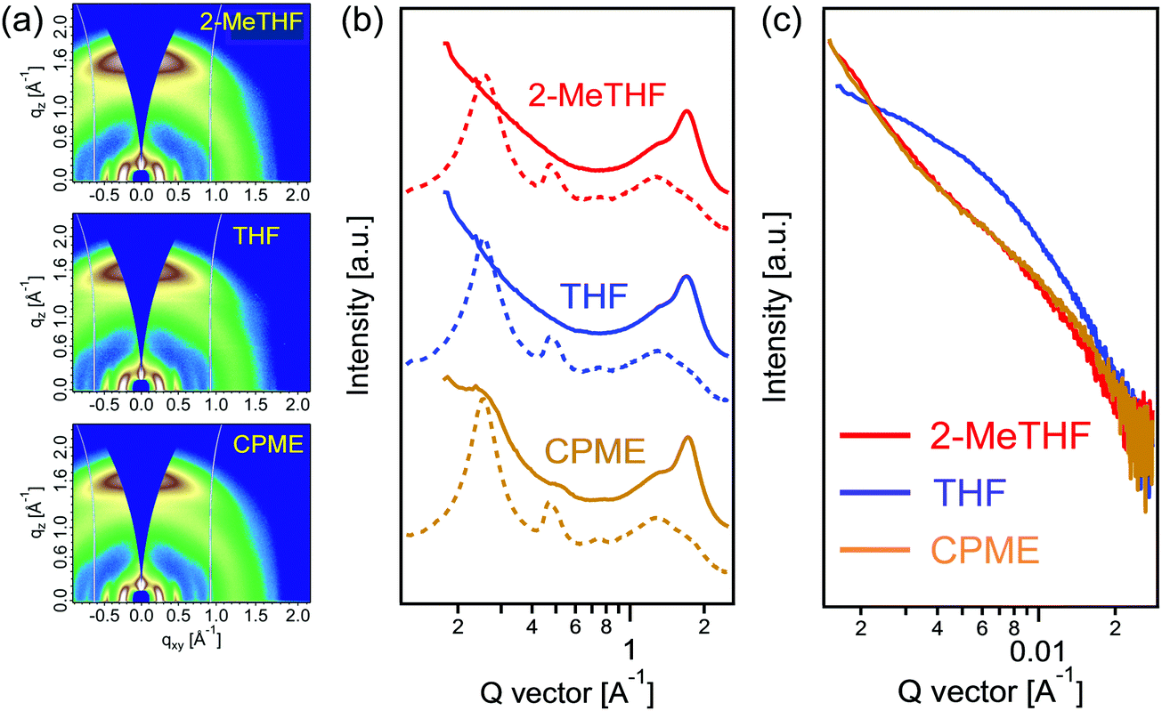 | ||
| Fig. 3 GIWAXS patterns of PTzBI-Si:N2200 film processed with 2-MeTHF, THF and CPME (a); one-dimensional integrated scattering profiles for the corresponding films (b); and RSoXS profiles for the corresponding films (c). | ||
| Solvent | Peak | Peak location (Å−1) | π–π stacking distance (Å) | FWHM (Å−1) | Crystal coherence length (nm) |
|---|---|---|---|---|---|
| 2-MeTHF | (100) in IP | 0.26 | — | 0.047 | 13.36 |
| (010) in OOP | 1.71 | 3.68 | 0.313 | 2.01 | |
| THF | (100) in IP | 0.26 | — | 0.043 | 14.60 |
| (010) in OOP | 1.70 | 3.69 | 0.333 | 1.89 | |
| CPME | (100) in IP | 0.25 | — | 0.034 | 18.47 |
| (010) in OOP | 1.72 | 3.65 | 0.283 | 2.22 |
The length scale of phase separation of PTzBI-Si:N2200 films processed with 2-MeTHF, THF and CPME was investigated using resonant soft X-ray scattering (RSoXS), with the results shown in Fig. 3c. The RSoXS circular average profiles were extracted at an optimum photon energy of 285.4 eV, which is sensitive to the polymer 1s–π*C![[double bond, length as m-dash]](https://www.rsc.org/images/entities/char_e001.gif) C bond transition. The PTzBI-Si:N2200 film processed with THF showed a discernable broad hump at ∼0.0062 Å−1, corresponding to a domain-to-domain distance of ∼101 nm. When the blend film was processed by 2-MeTHF or CPME, the RSoXS intensity was less defined, for which the total scattering intensity (TSI) decreased significantly (see the fitting result of the I(q)q2 ∼ q profiles in Fig. S9, ESI†), indicative of the drastically improved polymer mixing between PTzBI-Si and N2200.40 The scattering peak shifted to a q value of ∼0.0070 Å−1 (∼88 nm) for the 2-MeTHF processed blend, and further moved to 0.0096 Å−1 (∼65 nm) for the CPME processed blend. Such small phase separation with highly improved polymer mixing is quite advantageous for the exciton splitting and charge transport, leading to a large enhancement of JSC and FF in the 2-MeTHF and CPME based solar cell devices.
C bond transition. The PTzBI-Si:N2200 film processed with THF showed a discernable broad hump at ∼0.0062 Å−1, corresponding to a domain-to-domain distance of ∼101 nm. When the blend film was processed by 2-MeTHF or CPME, the RSoXS intensity was less defined, for which the total scattering intensity (TSI) decreased significantly (see the fitting result of the I(q)q2 ∼ q profiles in Fig. S9, ESI†), indicative of the drastically improved polymer mixing between PTzBI-Si and N2200.40 The scattering peak shifted to a q value of ∼0.0070 Å−1 (∼88 nm) for the 2-MeTHF processed blend, and further moved to 0.0096 Å−1 (∼65 nm) for the CPME processed blend. Such small phase separation with highly improved polymer mixing is quite advantageous for the exciton splitting and charge transport, leading to a large enhancement of JSC and FF in the 2-MeTHF and CPME based solar cell devices.
To prove the universality of the CPME solvent concept, all-PSCs consisting of PTB7-Th:N2200, J51:N2200 and PTzBI:N2200 (Fig. 4a) were fabricated and characterized. These polymer donors were chosen because they were commonly used in the literatures for all-PSCs with relatively high efficiency. The J–V characteristics of these three different all-PSCs processed with 2-MeTHF, THF and CPME and EQE spectra are illustrated in Fig. 4b–g, and the corresponding device parameters are summarised in Table S12 (in the ESI†). As expected, the universality of the CPME solvent concept was found to result in highly efficient all-PSCs based on these three different all-PSC systems. The PTB7-Th:N2200, J51:N2200 and PTzBI:N2200 devices processed with CPME achieved superior PCEs of 6.9%, 8.7% and 9.9%, respectively, compared to the control devices processed with 2-MeTHF or THF. These very promising findings demonstrated the great potential of using CPME as a generic green solvent to master the optimum BHJ morphology of all-PSCs towards high performance, promising stability and industrial viability.
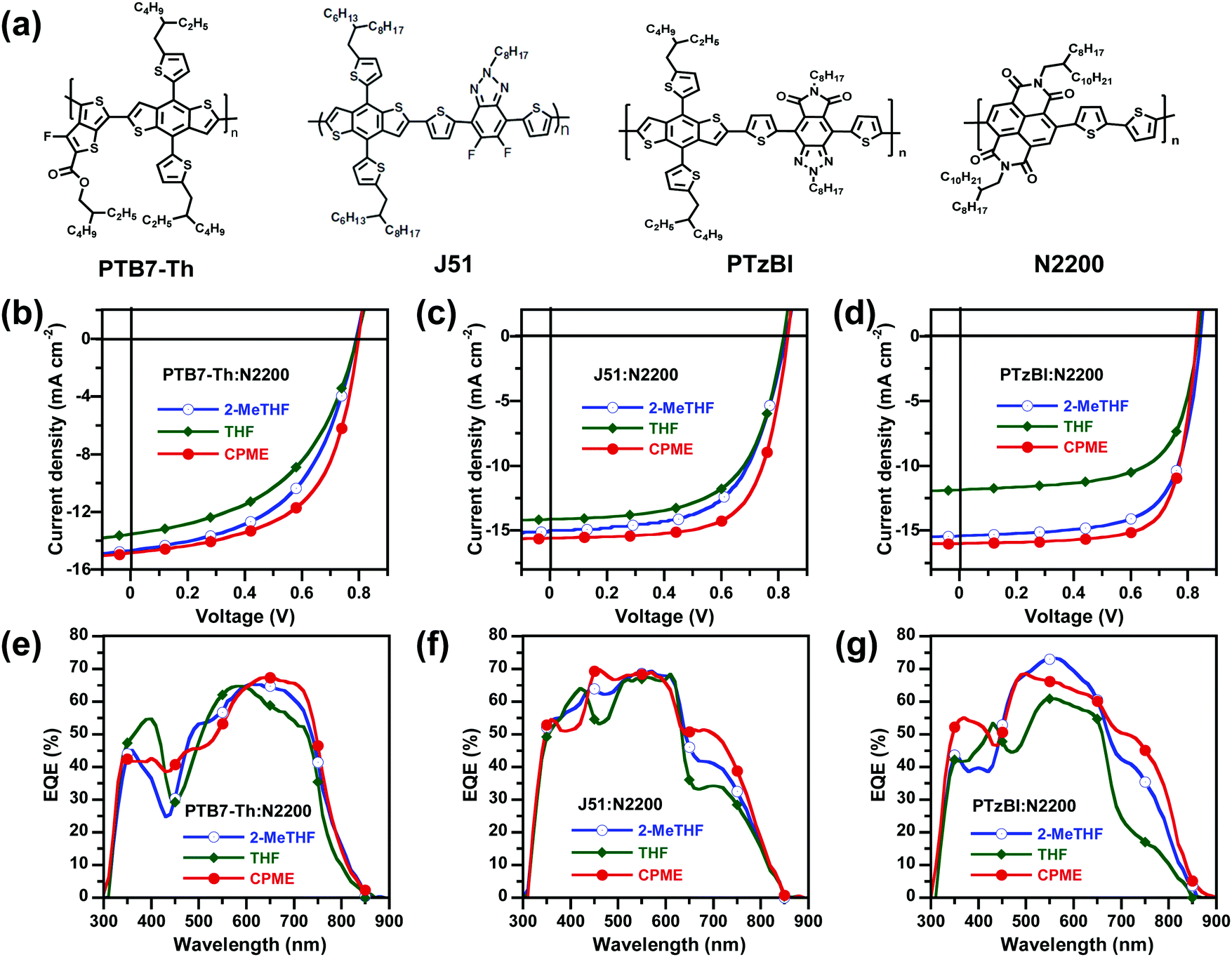 | ||
| Fig. 4 Generality of 2-MeTHF, THF and CPME for all-PSCs. (a) Chemical structure of donors and acceptors for the generality test of 2-MeTHF, THF and CPME. (b–d) J–V characteristics and (e–g) EQE spectra of PTB7-Th:N2200, J51:N2200 and PTzBI:N2200-based all-PSCs processed with 2-MeTHF, THF and CPME. | ||
In summary, we developed an advanced green solvent concept based on CPME to further improve and stabilize the performance of all-PSCs comprising the wide-bandgap conjugated PTzBI-Si and the n-type copolymer N2200. The CPME processed all-PSCs exhibited an unprecedented PCE of 11% with improved stability, which is clearly superior to that of 2-MeTHF processed all-PSCs. The unprecedented PCE is attributable to the enhanced absorption profile, efficient energy transfer, enhanced charge mobility, and improved morphology. Of particular importance is that the all-PSCs processed with CPME exhibit a remarkable PCE of 9.3% with a thickness of the active layer of 350 nm, indicating the great promise of this green solvent to be used for high-throughput roll-to-roll mass production. Moreover, these morphology–property–performance correlations established in our model system provide important guidelines for choosing the optimal green solvent to tune the molecular orientation in realizing the full potential of all-PSCs. Furthermore, the CPME solvent is readily available and applicable to various all-PSC systems, and may also be used as a generic solvent for processing other high performance organic electronics, such as organic field effect transistors, organic light-emitting diodes and organic photodetectors.
Conflicts of interest
There are no conflicts to declare.Acknowledgements
This work was financially supported by the National Natural Science Foundation of China (No. 21520102006, 21822505, 91633301 and 51521002). Portions of this research used the resources of beamline 7.3.3 and 11.0.1.2 at the Advanced Light Source, Materials Science Division, The Molecular Foundry, Lawrence Berkeley National Laboratory, which was supported by the Office of Science, Office of Basic Energy Sciences, of the U.S. Department of Energy under Contract No. DE-AC02-05CH11231.Notes and references
- J. Zhao, Y. Li, G. Yang, K. Jiang, H. Lin, H. Ade, W. Ma and H. Yan, Nat. Energy, 2016, 1, 15027 CrossRef CAS.
- M. Li, K. Gao, X. Wan, Q. Zhang, B. Kan, R. Xia, F. Liu, X. Yang, H. Feng, W. Ni, Y. Wang, J. Peng, H. Zhang, Z. Liang, H.-L. Yip, X. Peng, Y. Cao and Y. Chen, Nat. Photonics, 2016, 11, 85 CrossRef.
- T. Kumari, M. L. Sang, S. H. Kang, S. Chen and C. Yang, Energy Environ. Sci., 2017, 10, 258 RSC.
- H. Bin, L. Gao, Z. G. Zhang, Y. Yang, Y. Zhang, C. Zhang, S. Chen, L. Xue, C. Yang, M. Xiao and Y. Li, Nat. Commun., 2016, 7, 13651 CrossRef CAS PubMed.
- B. M. Savoie, S. Dunaisky, T. J. Marks and M. A. Ratner, Adv. Energy Mater., 2015, 5, 1400891 CrossRef.
- Y. Jin, Z. Chen, M. Xiao, J. Peng, B. Fan, L. Ying, G. Zhang, X.-F. Jiang, Q. Yin, Z. Liang, F. Huang and Y. Cao, Adv. Energy Mater., 2017, 6, 1700944 CrossRef.
- J. Zhao, Y. Li, G. Yang, K. Jiang, H. Lin, H. Ade, W. Ma and H. Yan, Nat. Energy, 2016, 1, 15027 CrossRef CAS.
- M. Li, K. Gao, X. Wan, Q. Zhang, B. Kan, R. Xia, F. Liu, X. Yang, H. Feng, W. Ni, Y. Wang, J. Peng, H. Zhang, Z. Liang, H.-L. Yip, X. Peng, Y. Cao and Y. Chen, Nat. Photonics, 2016, 11, 85 CrossRef.
- T. Kumari, M. L. Sang, S. H. Kang, S. Chen and C. Yang, Energy Environ. Sci., 2017, 10, 258 RSC.
- H. Bin, L. Gao, Z. G. Zhang, Y. Yang, Y. Zhang, C. Zhang, S. Chen, L. Xue, C. Yang, M. Xiao and Y. Li, Nat. Commun., 2016, 7, 13651 CrossRef CAS PubMed.
- S. B. Darling and F. You, RSC Adv., 2013, 3, 17633 RSC.
- Y. Jin, Z. Chen, M. Xiao, J. Peng, B. Fan, L. Ying, G. Zhang, X.-F. Jiang, Q. Yin, Z. Liang, F. Huang and Y. Cao, Adv. Energy Mater., 2017, 6, 1700944 CrossRef.
- W. Zhao, S. Li, H. Yao, S. Zhang, Z. Yun, Y. Bei and J. Hou, J. Am. Chem. Soc., 2017, 139, 7148 CrossRef CAS PubMed.
- J. Zhu, Z. Ke, Q. Zhang, J. Wang, S. Dai, Y. Wu, Y. Xu, Y. Lin, W. Ma, W. You and X. Zhan, Adv. Mater., 2017, 29, 1704713 Search PubMed.
- S. J. Xu, Z. Zhou, W. Liu, Z. Zhang, F. Liu, H. Yan and X. Zhu, Adv. Mater., 2017, 29, 1704510 CrossRef PubMed.
- Y. Yang, Z. G. Zhang, H. Bin, S. Chen, L. Gao, L. Xue, C. Yang and Y. Li, J. Am. Chem. Soc., 2016, 138, 15011 CrossRef CAS PubMed.
- B. Fan, K. Zhang, X. F. Jiang, L. Ying, F. Huang and Y. Cao, Adv. Mater., 2017, 27, 1606396 CrossRef PubMed.
- S. Chen, Y. An, G. K. Dutta, Y. Kim, Z.-G. Zhang, Y. Li and C. Yang, Adv. Funct. Mater., 2017, 27, 1603564 CrossRef.
- D. Deng, Y. Zhang, J. Zhang, Z. Wang, L. Zhu, J. Fang, B. Xia, Z. Wang, K. Lu, W. Ma and Z. Wei, Nat. Commun., 2016, 7, 13740 CrossRef CAS PubMed.
- A. Facchetti, Mater. Today, 2013, 16, 123 CrossRef CAS.
- H. Kang, W. Lee, J. Oh, T. Kim, C. Lee and B. J. Kim, Acc. Chem. Res., 2016, 49, 2424 CrossRef CAS PubMed.
- X. Gu, H. Yan, T. Kurosawa, B. C. Schroeder, K. L. Gu, Y. Zhou, J. W. F. To, S. D. Oosterhout, V. Savikhin, F. Molina-Lopez, C. J. Tassone, S. C. B. Mannsfeld, C. Wang, M. F. Toney and Z. Bao, Adv. Energy Mater., 2016, 6, 1601225 CrossRef.
- L. Gao, Z. G. Zhang, L. Xue, J. Min, J. Zhang, Z. Wei and Y. Li, Adv. Mater., 2016, 28, 1884 CrossRef CAS PubMed.
- Z. Zhang, Y. Yang, J. Yao, L. Xue, S. Chen, X. Li, W. Morrison, C. Yang and Y. Li, Angew. Chem., Int. Ed., 2017, 129, 1 CrossRef.
- S. Liu, Z. Kan, S. Thomas, F. Cruciani, J. L. Brédas and P. M. Beaujuge, Angew. Chem., Int. Ed., 2016, 55, 1 CrossRef.
- C. Dou, X. Long, Z. Ding, Z. Xie, J. Liu and L. Wang, Angew. Chem., Int. Ed., 2016, 55, 1436 CrossRef CAS PubMed.
- Y. Guo, Y. Li, O. Awartani, H. Han, J. Zhao, H. Ade, Y. He and D. Zhao, Adv. Mater., 2017, 29, 1700309 CrossRef PubMed.
- Z. Li, B. Fan, B. He, L. Ying, W. Zhong, F. Liu, F. Huang and Y. Cao, Sci. China: Chem., 2018, 61, 427 Search PubMed.
- C. Mu, P. Liu, W. Ma, K. Jiang, J. Zhao, K. Zhang, Z. Chen, Z. Wei, Y. Yi, J. Wang, S. Yang, F. Huang, A. Facchetti, H. Ade and H. Yan, Adv. Mater., 2014, 26, 7224 CrossRef CAS PubMed.
- C. McDowell and G. C. Bazan, Curr. Opin. Green Sustainable Chem., 2017, 5, 49 CrossRef.
- C. R. McNeill, Energy Environ. Sci., 2012, 5, 5653 RSC.
- (a) Y. Zhou, K. L. Gu, X. Gu, T. Kurosawa, H. Yan, Y. Guo, G. I. Koleilat, D. Zhao, M. F. Toney and Z. Bao, Chem. Mater., 2016, 28, 5037 CrossRef CAS; (b) C.-D. Park, T. A. Fleetham, J. Li and B. D. Vogt, Org. Electron., 2011, 12, 1465 CrossRef CAS.
- C. McDowell, M. Abdelsamie, M. F. Toney and G. C. Bazan, Adv. Mater., 2018, 30, 1707114 CrossRef PubMed.
- I. Burgués-Ceballos, F. Machui, J. Min, T. Ameri, M. M. Voigt, Y. N. Luponosov, S. A. Ponomarenko, P. D. Lacharmoise, M. Campoy-Quiles and C. J. Brabec, Adv. Funct. Mater., 2014, 24, 1449 CrossRef.
- B. Fan, L. Ying, P. Zhu, F. Pan, F. Liu, J. Chen, F. Huang and Y. Cao, Adv. Mater., 2017, 29, 1703906 CrossRef PubMed.
- Z. Wu, C. Sun, S. Dong, X.-F. Jiang, S. Wu, H. Wu, H.-L. Yip, F. Huang and Y. Cao, J. Am. Chem. Soc., 2016, 138, 2004 CrossRef CAS PubMed.
- (a) N. Liang, K. Sun, Z. Zheng, H. Yao, G. Gao, X. Meng, Z. Wang, W. Ma and J. Hou, Adv. Energy Mater., 2016, 6, 1600060 CrossRef; (b) J. Yin, W. Zhou, L. Zhang, Y. Xie, Z. Yu, J. Shao, W. Ma, J. Zeng and Y. Chen, Macromol. Rapid Commun., 2017, 38, 1700428 CrossRef PubMed.
- Z. Li, R. Xie, W. Zhong, B. Fan, J. Ali, L. Ying, F. Liu, N. Li, F. Huang and Y. Cao, Sol. RRL, 2018, 1800196 CrossRef.
- D.-M. Smilgies, J. Appl. Crystallogr., 2009, 42, 1030 CrossRef CAS PubMed.
- B. A. Collins, Z. Li, J. R. Tumbleston, E. Gann, C. R. McNeill and H. Ade, Adv. Energy Mater., 2013, 3, 65 CrossRef CAS.
Footnote |
| † Electronic supplementary information (ESI) available. See DOI: 10.1039/c8ee02863j |
| This journal is © The Royal Society of Chemistry 2019 |