
 Open Access Article
 This Open Access Article is licensed under a Creative Commons Attribution-Non Commercial 3.0 Unported Licence
Ultrathin Fe-NiO nanosheets as catalytic charge reservoirs for a planar Mo-doped BiVO4 photoanode†
Lei
Li
ab,
Xiaogang
Yang
 *abc,
Yan
Lei
ac,
Haili
Yu
ad,
Zhongzheng
Yang
ab,
Zhi
Zheng
*ac and
Dunwei
Wang
e
*abc,
Yan
Lei
ac,
Haili
Yu
ad,
Zhongzheng
Yang
ab,
Zhi
Zheng
*ac and
Dunwei
Wang
e
aKey Laboratory for Micro-Nano Energy Storage and Conversion Materials of Henan Province, College of Advanced Materials and Energy, Institute of Surface Micro and Nanomaterials, Xuchang University, Xuchang, Henan 461000, China. E-mail: xiaogang.yang@gmail.com; zzheng@xcu.edu.cn
bHenan Key Material Laboratory, North China University of Water Resources and Electric Power, Zhengzhou, Henan 450045, China
cHenan Joint International Research Laboratory of Nanomaterials for Energy and Catalysis, Xuchang University, Xuchang, Henan 461000, China
dCollege of Chemistry and Molecular Engineering, Zhengzhou University, Zhengzhou, Henan 450001, China
eDepartment of Chemistry, Merkert Chemistry Center, Boston College, 2609 Beacon St., Chestnut Hill, MA 02467, USA
First published on 19th September 2018
Abstract
The energy conversion efficiency of a photoelectrochemical system is intimately connected to a number of processes, including light absorption, charge excitation, separation and transfer processes. Of these processes, the charge transfer rate at the electrode|electrolyte interface is the slowest and, hence, the rate-limiting step causing charge accumulation. Such an understanding underpins efforts focused on applying highly active electrocatalysts, which may contribute to the overall performance by augmenting surface charge accumulation, prolonging charge lifetime or facilitating charge transfer. How the overall effect depends on these individual possible mechanisms has been difficult to study previously. Aiming at advancing knowledge about this important interface, we applied first-order serial reactions to elucidate the charge excitation, separation and recombination kinetics on the semiconductor|electrocatalyst interfaces in air. The study platform for the present work was prepared using a two-step Mo-doped BiVO4 film modified with an ultrathin Fe-doped NiO nanosheet, which was derived from an Fe-doped α-Ni(OH)2 nanosheet by a convenient precipitation and ion-exchange method. The simulation results of the transient surface photovoltage (TSPV) data showed that the surface charge accumulation was significantly enhanced, even at an extremely low coverage (0.12–120 ppm) using ultra-thin Fe-NiO nanosheets. Interestingly, no improvement in the charge separation rate constants or reduction of recombination rate constants was observed under our experimental conditions. Instead, the ultra-thin Fe-NiO nanosheets served as a charge storage layer to facilitate the catalytic process for enhanced performance.
Introduction
The photoelectrochemical (PEC) reaction is one of the most promising methods for solar energy conversion and storage and, therefore, has attracted tremendous research attention.1,2 The key components include a semiconducting photo-absorber, and a co-catalyst to accelerate the surface redox reactions in the electrolyte.3 Due to the complicated requirements of the high efficient light absorption/excitation, separation and transfer kinetics, the heterogeneous materials possess great advantages over single-component ones.4–6 For example, the co-catalyst on the semiconductors can display various effects on the charge reaction rates.7–9 Given the extremely sluggish surface redox reaction rate (ms–s) and the short charge lifetime (ps–μs),10 how to manipulate the heteronanostructure or the interface between the semiconductor and the catalyst becomes critical for the high-efficiency charge separation/transfer rate.6,11Take BiVO4 (Eg = 2.4 eV) as an example. It is an earth abundant n-type semiconductor that has been widely applied as a photoanode for water splitting12–14 or CO2 reduction.15,16 Generally, it suffers from slow charge separation/transport, slow electron mobility,17 and poor water oxidation kinetics.18 Various strategies have been proposed to address these issues,19 such as (1) increasing the doping density by introducing Mo or W dopants,20,21 or oxygen vacancies by hydrogen treatments;22 (2) incorporating an SnO2 underlayer to reduce interface charge recombination;23 (3) fabricating heterojunctions for larger built-in electric fields;24,25 (4) enlarging surface band bending by long time photocharging26,27 or electrochemical treatments;28 and (5) employing oxygen evolution catalysts (OECs) to lower the activation energy (Ea) and increase the charge transfer rate. For BiVO4/OEC heteronanostructures, crystalline NiOOH/FeOOH, Ni(OH)2, NiO, CoO, Co3O4, amorphous Co-Pi and NiFeOx have been successfully used, showing significant PEC performance enhancements. At least four possible functions of the OECs have been proposed. First, a typical catalyst can increase the charge separation/transfer, resulting in the decrease of surface recombination.13,29 For example, by coating BiVO4 with a FeOOH layer, researchers obtained a substantially increased hole collection at the solid|liquid junction, which is responsible for the high measured photocurrents.18,30 For another example, an ultrathin CoOx (1 nm) catalyst layer allowed greater hole collection as opposed to faster kinetics.31 By comparison, amorphous cobalt phosphate (Co-Pi: 30 nm) increased the charge transfer kinetics.32 Second, the suppression of surface recombination led to a high photovoltage (band bending), causing faster surface reactions with higher photocurrent.33 To this end, the Durrant group employed transient absorption spectroscopy (TAS) to demonstrate the retardation of electron/hole recombination.34 They did not observe any evidence of catalytic behaviours. When studying the CoPi, FeOOH or NiFeOx catalysts on BiVO4 with the intensity modulated photocurrent spectroscopy (IMPS),35 the photocurrent was found to be limited by fast surface recombination rate rather than surface catalysis. Third, charge separation/transfer can be intrinsically increased by the built-in electronic field in heterojunctions (e.g., p–n junction).36,37 Chang et al. introduced discrete p-type Co3O4 co-catalysts on BiVO4 to form a p–n heterojunction, which was shown to facilitate charge separation, increasing surface reactions and suppressing recombination at the interface.38 Similarly, a Ni-doped CoOx uniform layer (p-type) increased the surface band bending with a cathodic Von shift and photocurrent increase.39 This surface band bending enhancement also resulted in the reduction of surface charge recombination on the NiO/CoOx/BiVO4 photoanode.37 In addition, the hole-storage layer effect of ferrihydrite was suggested on BiVO4 and Ta3N5 photoanodes.40,41 Despite these advances, it has been difficult to fully understand what the true causes are for the observed performance improvements at the semiconductor|electrocatalyst interface. Therefore, charge behaviours at the semiconductor|electrocatalyst interface remain relatively poorly understood, presenting a challenge for further improvement of PEC systems. This interface is thus of great importance and has attracted significant research attention.
To discern the thermodynamic and kinetic influences at this interface, the Boettcher group has successfully employed a dual-working-electrode (DWE) method to scrutinize the photovoltage and charge transfer differences between the adaptive and dense semiconductor|catalyst junctions in the electrolyte.42,43 Their secondary working electrodes could be used to either probe or control the catalyst/electrolyte interface in situ, so that the electrochemical potential/current of the catalyst can be independently measured.9 Separately, the Durrant group has measured a 3rd order oxygen evolution reaction (OER) order with regard to surface hole concentrations on BiVO4 under higher surface hole densities (>1 nm−2) based on photoinduced absorption analysis (PIA).44 A 1st order OER rate dependence on the hole concentration was found when the surface hole density was low (<1 nm−2). Results like these raise important questions concerning the detailed processes and their influence on the overall performance of photoelectrodes in PEC reactions. For instance, at low surface coverage, does a co-catalyst influence the system by changing the kinetics or surface energetics? How does the charge accumulated at the semiconductor|electrocatalyst interface contribute to the photoelectrochemical reactions? Similar questions were difficult to answer using existing methodologies. To correct this deficiency, here we report a simple transient surface photovoltage (TSPV) analysis45–47 that can directly monitor the accumulated charges at the semiconductor|air or semiconductor|electrocatalyst interface, especially under the open-circuit condition. We show that the technique is an important tool to advance our understanding of the interface charge phenomena. The merit of this TSPV method is the ability to individually study charge separation/transfer at the semiconductor|electrocatalyst interface with negligible redox reactions because the system is an open circuit.
For this body of research, we chose crystalline ultrathin Fe-doped NiOx (Fe-NiO) nanosheets as an oxygen evolution catalyst on planar Mo-doped BiVO4 (Mo-BiVO4) films. The system was first studied in air before in a contacting electrolyte, as our goal was to elucidate the charge separation kinetics. Different from the previously reported synthesis method of Ni(OH)2 catalyst by plasma deposition48 or in situ electrochemical decomposition,13,14,30 we simply prepared ultrathin Fe-doped Ni(OH)2 nanosheets through a precipitation and ion-exchange method. The catalyst was spin-coated onto the Mo-BiVO4 films and thermally converted to a discrete ultrathin Fe-NiO catalyst layer. Next, we applied the TSPV to investigate the surface charge accumulation kinetics on the semiconductor|electrocatalyst interface in air. Simulation of the kinetics was carried out, and we observed an apparent first-order dependence of charge separation and recombination on charge concentrations. An increased surface charge accumulation was observed at the Mo-BiVO4/Fe-NiO interface, implying that the catalyst serves as a charge “reservoir”, despite its relatively low loading. The Fe-NiO modified Mo-BiVO4 photoanode showed a significant overall enhancement for water oxidation in an alkaline electrolyte (1 M NaOH) with high charge transfer efficiencies. The charge separation and transfer efficiencies at the semiconductor|electrolyte interface were also investigated during the PEC test with and without Fe-doped NiO catalyst, respectively.
Experimental sections
Materials
FTO substrate was purchased from Huanan Xiangcheng Sci. Co. (Shenzhen); the Bi target was obtained from Zhongcheng New Materials Co. (Beijing). The chemical reagents such as vanadyl acetylacetonate (VO(acac)2), molybdenyl acetylacetonate (MoO2(acac)2), NaOH, Ni(NO3)2·6H2O, Fe(NO3)3·9H2O, and dimethyl sulfoxide (DMSO) are commercially available from Sinopharm Chemical reagent (Shanghai), Sigma-Aldrich and Alfa Aesar Chem.Preparation of Mo-doped BiVO4 film
FTO glass was ultrasonically cleaned in a H2O/H2O2/NH3·H2O (1/1/1 v/v/v) solution, washed with deionized (DI) water and naturally dried in air. Next, a Bi metal film (40 nm) was vacuum deposited on a FTO substrate with a K575XD Ar ion sputter. Following the previously reported methods,13 Mo-doped BiVO4 films were prepared by a two-step process. Briefly, 30 μL of VO(acac)2 in DMSO (0.5 M) was cast coated on the Bi film (1 cm × 2 cm) and dried in an oven, before being slowly heated in a muffle furnace to 450 °C (heating rate at 2 °C per minute) and maintained at 450 °C for 4 h. The resulting brownish films were soaked in 1 M NaOH solution for 20–30 min, rinsed with DI water to remove excess vanadate impurities, followed by post annealing at 500 °C for 2 h. The obtained films were denoted as undoped BiVO4. In the second step, a mixed solution containing MoO2(acac)2 and VO(acac)2 in a DMSO solution (Mo/V = 5% in molar ratio) was cast on the BiVO4 films, slowly heated to 450 °C and sequentially treated at 500 °C for 2 h. After the impurities were removed using NaOH and DI water, the obtained film was denoted as two-step Mo-doped BiVO4 (2-Mo-BiVO4). Single conversion process was used for homogenous 1-Mo-BiVO4 with the same mixed Mo/V precursor solution.Synthesis of ultrathin Fe-doped NiO nanosheets on 2-Mo-BiVO4
25 mL of Ni(NO3)2 solution (0.1 M) was added into 1 M NaOH solution (6 mL) dropwise under vigorous stirring for 10 min. The resulting light greenish Ni(OH)2 precipitate was centrifugated and washed using DI water several times, which was re-dispersed in 20 mL DI water. 300 μL of Fe(NO3)3 (1 M) was added to the above Ni(OH)2 dispersion, allowing ion exchange under ultrasonic treatment for 2 h. The resulting brownish dispersion was centrifugated/washed in DI water several times to remove the excess ions. In the end, the obtained precipitation was denoted as Fe-doped Ni(OH)2. It was re-dispersed in DI water (120 μg mL−1 or 120 ppm), which was spin-coated onto 2-Mo-BiVO4 films. Typically, 50 μL of the Fe-doped Ni(OH)2 dispersion was spread on a 2-Mo-BiVO4 film spinning at 3000 rpm for 60 s. After thermal annealing at 300 °C for 2 h in air, the 2-Mo-BiVO4/Fe-NiO-120 film was obtained. For the other loading amounts, the dispersion for spin-coating was diluted to 12 ppm, 1.2 ppm and 0.12 ppm, respectively.Structure, optical and photoelectronic characterization
X-ray powder diffraction (XRD) was conducted on a Bruker X-ray diffractometer (D8 Advance, Cu Kα, λ = 1.5418 Å) in the range of 10°–70°. Scanning electron microscopy (SEM) was observed on a field emission scanning electron microscope (FEI, Nova NanoSEM450). High resolution TEM image and electron diffraction were obtained on a transmission electron microscope (FEI Tecnai G2 F20) under 200 kV. The thickness/height image, photoconductive topology and Kelvin probe force microscopy were collected on a conductive atomic force microscope (C-AFM, Bruker Dimension Icon, coupled with AM 1.5G light) under ambient conditions, using conductive AFM probes (Bruker, PFTUNA and SCM-PIT, respectively). The Fe-doped NiO samples (>80 cm2) were dissolved into dilute HNO3; after that, the surface catalyst loading amount was checked by inductive coupled plasma mass spectroscopy (ICP-MS, Agilent 7700). The XPS data were collected on a spectrometer (Thermo Scientific Escalab 250Xi), and Raman spectra were collected on a Renishaw confocal Raman microscope (in Via Reflex) using a green laser (532 nm) in the range of 200–1000 cm−1. The optical properties of the produced films were measured in the transmission mode with a UV-vis spectrophotometer (Agilent Tech. Cary 5000). The transient surface photovoltage was investigated on a home-made capacitor-like spectroscope,46,49 where a Quantel Nd:YAG nanosecond laser (Brilliant Eazy, BRILEZ/IR) was used as the excitation source (355 nm, 4 ns, spot area of 0.24 cm2), coupled with a digital oscilloscope (Tektronix, TDS 3054C, 500 MHz) and pre-amplifier for recording. A sandwich structure of FTO|mica|BiVO4 (on FTO) was assembled in a metal faradaic container, where a mica (∼70 μm) was used as spacer.Photoelectrochemical and impedance measurements
The photoelectrode was prepared by connecting a Cu wire with silver adhesive to a FTO substrate, encapsulated with insulated cross-linked rubber only with the active area exposed. The PEC measurements were carried out using a three-electrode configuration on a potentiostat (CHI 660E, Shanghai), with a counter electrode (Pt wire) and a reference electrode (Hg/HgO, in 1 M NaOH, 0.098 V vs. NHE) in an electrolyte solution (1 M NaOH, pH = 13.5). The potential was converted to the reversible hydrogen electrode (RHE) scale following this equation: E = EHg/HgO + 0.098 + 0.059 × 13.5. A standard simulated solar illuminator (AM 1.5G on Newport 94023, 100 mW cm−2) was chosen as the light source. The polarization J–V curves were recorded using a linear sweep technique with a scanning rate of 20 mV s−1 in the range of 0.2–1.6 V (vs. RHE) with backside illumination. The Mott–Schottky plots of the Mo-BiVO4 films were collected in the dark in 1 M NaOH (containing 2 mM Fe(CN)63−/Fe(CN)64−) to determine the flat band position. The electrochemical impedance spectroscopy (EIS) of the electrodes was measured at 1.5 V vs. RHE from 105 to 0.1 Hz with an AC amplitude of 5 mV in a 1 M NaOH electrolyte. The cyclic voltammetry (CV) curves were analysed in the same electrolyte from 1.1 to 1.6 V vs. RHE.Results and discussion
To investigate the charge separation at the Mo-BiVO4/Fe-NiO interface, we start to prepare the Fe-doped NiO catalyst and Mo-BiVO4 semiconductor separately before integrating them together. For the synthesis of the Fe-NiO catalyst, Ni(OH)2 was freshly precipitated from a solution, which was converted to Fe-doped nickel hydroxide under ultrasonic agitation. In Fig. 1(a), this layered structure can be well confirmed by the XRD pattern (α-Ni(OH)2·0.75H2O, JCPDS card, no. 38-0715) in the bottom (black curve), where only (003) and (006) diffraction peaks were shown. Then, the ultrathin Fe-doped NiO nanosheet was obtained through a thermal conversion of the layered hydroxides at 300 °C. In Fig. 1(a), the red curve displays three peaks at 37.05°, 43.31° and 62.83°, corresponding to a slightly contracted lattice constant of a = 4.185 Å of a face-centred cubic NiO structure (JCPDS card, no. 65-2901) and close to the NiO nanosheets (a = 4.182 Å, with ∼0.1% lattice strain) prepared by similar processes (XRD pattern in Fig. S1†). This lattice increment of NiO after Fe doping agreed well with a previous report.50 In Fig. 1(b), the binding energies of Fe2p and Ni2p electrons are shown, respectively. The Fe2p peak can be deconvoluted as Fe2p3/2, Fe2p1/2 and a pre-2p3/2 peak at 711.7 eV, 723.5 eV and 704.4 eV, respectively. This is in good agreement with a Fe3+ state.50 For the Ni2p peaks, two sets of Ni2p3/2, Ni2p1/2 and their satellite peaks were shown at 855.6 eV, 873.2 eV and 861.3 eV and 879.2 eV, respectively, corresponding to a Ni2+ in the Fe-doped NiO product.50 XPS showed that the element molar ratio of Fe/Ni was ca. 27%/73%. The higher Fe doping level may be due to the comparable radius of Fe3+ (64.5 pm) and Ni2+ (69 pm) with a six-fold coordination,51 and/or large surface/volume ratio to release the lattice stress (strain).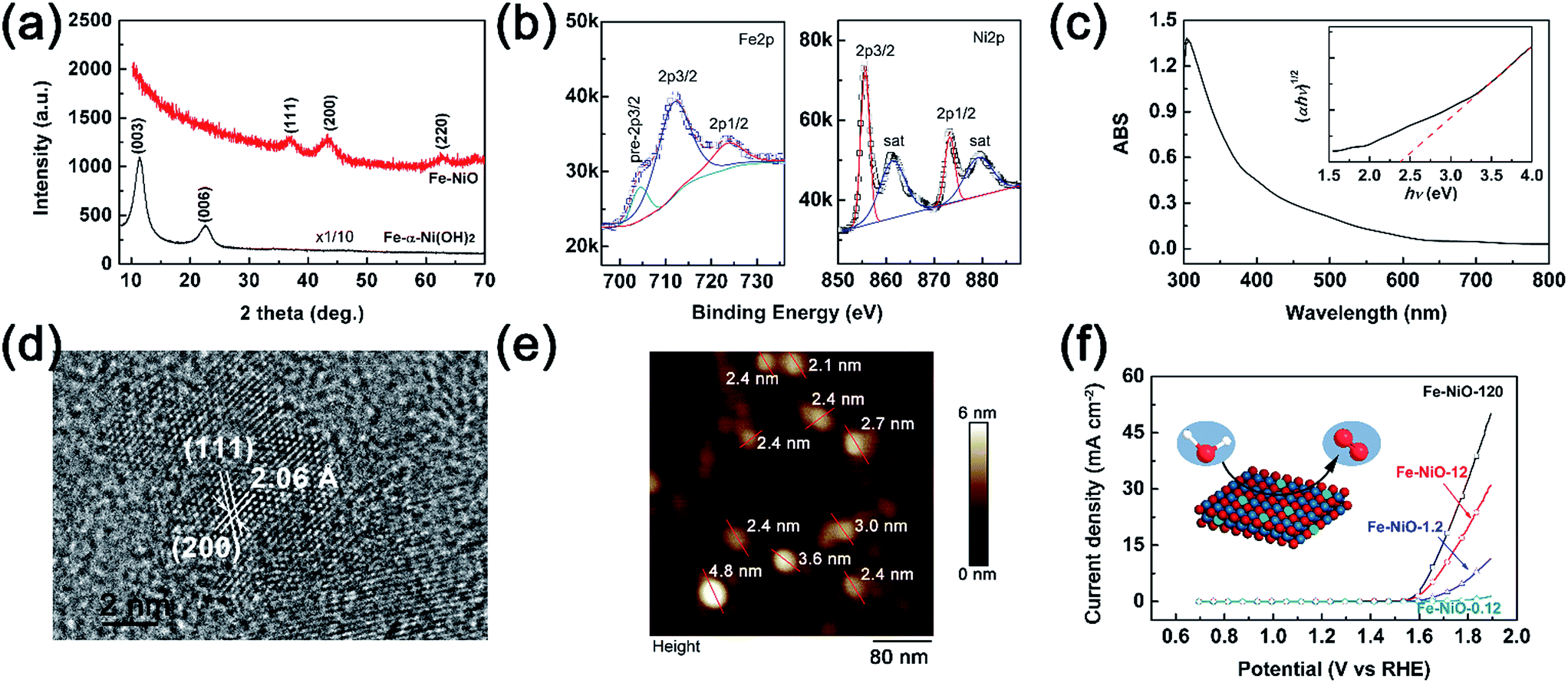 | ||
| Fig. 1 (a) XRD patterns of the Fe-doped Ni(OH)2 precipitate (black curve at bottom) and Fe-doped NiO (red curve on the top); (b) XPS spectra of the Fe-NiO film (left: Fe2p; right: Ni2p); (c) UV-vis absorption spectrum of the Fe-NiO film, the inset was the Tauc plot of indirect band estimation; (d) HR-TEM image of the Fe-NiO nanosheet; (e) AFM height image of the Fe-NiO nanosheets; (f) J–V curves of the Fe-NiO nanosheets on FTO prepared with various concentrations in a 1 M NaOH electrolyte, and a scanning rate of 20 mV s−1. | ||
Thus, the preparation process can be demonstrated through three steps: α-Ni(OH)2 precipitation as in eqn (1), Fe3+ ion exchange in the precipitation as in eqn (2), and thermal dehydration to Fe(3+)-doped NiO in eqn (3):
| Ni2+ + 2OH− → Ni(OH)2 | (1) |
| xFe3+ + Ni(OH)2 + xH2O → FexNi1−x(OH)2+x + xNi2+ + xH+ | (2) |
 | (3) |
For simplicity, we used Fe-NiO to represent the product of FexNi1−xO1+x/2.
The light absorption of the obtained brownish Fe-NiO on FTO was investigated in Fig. 1(c). The sample showed strong absorption between 300 and 550 nm. Using the Tauc plot (inserted in Fig. 1(c)), the indirect light absorption band can be calculated as 2.35 eV. Although the general undoped NiO had a wide bandgap (∼3.6 eV),52 the introduction of Fe dopants resulted in a narrower bandgap due to the less occupation of d-bands of the Fe atoms than the Ni atoms. This observed indirect bandgap coincides with the one calculated by first principles (2.26 eV for 25% doping).53 The high resolution TEM image of the Fe-NiO revealed a highly crystalline structure with the zone axis of [220] in Fig. 1(d), where the lattices separated by 2.06 Å and 2.38 Å were assigned to the (200) and (111) planes, respectively. The angle between these two planes was ca. 54°. Combining the HR-TEM image with the XRD pattern, we expect an ultrathin oriented flake morphology. Then, we prepared a Fe-NiO sample on a Si wafer from a dilute dispersion (1.2 ppm) for thickness evaluation. In Fig. 1(e), the AFM height image displays a typical 2-dimensional morphology with a width of 25–60 nm (size distribution shown in Fig. S2†) and a thickness of 2.1–4.8 nm. Given that the distance between the (220) planes is ca. 1.5 Å, this thickness corresponds to 14–32 layers of nanosheets. When the ultrathin Fe-NiO nanosheets were deposited on the FTO substrate from various concentrations, they all displayed a highly catalytic activity as shown in Fig. 1(f). The current–potential J–V curves showed a dramatic current increase (e.g., 1 mA cm−2) when the applied potential was above 1.57 V (vs. RHE), with the increasing Fe-NiO loading amount. In Fig. S3,† the EDS mapping images of Fe, Ni and O were displayed, showing a uniform distribution of Fe and Ni in the electrocatalyst. Although the exact loading amount of the catalyst on FTO may be not strictly proportional to the content of the solid precursor in the suspension, the electrocatalytic performance showed a positive correlation to the precursor content. Compared with the other OER catalysts, such as NiCoOx, NiOOH, Ni(OH)2, NiFeOx, NiOOH, CoOOH, Co-Pi or NiO,48,54 the overpotential (0.27 V for 0.1 mA cm−2) on ultrathin Fe doped NiO nanosheets is promising for practical OER applications.
The planar Mo-doped bismuth vanadate films were thermally converted from Bi films (40 nm) on the FTO substrate, using VO(acac)2 as the vanadium source and MoO2(acac)2 as the doping precursor in DMSO as reported in the literatures.13 The 2-Mo-BiVO4 film on the FTO substrate was characterized by X-ray powder diffraction using a Cu target. In Fig. 2(a), the peaks marked with red “*” are all ascribed to the diffractions of (011), (112), (004), (121), (006), (204), (301) and (116) on a monoclinic BiVO4 structure (JCPDS card, no. 83-1699). Based on the XRD pattern, the lattice constants (a = 5.177 Å, b = 5.123 Å, c = 11.71 Å and γ = 90.20°) were obtained, which were close to bare and one-step Mo-doped BiVO4 (Fig. S4 and Table S1†). The Mo-doping was additionally confirmed by the Raman and XPS spectra. In Fig. 2(b), the Raman spectrum of Mo-doped BiVO4 displayed identical peaks at 325 cm−1 and 368 cm−1, corresponding to the asymmetric and symmetric bending modes (δas and δs) of the VO43− tetrahedra, respectively.55 And the peaks at 711 cm−1 and 826 cm−1 are assigned to the symmetric and antisymmetric stretching modes (νas and νs) of V–O vibration, respectively.21,55 Both the XRD pattern and Raman spectra revealed that a pure Mo-doped BiVO4 phase was obtained, with no detectable impurities from the other structure or bismuth molybdenites.
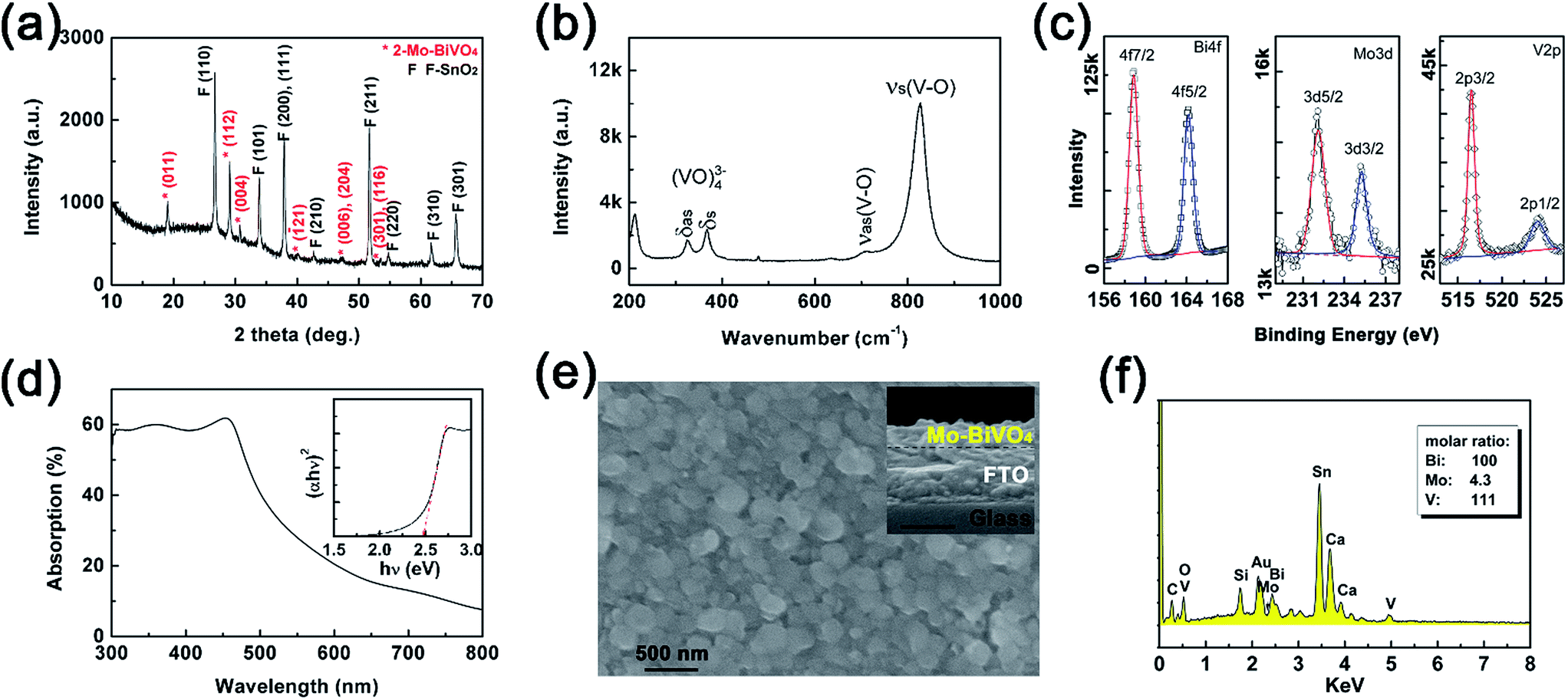 | ||
| Fig. 2 Structure, spectroscopy, morphology and EDS of the 2-Mo-BiVO4 film: (a) XRD pattern of the film on the FTO substrate, where peaks marked with red stars are from Mo-doped BiVO4 and marked with a “F” are from FTO; (b) Raman spectrum excited with the 520 nm laser, the peak at 211 cm−1 was attributed to the external mode of lattice vibration; (c) XPS spectra of Bi4f, Mo3d and V2p of the film; (d) UV-vis absorption spectrum; (e) top view and cross-section (inset) image of the film; (f) EDS spectrum of the film. | ||
The surface oxidation state of 2-Mo-BiVO4 was characterized by the XPS spectra (in Fig. 2(c)). The peaks at 158.9 and 164.2 eV correspond to the Bi4f7/2 and Bi4f5/2 electrons of Bi3+.21 The peaks at 232.1 and 235.25 eV are assigned to the Mo3d5/2 and Mo3d3/2 electrons of Mo6+.56 The peaks at 516.53 and 524.02 eV correspond to V2p3/2 and V2p1/2 electrons of V5+.21 The calculated surface element ratios are 100/5.6/48.9 for Bi/Mo/V, indicating a surface deficiency of V and Mo due to the soaping treatment in alkaline solutions. This is in good agreement with other literature reports.21,57 We also used UV-vis absorption (Fig. 2(d)) to investigate the optical properties, where the band edge absorption was close to 510 nm and the indirect bandgap was ∼2.48 eV as determined by the Tauc plot. From the SEM image in Fig. 2(e), 2-Mo-BiVO4 exhibited a planar morphology, with particle sizes ranging between 200 and 400 nm. From the inset cross-section image, the film showed a rough surface and the thickness was ca. 130 nm. Next, the elements of the film were analysed through EDS (Fig. 2(f)), showing the evidence of Mo, V and Bi from the film with molar ratios of 100/4.3/111 for Bi/Mo/V. The values of the bulk film are higher than those obtained by the XPS surface analysis, presumably due to the larger detect depth through EDS than that through XPS. Thus, the Mo-doped BiVO4 are well prepared with good quality.
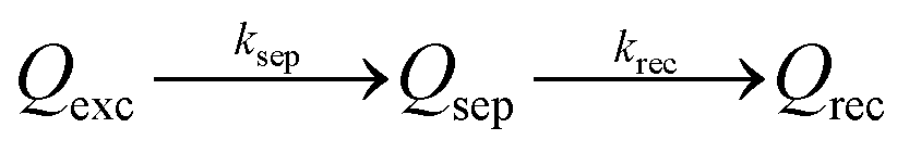
With the well-prepared Fe-doped NiO OER catalyst and Mo-doped BiVO4 semiconductor film, we next studied charge separation, and recombination kinetics on the semiconductor/catalyst interface by transient surface photovoltage spectroscopy (TSPV). Although TSPV has been used for the studies of charge separation in a qualitative fashion, the detailed charge kinetics has rarely been examined in a quantitative manner. The deficiency was partially corrected by our recent study on the Cu-doped CH3NH2PbI3 perovskite film (p-type) with the ITO substrate, where we applied a first-order serial reaction system for the studies of charge separation at the perovskite/air interface.46 Briefly, let us consider a n-type semiconductor as an example. Upon excitation by a laser pulse with nanosecond temporal resolution (Fig. 3(a)), the electron–hole pairs in the conduction and valence bands will be separated to the semiconductor/air interface due to the internal electric field in the Schottky-type junction, which is regarded as the charge separation process. In the absence of an external circuit, ultimately the separated charges will be consumed through a recombination process. The charge separation/recombination processes (Fig. 3(b)) may be expressed as consecutive equations:46
 | (4) |
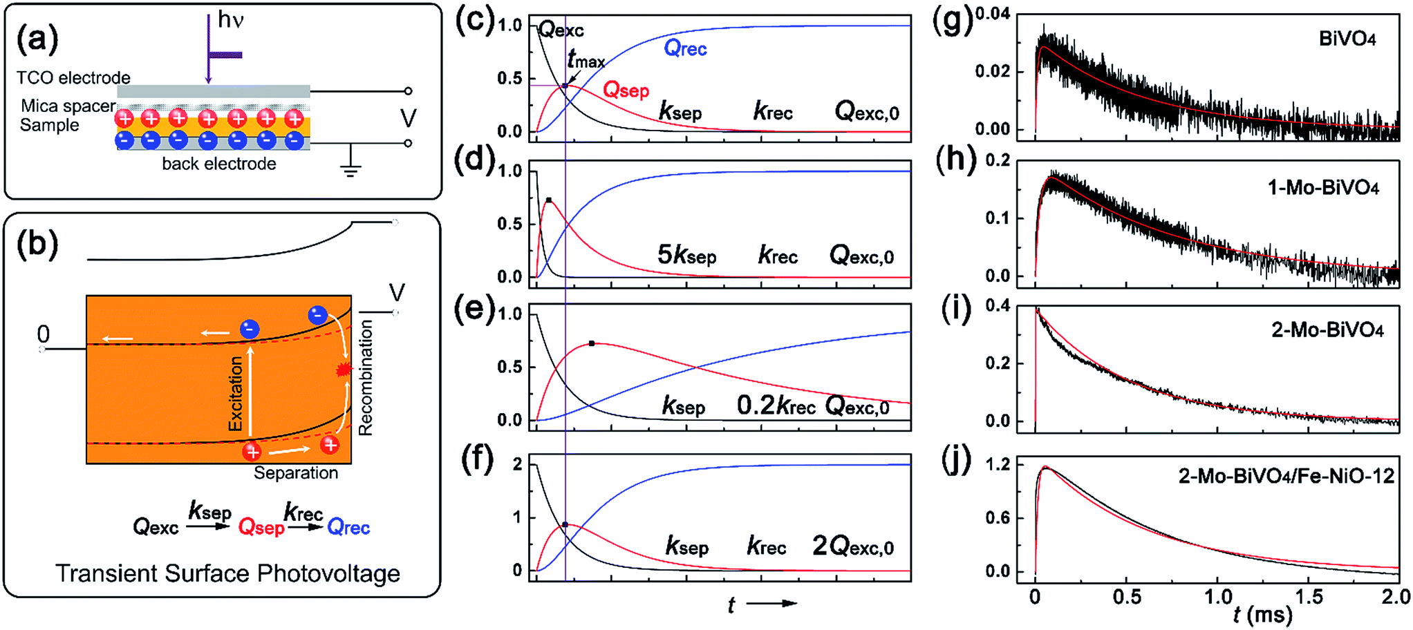 | ||
| Fig. 3 Transient surface photovoltage of the semiconductor films: (a) capacitor-like surface photovoltage measurement configuration; (b) charge kinetics and band structures with light perturbation (red dashed line corresponds to the light conditions); (c)–(f) are the simulated kinetics for excited, separated and recombined charge densities versus time, according eqn (6). ksep, krec and Qexc,0 are the rate constants for charge separation, recombination and the apparent “initially” excited charge density, respectively. (g)–(j) are the experimental (black) and simulated (red) TSPV curves for various bismuth vanadate films of BiVO4, 1-Mo-BiVO4, 2-Mo-BiVO4 and 2-Mo-BiVO4/Fe-NiO-12, respectively. | ||
Since the charge separation (including the diffusion and drift) is sensitive to the initial excited charge pair densities, a first-order charge separation may be applied to describe the separation process (rate constant: ksep). Because the majority charge (electron in n-type semiconductor) density is much higher than the minority charge (hole) density, the recombination is expected to obey a quasi first-order rate law relative to the hole concentration (rate constant: krec). According to the serial first-order reactions theory in physical chemistry,58 the intermediate density (accumulated charge) will display a maximum level at the time of tmax (assuming ksep ≠ krec, other boundary conditions and theoretical calculations can be found in the ESI†):
 | (5) |
 | (6) |
Based on eqn (6), we could simulate the apparent charge densities of the excited pairs (Qexc), separated charge (Qsep) and recombined charge (Qrec), by varying the three parameters of ksep, krec and Qexc,0 (Fig. 3(c)–(f)). When an increase in the charge separation kinetics constant (5 times of ksep in Fig. 3(d)), or a reduction of the charge recombination kinetics constant (0.2 times of krec in Fig. 3(e)) is introduced, an increase of the maximum accumulated charge Qsep,max can be seen, together with a negative or positive shift of tmax, respectively. Alternatively, when hole storage Qexc,0 increases, as shown in Fig. 3(f), the Qsep,max increases, but tmax is unchanged. Therefore, the charge separation or recombination rate constant change can be easily identified through the simulation and/or fitting the TSPV curves.
Next, we obtained the TSPV spectra for doped, undoped BiVO4 films and Fe-NiO modified 2-Mo-BiVO4 films in Fig. 3(g)–(i), respectively. The experimental data (black) were readily fit by simulated ones (red). The maximum separated charge accumulation displayed sensitivity to doping and surface modifications. It was worth noting that the loading amount of the NiO on 2-Mo-BiVO4 was proportional to the solid content of the catalyst precursor using EDS analysis (Fig. S5†). And the SEM and EDS mapping images of the 2-Mo-BiVO4/Fe-NiO-12 were investigated in Fig. S6,† where all the elements were homogenously distributed in the detected region. Moreover, we found the highest Qsep on Fe-NiO modified 2-Mo-BiVO4 films in Fig. 3(j), suggesting a charge storage behavior. The 2-Mo-BiVO4 film exhibited the lowest tmax, indicating a fast charge separation constant. The parameters were shown quantitatively in Table 1. We found that undoped BiVO4 showed a ksep (9.2 × 10⁴ s−1) higher than 1-Mo-BiVO4, while the 2-Mo-BiVO4 had the highest ksep at 2.8 × 10⁶ s−1. We have not found a significant separation enhancement at the 2-Mo-BiVO4/Fe-NiO-12 interface. For the recombination process, there was no apparent difference in the range of 1.35–1.97 × 10³ s−1, and no drastic decrease of rate constant was observed. Interestingly, we noticed that the initial charge pairs (Qexc,0) increased from 0.031 on bare undoped BiVO4, to 0.19 on 1-Mo-BiVO4, 0.39 on 2-Mo-BiVO4 and 1.3 on the 2-Mo-BiVO4/Fe-NiO samples. For the other amount of Fe-NiO loading on the 2-Mo-BiVO4 films, the TSPV signals were in good agreement with the first-order serial reaction kinetic model (Fig. S7†). In addition, we found that a trace amount of Fe-NiO (1.2 ppm dispersion) incorporated into Mo-BiVO4 could significantly increase the Qexc,0 (2.35 in Table S2†), but this surface catalyst reduced the charge separation rate constants. On a thick amorphous NiFeOx layer, we observed two kinetic processes (Fig. S8 and Table S2†): one exhibits fast charge recombination (1.64 × 10⁴ s−1) and large Qexc,0, and the other one features much slower charge recombination (1.50 × 10² s−1) and smaller Qexc,0. This indicates a difference in the mechanism between the ultra-thin crystalline Fe-doped NiO nanosheets and amorphous thick NiFeOx layer. It is worth noting that the consecutive-reaction hypothesis is based on the following assumptions, including high excitation rate and efficiency (∼100%), fast bulk recombination rate and long lifetime (ns–μs) of separated charges. Additionally, for all the TSPV measurements, we used the same laser pulse power (7 μJ per pulse), therefore the theoretical Qexc,0 should be at the same level. It is noted that the calculated initial charge density (Qexc,0) is an apparent value and should be treated as such; it may be compared to the values obtained by transient absorption methods only in a qualitative fashion.34,44 Moreover, the peak height of the separated charge (Qsep,max) on the Fe-doped NiO modified 2-Mo-BiVO4 film displayed 3 times storage as high as that of the bare one (in Table 1). A higher charge separation rate constant could be observed on thinner Fe-NiO application (1.2 or 0.12 samples in Table S2†), which also corresponded to higher accumulated charge densities. Therefore, the increased Qsep,max could be attributed to the “charge storage” effect at the interface.
| Bismuth vanadate film | t max (s) | k sep (s−1) | k rec (s−1) | Q exc,0 (a.u.) | Q sep,max |
|---|---|---|---|---|---|
| a The relative value of the Qexc,0 were shown here (normalized with C as constant 1). | |||||
| BiVO4 | 4.4 × 10⁻⁵ | 9.2 × 10⁴ | 1.74 × 10³ | 0.031 | 0.029 |
| 1-Mo-BiVO4 | 8.6 × 10⁻⁵ | 4.1 × 10⁴ | 1.35 × 10³ | 0.19 | 0.170 |
| 2-Mo-BiVO4 | 2.6 × 10⁻⁶ | 2.8 × 10⁶ | 1.97 × 10³ | 0.39 | 0.385 |
| 2-Mo-BiVO4/Fe-NiO-12 | 5.3 × 10⁻⁵ | 7.2 × 10⁴ | 1.69 × 10³ | 1.30 | 1.17 |
To better understand the reason of these charge separation kinetics, we used the Kelvin probe force microscope (KPFM) to investigate the surface potential under dark conditions and the photoconductivity on bare and Fe-NiO-12 modified 2-Mo-BiVO4 films under ambient conditions. In Fig. 4(a), the height image of the bare 2-Mo-BiVO4 film was shown, with the particle sizes ranging between 150 and 370 nm, consistent with that in the SEM image of Fig. 2(e). When the Fe-NiO-12 was incorporated on the bismuth vanadate surface (Fig. 4(b)), similar particles could be observed with a root-mean-square (RMS) surface roughness factor Rq slightly increased from 19.2 nm to 20.7 nm. By using an Au film (work function of 5.1 eV) as the standard, the surface potential of the Mo-doped BiVO4 films were measured between 4.6 V and 5.2 V vs. vacuum (corresponding to a 0.1 V to 0.7 V vs. NHE). The average surface potential was measured as 4.93 ± 0.09 V (0.43 V vs. NHE), which is slightly higher than the reported conduction band minimum (0.3 V).25 When Fe-NiO was applied onto the surface, the potential (5.03 ± 0.09 V) ranged between 4.7 V and 5.3 V vs. vacuum (0.53 V vs. NHE). This suggests that the surface potential (or work function) of the films are almost the same, due to the extremely low amount of Fe-NiO. Next, the Mott–Schottky method was applied in an electrochemical setting, and 2-Mo-BiVO4 showed a flat band potential of 0.20 V vs. RHE (Fig. S9†). The apparent discrepancy between the Mott–Schottky and Kelvin methods is probably due to the differences in the surface adsorbed species in an electrolyte and in air. It is surprising that the Mott–Schottky slope of the modified sample is higher than that of the bare one. This may be due to the reduced contribution from surface state capacitance. The VFB of Fe-NiO modified 2-Mo-BiVO4 exhibits a negligible shift. For the Fe-doped NiO nanosheets, a negative slope and VFB at 1.41 V vs. RHE was obtained (Fig. S10†), indicating that the Fe-NiO catalyst features holes as the majority carriers. A possible p–n heterojunction between BiVO4 and Fe-NiO would facilitate charge separation at the semiconductor|electrocatalyst interface. We also investigated the electronic conductivity of bare and Fe-NiO-12 modified films, with the back illumination from the FTO side. In Fig. 4(e), the photoconductivity of bare 2-Mo-BiVO4 showed random dark domains (0 to −40 nA). The average areal photocurrent density was estimated to be −1.19 nA, which was 20 times higher than the dark current (−0.060 nA). After Fe-doped NiO was deposited on the 2-Mo-BiVO4 surface, the photocurrent density slightly decreased to −0.69 nA, indicating that the Fe-NiO layer is less conductive than 2-Mo-BiVO4.
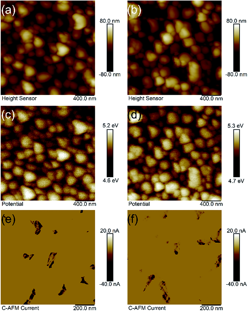 | ||
| Fig. 4 (a), (c) and (e) are the height image, KPFM surface potential topology and photoconductive-AFM of the 2-Mo-BiVO4 films; (b), (d) and (f) are the height image, KPFM surface potential topology and photoconductive AFM of the 2-Mo-BiVO4 coated with the Fe-doped NiO catalyst. The surface potential was calibrated with an Au film (work function at 5.1 ± 0.02 eV). The negative photocurrent in C-AFM corresponds to a positive charge flowing to the probe. | ||
Next, we used photoelectrochemical water splitting to test our understanding that the Fe-NiO nanosheets served as charge reservoirs in the combined system. Different from many other BiVO4 studies which were carried out in phosphate or sulfate solutions, we chose an alkaline solution as the electrolyte because it is widely used in tandem configurations.59 In Fig. 5(a), we compared the photocurrent polarization curves of the undoped BiVO4, doped 1-Mo-BiVO4 and 2-Mo-BiVO4 films. It was found that the bare BiVO4 sample exhibited a poor water oxidation activity (<0.12 mA cm−2 with a positive onset potential at 0.55 V vs. RHE@0.01 mA cm−2). When the Mo dopants were introduced, the photocurrent of 1-Mo-BiVO4 was significantly increased to ca. 0.40 mA cm−2 at 1.4 V, and the onset potential was negatively shifted to 0.27 V. For the 2-Mo-BiVO4 sample, the photocurrent further increased to 0.88 mA cm−2 at 1.4 V and the onset potential remained at 0.27 V. The performance of bare and Mo-doped BiVO4 measured in alkaline solution is among the best of all the reports (Table S3†).31 Moreover, the photoelectrochemical stability of the Mo-doped BiVO4 photoelectrode increased conspicuously with Fe-doped NiO (Fig. S11†), which may be further improved by suitable conformal ALD coating.60 Based on this, we further discussed charge separation and transfer in PEC configuration. The trend of the J–V performance on doped and undoped samples is consistent with the TSPV data: 2-Mo-BiVO4 exhibited better charge separation and larger charge accumulation and, hence, better PEC performance. Next, in Fig. 5(b), when 2-Mo-BiVO4 was chosen as a photoelectrode platform, the ultrathin Fe-doped NiO nanosheets were uniformly dispersed with prolonged ultrasonic treatment and applied onto the bismuth vanadate films. Even with a precursor at 1.2 ppm (which is very low), the photocurrent already increased from 0.15 mA cm−2 to 0.18 mA cm−2 (0.7 V) in the range of 0.5–0.8 V vs. RHE. When the catalyst precursor concentration was increased to 12 ppm, the photocurrent increased dramatically to 0.55 mA cm−2 at 0.7 V and 1.65 mA cm−2 at 1.4 V. The loading amount of Fe-NiO on Mo-BiVO4 was 0.11–0.12 μg cm−2 with the Fe/Ni molar ratio at 0.266/0.734, by re-dissolving in dilute HNO3 and analyzed by ICP-MS. Further increase of the precursor concentrations to 120 ppm led to the decrease of the photocurrent to 1.03 mA cm−2 at 1.4 V. This is possibly due to the increased charge transfer resistance of the less electronically conductive Fe-NiO by the C-AFM measurements, or by the increased charge transfer resistance at the interface.40 Another reason would be increased recombination of the thicker catalyst layers. Although the maximum of the accumulated charge Qsep,max on Mo-BiVO4/Fe-NiO was higher with the Fe-NiO-0.12 or Fe-NiO-1.2 catalyst (in Fig. S7 and Table S2†) than that sample with the Fe-NiO-12 catalyst, extremely thin Fe-NiO-0.12 did not show obvious improvement in the J–V measurements, suggesting that not only the charge storage but also the catalytic sites contributed to the water oxidation reaction. On the other hand, this improvement was also not due to the surface passivation effect. Therefore, when the Fe-NiO modification is used, charge storage, fast kinetics and small transfer impedance need to be balanced consequently.
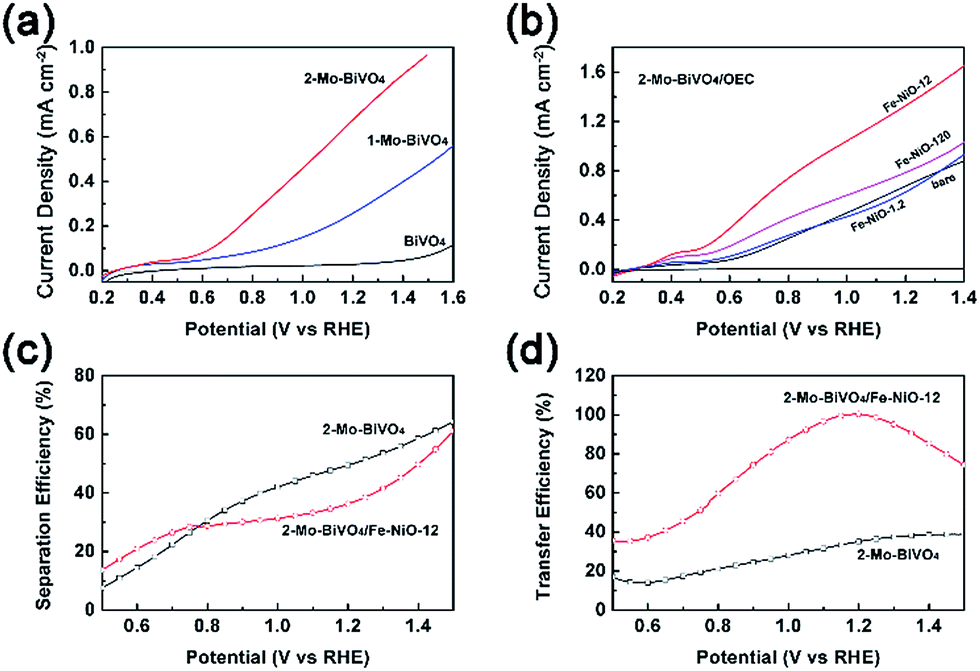 | ||
| Fig. 5 Photocurrent–potential curves for the BiVO4, 1-Mo-BiVO4 and 2-Mo-BiVO4 photoanodes in (a), various Fe-NiO ultrathin nanosheets on the 2-Mo-BiVO4 photoanodes in (b), respectively. The electrolyte was 1 M NaOH and the scanning rate was 20 mV s−1. (c) Charge separation efficiency and (d) charge transfer efficiency of the bare and Fe-NiO modified 2-Mo-BiVO4 photoanodes, respectively. | ||
We then applied charge separation and transfer efficiencies (ηsep and ηtransf) in the electrolyte to verify this speculation. We investigated bare and Fe-NiO-12 modified 2-Mo-BiVO4 sample in the presence of hydrogen peroxide (H2O2 in 1 M NaOH) as a hole scavenger. By comparing the J–V curves (JH2O2) in H2O2 (Fig. S12†) with the theoretical photocurrent (Jabs) by light absorption and 100% IPCE, we estimated the charge separation efficiency (ηsep = JH2O2/Jabs) at the semiconductor|electrolyte interface w/o Fe-NiO catalyst in Fig. 5(c). In the range of 0.5–0.77 V, the charge separation efficiency on 2-Mo-BiVO4/Fe-NiO-12 is higher than on bare 2-Mo-BiVO4. While in the range of 0.77–1.5 V, the charge separation on modified Mo-BiVO4 one is lower than on the bare one. This suggests that better charge separation is expected on 2-Mo-BiVO4/Fe-NiO-12 under the lower band bending conditions (<0.8 V) or slower surface redox reaction rates. The efficiencies of charge transfer to surface water molecules can be evaluated through ηtransf = JOER/JH2O2, assuming that the faradaic efficiencies for water oxidation and H2O2 oxidation are the same. Fig. 5(d) shows a higher charge transfer efficiency for 2-Mo-BiVO4 with the Fe-NiO-12 catalyst than that without. For the bare 2-Mo-BiVO4 sample, the transfer efficiency slightly increased from 13 to 39% (0.5 V to 1.4 V), suggesting over two thirds of the surface accumulated charges may be consumed by the recombination due to the slow water oxidation kinetics. With ultrathin Fe-NiO nanosheets modification, the charge transfer efficiency significantly improved to close to 99% (∼1.2 V). This suggested that the higher applied bias (>0.8 V) contributed more to the surface charge transfer at the Fe-NiO nanosheets-modified Mo-BiVO4 photoanode rather than the charge separation at the Mo-BiVO4 photoanode. The relationship between charge separation and transfer under open circuit and PEC conditions is highly complex. Generally speaking, further increases of charge separation and transfer are of great importance to the PEC performance. And the increased transfer efficiency possibly benefits from the charge storage effect at the semiconductor|electrocatalyst interface.
As we have discussed above, through the TSPV, the Fe-doped NiO ultrathin nanosheet electrocatalyst on the Mo-doped BiVO4 surface displayed a charge storage effect for a better charge separation. Conclusion was obtained by simulations of the kinetics under ambient air conditions without the electrolyte. To further confirm this speculation, we have analysed bare and Fe-NiO-12 modified 2-Mo-BiVO4 photoelectrodes in a 1 M NaOH electrolyte by electrochemical impedance spectroscopy (EIS) at 1.5 V vs. RHE and cyclic voltammetry (CV) between 1.1 and 1.6 V (vs. RHE). In Fig. 6(a) and (c), a typical Nyquist plot of bare 2-Mo-BiVO4 were shown, where the capacitance (CSS) and resistance (RSS) of the surface state were calculated to be 6.42 × 10⁻⁶ F cm−2 and 19.39 Ω cm2, respectively. When the Fe-NiO electrocatalyst was loaded on the 2-Mo-BiVO4 surface, in Fig. 6(b), we used the electrocatalyst to substitute the surface state circuit as Bisquert and Hamann have done for the Co-Pi coated Fe2O3 photoanode.61 The obtained capacitance (Ccat) and resistance (Rcat) of the Fe-NiO catalyst were 2.56 × 10⁻⁵ F cm−2 and 3.98 Ω cm2 (Fig. 6(d)), respectively. The significant increase of Ccat and reduced Rcat was understood as a benefit for charge separation and the overall photoelectrochemical performance. Moreover, the CV curves of the Fe-NiO modified 2-Mo-BiVO4 showed an obvious current density in the window of 1.2–1.6 V vs. RHE (in Fig. S13†), further confirming the surface capacitance behaviour of the Fe-doped NiO electrocatalyst.
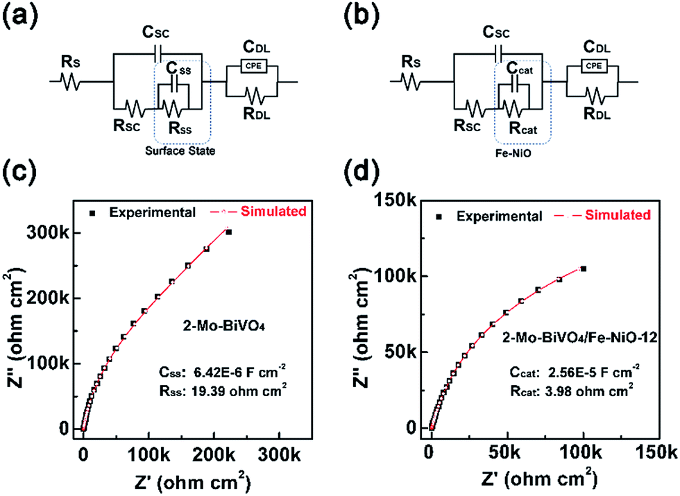 | ||
| Fig. 6 EIS of the bare and Fe-doped NiO modified 2-Mo-BiVO4 photoelectrode measured at 1.5 V vs. RHE in 1 M NaOH under dark conditions: (a) and (c) are the electrochemical equivalent circuit and Nyquist plot of the 2-Mo-BiVO4; (b) and (d) are the electrochemical equivalent circuit and Nyquist plot of 2-Mo-BiVO4/Fe-NiO-12. RS, RSC, CSC, Rcat, and Ccat corresponded to the serial resistance, space charge region resistance, space charge region capacitance, resistance and capacitance from the catalyst, respectively. | ||
Combining the kinetic charge separation/transfer results at the solid/air interface and solid/liquid interface, we gained the following understanding on the charge separation and transfer processes. The p-type Fe-NiO nanosheets at the n-type 2-Mo-BiVO4 surface form an interface that is more complex than a conventional p–n junction as evidenced by the slower charge separation after the Fe-NiO incorporation by TSPV. The increased hole storage at the interface acts as a reservoir possibly due to the Ni2+/Ni3+ pair in the Fe-NiO nanosheets or on the semiconductor side. This surface accumulation of holes induces an internal electric field to impede charge separation, resulting in an apparent slower rate than the bare semiconductor. Moreover, the thicker Fe-NiO nanosheets feature larger resistance/impedance for charge transport. Taken as a whole, we observed relatively low photocurrent on the 2-Mo-BiVO4 film modified with Fe-NiO-120 nanosheets. For comparison, we have also checked thick catalyst layers (e.g., 90 nm), only to observe increased photocurrents during the first scanning. The performance precipitated drastically during the following scans, due to the slow charge transfer to the electrolyte. Interestingly, the ultrathin Fe-NiO layer is permeable to the alkaline electrolyte and possess the fast charge transfer ability. The performance enhancement as observed in our experiments should be attributed to the ultrathin Fe-doped NiO nanosheets. They not only enable relatively high charge transfer efficiencies but also increase charge storage at the interface. Therefore, we understand this phenomena as the “adaptive” behaviours of the ultrathin nanosheets,9 where the photogenerated holes are easily transferred to the redox pairs. By strong contrast, the thick catalyst would form a less “adaptive” junction due to its poor electrical and ionic conductivity, inducing a serious charge recombination and impeding charge transport.6 The band structure is schematically illustrated in Fig. 7(a) and (b). The enhanced water oxidation performance is important evidence for the charge storage function of the ultrathin Fe-doped NiO nanosheets as water oxidation catalysts.
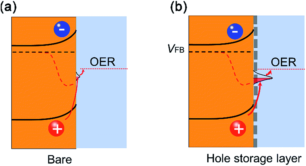 | ||
| Fig. 7 Band structures and charge kinetics on the Mo-doped BiVO4 photoanode with and without ultrathin Fe-NiO nanosheet catalysts: (a) less band bending and smaller split of the quasi-Fermi levels of electrons and holes due to the less minority charge accumulation at the surface; (b) larger band bending and split of the quasi-Fermi levels of the electrons and holes due to the significant accumulation of holes at the surface. | ||
Conclusion
In this work, we have utilized transient surface photovoltage spectroscopy for the investigation of charge kinetics at the semiconductor|electrocatalyst interface. The Mo-doped bismuth vanadate films have been prepared by the conversion of Bi metal films through a two-step reaction. We used the ion-exchange method for the synthesis of ultrathin Fe-doped NiO nanosheets, which could be conveniently applied onto the 2-Mo-BiVO4 films. On the 2-Mo-BiVO4/Fe-NiO samples, we found that charge separation to the surface led to charge accumulation and eventual annihilation following a first-order consecutive reaction mechanism. A charge storage (∼3 times) effect was confirmed on the interface between the ultrathin Fe-NiO nanosheet and the Mo-BiVO4 surface, which significantly enhanced the photoelectrochemical performance. The findings obtained from the planar semiconductor/electrocatalyst system should be easily applied to nanostructured photoelectrodes, which can further increase the photocurrent densities as reported by others.13,14,21 Both the semiconductor|2D electrocatalyst and quantitative transient surface photovoltage analysis may be applied in photoelectrochemistry and other photoelectronic fields for broader impacts.Conflicts of interest
There are no conflicts to declare.Acknowledgements
The authors greatly thank Prof. Dejun Wang from Jilin University for the transient surface photovoltage setup and measurements. This work in Xuchang University is supported by the National Natural Science Foundation of China (Project No. U1604121, 61504117 and 21673200). D. W. is supported by an Ignite Award at Boston College.Notes and references
- N. S. Lewis, Science, 2016, 351, aad1920 CrossRef PubMed.
- R. C. Armstrong, C. Wolfram, K. P. de Jong, R. Gross, N. S. Lewis, B. Boardman, A. J. Ragauskas, K. Ehrhardt-Martinez, G. Crabtree and M. V. Ramana, Nat. Energy, 2016, 1, 15020 CrossRef.
- M. G. Walter, E. L. Warren, J. R. McKone, S. W. Boettcher, Q. Mi, E. A. Santori and N. S. Lewis, Chem. Rev., 2010, 110, 6446–6473 CrossRef CAS PubMed.
- A. Kudo and Y. Miseki, Chem. Soc. Rev., 2009, 38, 253–278 RSC.
- H. Li, Y. Zhou, W. Tu, J. Ye and Z. Zou, Adv. Funct. Mater., 2015, 25, 998–1013 CrossRef CAS.
- P. Tuan Anh, Y. Ping and G. Galli, Nat. Mater., 2017, 16, 401–408 CrossRef PubMed.
- D. R. Gamelin, Nat. Chem., 2012, 4, 965–967 CrossRef CAS PubMed.
- R. Liu, Z. Zheng, J. Spurgeon and X. Yang, Energy Environ. Sci., 2014, 7, 2504–2517 RSC.
- M. R. Nellist, F. A. L. Laskowski, F. D. Lin, T. J. Mills and S. W. Boettcher, Acc. Chem. Res., 2016, 49, 733–740 CrossRef CAS PubMed.
- A. J. Cowan and J. R. Durrant, Chem. Soc. Rev., 2013, 42, 2281–2293 RSC.
- D. Klotz, D. A. Grave and A. Rothschild, Phys. Chem. Chem. Phys., 2017, 19, 20383–20392 RSC.
- Y. Park, K. J. McDonald and K.-S. Choi, Chem. Soc. Rev., 2013, 42, 2321–2337 RSC.
- T. W. Kim and K. S. Choi, Science, 2014, 343, 990–994 CrossRef CAS PubMed.
- Y. Qiu, W. Liu, W. Chen, W. Chen, G. Zhou, P. C. Hsu, R. Zhang, Z. Liang, S. Fan, Y. Zhang and Y. Cui, Sci. Adv., 2016, 2, e1501764 Search PubMed.
- A. Iwase, S. Yoshino, T. Takayama, Y. H. Ng, R. Amal and A. Kudo, J. Am. Chem. Soc., 2016, 138, 10260–10264 CrossRef CAS PubMed.
- S. Gao, B. Gu, X. Jiao, Y. Sun, X. Zu, F. Yang, W. Zhu, C. Wang, Z. Feng, B. Ye and Y. Xie, J. Am. Chem. Soc., 2017, 139, 3438–3445 CrossRef CAS PubMed.
- F. F. Abdi, T. J. Savenije, M. M. May, B. Dam and R. van de Krol, J. Phys. Chem. Lett., 2013, 4, 2752–2757 CrossRef CAS.
- J. A. Seabold and K. S. Choi, J. Am. Chem. Soc., 2012, 134, 2186 CrossRef CAS PubMed.
- H. L. Tan, R. Amal and Y. H. Ng, J. Mater. Chem. A, 2017, 5, 16498–16521 RSC.
- F. F. Abdi, N. Firet and R. v. d. Krol, ChemCatChem, 2013, 5, 490–496 CrossRef CAS.
- V. Nair, C. L. Perkins, Q. Lin and M. Law, Energy Environ. Sci., 2016, 9, 1412–1429 RSC.
- J. W. Jang, D. Friedrich, S. Müller, M. Lamers, H. Hempel, S. Lardhi, Z. Cao, M. Harb, L. Cavallo, R. Heller, R. Eichberger, R. v. d. Krol and F. F. Abdi, Adv. Energy Mater., 2017, 7, 1701536 CrossRef.
- S. Byun, B. Kim, S. Jeon and B. Shin, J. Mater. Chem. A, 2017, 5, 6905–6913 RSC.
- J. Resasco, H. Zhang, N. Kornienko, N. Becknell, H. Lee, J. Guo, A. L. Briseno and P. Yang, ACS Cent. Sci., 2016, 2, 80–88 CrossRef CAS PubMed.
- W. Qiu, Y. Huang, S. Tang, H. Ji and Y. Tong, J. Phys. Chem. C, 2017, 121, 17150–17159 CrossRef CAS.
- E. Y. Liu, J. E. Thorne, Y. He and D. Wang, ACS Appl. Mater. Interfaces, 2017, 9, 22083–22087 CrossRef CAS PubMed.
- B. J. Trzesniewski, I. A. Digdaya, T. Nagaki, S. Ravishankar, I. Herraiz-Cardona, D. A. Vermaas, A. Longo, S. Gimenez and W. A. Smith, Energy Environ. Sci., 2017, 10, 1517–1529 RSC.
- S. Wang, P. Chen, J. H. Yun, Y. Hu and L. Wang, Angew. Chem., Int. Ed., 2017, 56, 8500–8504 CrossRef CAS PubMed.
- M. Chhetri, S. Dey and C. N. R. Rao, ACS Energy Lett., 2017, 2, 1062–1069 CrossRef.
- B. Zhang, L. Wang, Y. Zhang, Y. Ding and Y. Bi, Angew. Chem., Int. Ed., 2018, 57, 2248–2252 CrossRef CAS PubMed.
- M. F. Lichterman, M. R. Shaner, S. G. Handler, B. S. Brunschwig, H. B. Gray, N. S. Lewis and J. M. Spurgeon, J. Phys. Chem. Lett., 2013, 4, 4188–4191 CrossRef CAS.
- F. F. Abdi and R. van de Krol, J. Phys. Chem. C, 2012, 116, 9398–9404 CrossRef CAS.
- D. K. Zhong, S. Choi and D. R. Gamelin, J. Am. Chem. Soc., 2011, 133, 18370–18377 CrossRef CAS PubMed.
- Y. Ma, F. Le Formal, A. Kafizas, S. R. Pendlebury and J. R. Durrant, J. Mater. Chem. A, 2015, 3, 20649–20657 RSC.
- C. Zachaeus, F. F. Abdi, L. M. Peter and R. van de Krol, Chem. Sci., 2017, 8, 3712–3719 RSC.
- M. Long, W. Cai and H. Kisch, J. Phys. Chem. C, 2008, 112, 548–554 CrossRef CAS.
- M. Zhong, T. Hisatomi, Y. Kuang, J. Zhao, M. Liu, A. Iwase, Q. Jia, H. Nishiyama, T. Minegishi, M. Nakabayashi, N. Shibata, R. Niishiro, C. Katayama, H. Shibano, M. Katayama, A. Kudo, T. Yamada and K. Domen, J. Am. Chem. Soc., 2015, 137, 5053–5060 CrossRef CAS PubMed.
- X. Chang, T. Wang, P. Zhang, J. Zhang, A. Li and J. Gong, J. Am. Chem. Soc., 2015, 137, 8356–8359 CrossRef CAS PubMed.
- Y. Liu, Y. Guo, L. T. Schelhas, M. Li and J. W. Ager, J. Phys. Chem. C, 2016, 120, 23449–23457 CrossRef CAS.
- F. Yu, F. Li, T. Yao, J. Du, Y. Liang, Y. Wang, H. Han and L. Sun, ACS Catal., 2017, 7, 1868–1874 CrossRef CAS.
- T. Yao, X. An, H. Han, J. Q. Chen and C. Li, Adv. Energy Mater., 2018, 1800210 CrossRef.
- F. Lin and S. W. Boettcher, Nat. Mater., 2014, 13, 81–86 CrossRef CAS PubMed.
- T. J. Mills, F. Lin and S. W. Boettcher, Phys. Rev. Lett., 2014, 112, 148304 CrossRef PubMed.
- Y. Ma, C. A. Mesa, E. Pastor, A. Kafizas, L. Francàs, F. Le Formal, S. R. Pendlebury and J. R. Durrant, ACS Energy Lett., 2016, 1, 618–623 CrossRef CAS.
- L. Kronik and Y. Shapira, Surf. Sci. Rep., 1999, 37, 1–206 CrossRef CAS.
- K. Lu, Y. Lei, R. Qi, J. Liu, X. Yang, Z. Jia, R. Liu, Y. Xiang and Z. Zheng, J. Mater. Chem. A, 2017, 5, 25211–25219 RSC.
- H. Fan, T. Jiang, H. Li, D. Wang, L. Wang, J. Zhai, D. He, P. Wang and T. Xie, J. Phys. Chem. C, 2012, 116, 2425–2430 CrossRef CAS.
- A. C. Pebley, E. Decolvenaere, T. M. Pollock and M. J. Gordon, Nanoscale, 2017, 9, 15070–15082 RSC.
- S. Li, L. Hou, L. Zhang, L. Chen, Y. Lin, D. Wang and T. Xie, J. Mater. Chem. A, 2015, 3, 17820–17826 RSC.
- Z. Wu, Z. Zou, J. Huang and F. Gao, J. Catal., 2018, 358, 243–252 CrossRef CAS.
- J. A. Dean and N. A. Lange, Lange's Handbook of Chemistry, McGraw-Hill, New York, 1999 Search PubMed.
- M. C. Toroker, D. K. Kanan, N. Alidoust, L. Y. Isseroff, P. Liao and E. A. Carter, Phys. Chem. Chem. Phys., 2011, 13, 16644–16654 RSC.
- J. E. Petersen, F. Twagirayezu, L. M. Scolfaro, P. D. Borges and W. J. Geerts, AIP Adv., 2017, 7, 055711 CrossRef.
- C. C. L. McCrory, S. H. Jung, J. C. Peters and T. F. Jaramillo, J. Am. Chem. Soc., 2013, 135, 16977–16987 CrossRef CAS PubMed.
- V. I. Merupo, S. Velumani, G. Oza, M. Makowska-Janusik and A. Kassiba, Mater. Sci. Semicond. Process., 2015, 31, 618–623 CrossRef CAS.
- C. V. Cáceres, J. L. G. Fierro, J. Lázaro, A. López Agudo and J. Soria, J. Catal., 1990, 122, 113–125 CrossRef.
- F. M. Toma, J. K. Cooper, V. Kunzelmann, M. T. McDowell, J. Yu, D. M. Larson, N. J. Borys, C. Abelyan, J. W. Beeman, K. M. Yu, J. Yang, L. Chen, M. R. Shaner, J. Spurgeon, F. A. Houle, K. A. Persson and I. D. Sharp, Nat. Commun., 2016, 7, 12012 CrossRef PubMed.
- P. Atkins and J. d. Paula, Atkins' Physical Chemistry, W. H. Freeman and Company, New York, 8th edn, 2005 Search PubMed.
- E. Verlage, S. Hu, R. Liu, R. J. R. Jones, K. Sun, C. Xiang, N. S. Lewis and H. A. Atwater, Energy Environ. Sci., 2015, 8, 3166–3172 RSC.
- M. T. McDowell, M. F. Lichterman, J. M. Spurgeon, S. Hu, I. D. Sharp, B. S. Brunschwig and N. S. Lewis, J. Phys. Chem. C, 2014, 118, 19618–19624 CrossRef CAS.
- B. Klahr, S. Gimenez, F. Fabregat-Santiago, J. Bisquert and T. W. Hamann, J. Am. Chem. Soc., 2012, 134, 16693–16700 CrossRef CAS PubMed.
Footnote |
| † Electronic supplementary information (ESI) available. See DOI: 10.1039/c8sc03297a |
| This journal is © The Royal Society of Chemistry 2018 |