
Optical up-conversion devices based on organic and inorganic quantum dot materials
Jing
Xiao
*a,
Zhaoyang
Yin
b,
Zhenyu
Tang
 c,
Zhigang
Gao
a,
Lian
Zhang
a and
Jing
Ren
*d
c,
Zhigang
Gao
a,
Lian
Zhang
a and
Jing
Ren
*d
aCollege of Physics and Electronic Engineering, Taishan University, Taian, Shandong 271000, P. R. China. E-mail: xiaojingzx@163.com
bInstitute of Functional Nano & Soft Materials (FUNSOM), Jiangsu Key Laboratory for Carbon-Based Functional Materials & Devices, Soochow University, Suzhou, Jiangsu 215123, P. R. China
cSchool of Physics, Peking University, Beijing 100871, P. R. China
dKey Laboratory of In-fiber Integrated Optics of Ministry of Education, College of Physics and Optoelectronic Engineering, Harbin Engineering University, Harbin 150001, P. R. China. E-mail: ren.jing@hrbeu.edu.cn
First published on 7th May 2024
Abstract
Infrared (IR) to visible up-conversion devices made by incorporating IR detectors with visible emitting units can directly convert IR light into visible light. They are currently of great significance in engineering monitoring, medical imaging and night vision imaging applications. Up-conversion devices without complex readout circuits can be fabricated entirely using organic or inorganic materials. Additionally, the construction of organic/inorganic hybrid devices has also been accomplished. Strong absorption of IR light and efficient emission of visible light can be achieved by novel IR up-conversion devices based on organic emitting units and inorganic quantum dot photodetectors. Organic/inorganic up-conversion devices act as an effective substitute for the previous infrared imagers that consist of semiconductor photodiode arrays connected with readout circuits. In this review, which is the first of its kind, the characteristics and design principles of up-conversion devices are described. The merits and defects of up-conversion devices with all kinds of semiconductor materials are analysed in a critical way. Finally, the challenges and opportunities encountered by these materials and devices are summarized.
1 Introduction
Infrared (IR) light imaging has been generally applied in optical information and communication technologies.1–3 IR light signals can be captured using photodetectors and then converted into electrical signals. As an indispensable detection part, photodetectors are connected to an imaging display via a complex external circuit.4–6 In recent decades, scientists have been working on optical up-conversion devices, which convert invisible IR light directly into visible light without external circuits.7,8 The optical up-conversion devices consist of detector units and light emitting diodes (LEDs), and are widely applied in night vision systems, infrared cameras, medical equipment, etc.9–11Traditional IR detectors are usually made of III–V compounds or silicon semiconductors, and the IR imaging system is constructed by the combination of a signal amplifier, a readout circuit and a display system.12,13 Although traditional semiconductors play an important role in the field of photodiodes, the fabrication of traditional IR devices is costly due to complex epitaxial growth and lattice matching requirement of compound semiconductors.14,15 Recently, organic/inorganic colloidal quantum dots (CQDs) and organic/inorganic hybrid perovskite semiconductor materials have been used to fabricate high performance up-conversion devices,16–18 which have the characteristics of a simple process and a low cost. They are expected to become an effective substitute for traditional semiconductor devices.19–23
Recently, greatly advanced up-conversion devices of various vertical structures have been reported.24,25 IR photodetectors with high sensitivity and fast-response have been achieved by integrating narrowband sensitive materials, and organic light emitting diodes (OLEDs) have also been acquired with full-color luminosity and high efficiency due to desirable manufacturing benefits.26–28 Color-tunable organic light-emitting displays have been successfully applied to IR visualization.29 Organic devices are usually fabricated by using a vacuum thermal deposition method, and the formation of organic films is not limited by diversified substrates. Thus, flexible and large-area up-conversion devices will be obtained easily.30 Yet the IR detection wavelength of organic materials is still focused on the near-infrared (NIR) range, and is usually limited to 1 μm.31,32 In order to acquire high efficiency up-conversion devices, inorganic detectors integrated with OLEDs are fabricated, due to the dual advantages of inorganic detection performance with organic lighting efficiency.33 High-gain IR-to-visible organic–inorganic up-conversion devices can be integrated with a photon-to-photon conversion efficiency of over 1000%, which is orders of magnitude greater than that of rare-earth ion activated inorganic upconversion materials (∼10%).34
In 2002, the first organic/inorganic up-conversion device integrated with a TiOPc absorber layer and OLEDs was constructed,35 which demonstrated the successful fabrication of an organic/inorganic hybrid. Another organic/inorganic hybrid up-conversion device was fabricated by using an InGaAs/InP IR detector and OLEDs, which was not affected by the lattice matching.33 Novel thin-film devices consist of quantum dots and perovskite semiconductor photodiodes, which have a simpler preparation process and are more cost-effective.36 In 2011, as a hybrid infrared imager, an up-conversion device directly integrated with a PbSe quantum dot IR sensitizer and phosphorescent OLEDs was reported by Kim et al. for the first time. This device can detect IR wavelengths up to 1.5 μm, and its maximum up-conversion efficiency at 1.3 μm is 1.3%.37 Not only has NIR been upconverted to visible light but short-wave IR (SWIR)-to-visible up-conversion devices have also recently appeared with promising results.38,39
IR-to-visible optical imaging systems based on photodetectors and OLEDs can be divided into pixel imaging and pixel-less imaging.40,41 A large number of traditional IR imaging devices are pixelated, and the pixel imaging as a mature imaging method possesses multiple pixel units which are independently arranged in a plane to form a pixel array.42,43 The advantages of the pixel-less scheme are simplification of the device structure and suitability for novel up-conversion devices.44,45
To sum up, organic photodiodes have excellent luminescence performance, but the ability for absorbing IR light is limited. In contrast, inorganic photodiodes can be used as an IR photosensitive layer, but their luminescence efficiency is insufficient. Therefore, a high performance up-conversion device based on OLEDs and inorganic CQD photosensitive units is desirable for IR imaging purposes. In this paper, various designs of organic CQDs and organic/inorganic hybrid up-conversion devices are reviewed with respect to their development and research status. The important up-conversion mechanisms are clarified, and the challenges and prospects of IR up-conversion devices are analyzed. This paper is expected to provide the basic and advanced information to researchers working in this booming field of organic/inorganic hybrid upconversion materials.
2 The mechanism of optical up-conversion devices
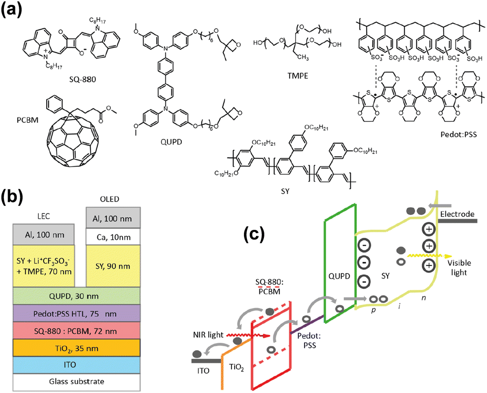
Traditional IR imaging devices consist of IR detectors soldered to a silicon-based readout circuit via an indium column (Fig. 1a).46,47 As the imaging principle declares, IR light is converted into electrical signals, and then the electrical signals are processed to visual images via an external reading circuit and a pictorial display. Therefore, the manufacturing process of this device is very complex.48,49 However, a new conversion device may be achieved comprising of IR detectors and LEDs, and the schematic diagram is shown in Fig. 1b.50 An LED is attached to the top of a photodetector through an intermediate connection layer, which allows the conversion of an IR light signal into photocarriers within the IR-sensitive layer of the detector. After photo-carriers are injected into the LED, the latter converts electrical signals to light signals.51 In this way, IR can be directly converted into visible light without the aid of external circuits so as to simplify the imaging process.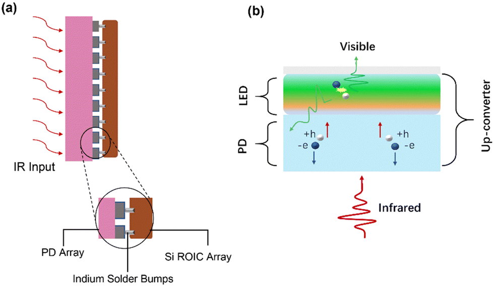 | ||
| Fig. 1 (a) Schematic diagram of the connection between the detector and the reading circuit (infrared input and a Si read out circuit). (b) Schematic diagram of a thin film infrared-to-visible conversion device. | ||
Up-conversion devices consist of two different diodes presented back-to-back as shown in Fig. 2a. Fig. 2b shows various functional layers in typical up-conversion devices. It's hard for holes to overcome the high barrier as holes are resisted at the interface of the anode by the hole-blocking layer. Thus, holes cannot be transferred to the active layer of photodetectors except under a huge reverse bias.52–54 On the other hand, electrons from the cathode cannot be transferred to the anode, and thus an electron-blocking is designed at the interface of the emitting layer to avoid a short circuit. Visible light cannot be emitted from the LED, this is called the off-state (Fig. 2c). A large number of charged carriers are generated under the IR light hitting onto the surface of the detector, and then photocarriers are separated to produce electron current. Photogenerated holes are transferred to the emitting layer and photogenerated electrons are transferred to the anode under the effect of a built-in and external electric field. Therefore, photo-excitation occurs in the emitter layer by combining photogenerated holes and electrons from the cathode, which is called the on-state (Fig. 2d).49,55
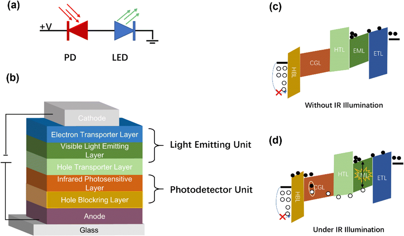 | ||
| Fig. 2 (a) Schematic diagram of photodiodes. (b) Schematic diagram of the up-conversion device structure. (c) and (d) Schematic diagram of the upconverters working without IR (c) and with IR (d) illumination, respectively. | ||
2.1 Photodetector device characterization
The responsivity (R), defined as the ratio of photocurrent to incident light intensity, is used to illustrate the response efficiency of the photodetector to light signals. It is expressed as,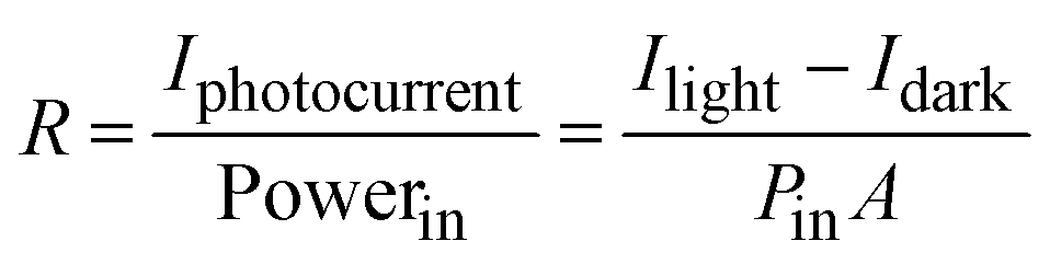 | (1) |
The quantum efficiency (QE) is used to characterize the photon–electron conversion efficiency, which is defined as the probability that an incident photon produces a contribution to the detector current. It is expressed as,
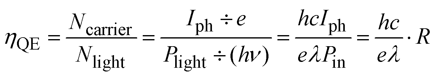 | (2) |
The detectivity (D) is a measure of the signal-to-noise ratio for evaluating the performance of photodetectors, expressed as,
 | (3) |
2.2 Up-conversion device characterization
Up-conversion efficiency, as a key parameter for optical up-conversion devices, refers to the ratio of the number of emitted visible light photons to the number of incident photons. It is expressed as, | (4) |
3 Infrared to visible up-conversion devices
3.1 Organic up-conversion devices
Various organic materials have been used in optical applications that are best known for OLEDs with continuous development of organic electronics.56–58 Some narrow energy gap organic materials were used as IR photosensitive layers because the absorption wavelength reaches 1 μm.59,60 The organic up-conversion devices can be formed by integrating the OLEDs and organic photodetectors,21,61 which were generally designed as a big sandwich structure with a photodetector unit, an intermediate connection layer and a light emitting unit (PD-ICL-LED) (Fig. 2b).62 The structural design of organic up-conversion devices is very flexible, and full-color imaging display can be achieved by selecting peculiar organic materials. The advantages of the organic up-conversion devices are their simplified fabrication process and low cost.63,64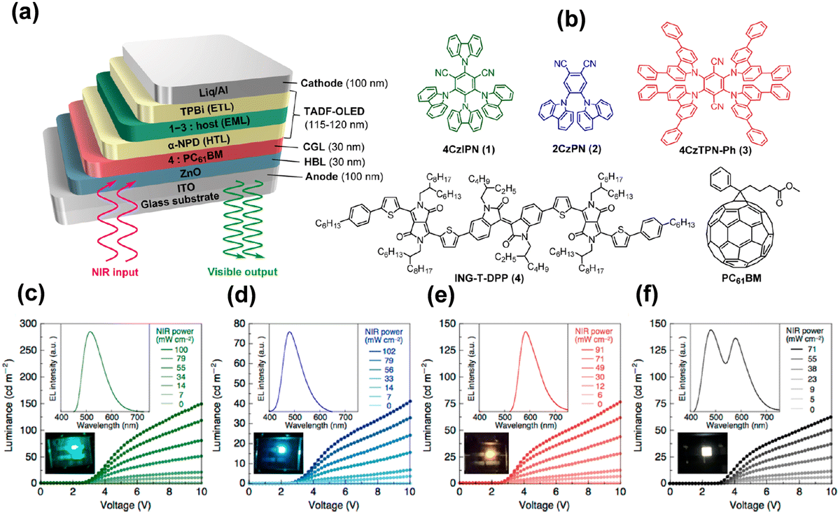 | ||
| Fig. 3 (a) Schematic diagram of the organic up-conversion device based on narrow-band-gap infrared photosensitive materials and TADF-OLEDs. (b) Chemical structures of organic semiconductor materials. (c)–(f) Luminance–voltage characteristics and EL spectra of optical up-conversion devices with an active area of 4 mm2.65 Copyright 2017, American Chemical Society. | ||
According to the structural characteristics of photoelectric imaging systems, it is vital that electrical signals are used for computer processing and machine vision.31,69 Therefore, the applications of both optical imaging and electrical processing have been considered recently. In 2021, an organic up-conversion device with dual optical and electronic reading was reported (Fig. 4a).10 The IR detection wavelength could reach up to 1400 nm, and the visual imaging function was effectively acknowledged in the NIR band. The device structure is shown in Fig. 4d. The organic material 8-hydroxyquinoline aluminum salt (Alq3) was used as the fluorescent emitting layer, and MoO3 as the hole injection layer,70 which was connected with an organic photodetector. Fig. 4c shows the working mechanism of the photocarrier transferring through energy bands under the effect of electric field and IR irradiation in recommended light centers. MoO3 has a low energy position such that its conduction band energy level is close to the highest occupied molecular orbital (HOMO) energy level of NPB acting as an effective hole injection layer.71 Organic photodetector devices based on bulk heterojunctions consisted of a sensitive polymer and a fullerene derivative. The organic bulk heterojunction largely expanded the IR absorption range.72–74 The function of NPB as an interlayer is to upgrade the signal-to-noise ratio of the up-conversion imager, hence the device can provide sensitive electrical signal reading. With a minimum detectable level of light intensity of 1 mW cm−2 for optical reading, the series imager retained similar electronic properties to a single organic photodetector with added benefits of SWIR visualization. The up-conversion efficiency of the device reached 0.15% at 3 V, and the active imaging area was 2 cm2. The device, in addition, encompassed a multitude of application scenarios, including environmental monitoring and pollution detection, as well as optical imaging of tissue samples and tracking biological heartbeat characteristics.
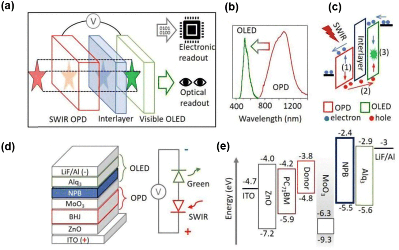 | ||
| Fig. 4 (a) Schematic diagram of imager with dual electronic and optical readouts. (b) Absorption spectrum of OPD and emission spectrum of visible OLED. (c) Working mechanism of upconversion device. (d) Material stacks of the upconversion device and corresponding model of equivalent circuit. (e) Diagram of energy levels.10 Copyright 2021, Wiley-VCH GmbH. | ||
Organic devices can also be fabricated by using solution processes in addition to vacuum thermal evaporation. In 2019, Karen et al. proposed a solution-processed organic up-conversion device (Fig. 5b).75 The IR wavelength of 980 nm was converted to visible yellow light, and photon-to-photon conversion efficiency was around 1.6%. The OLED part in this work was solution processed by using a fluorescent poly copolymer-based material. Recently, high performance color-tunable OLEDs have been reported with rapid progress, which contributes to different ideas of device designs.76
 | ||
| Fig. 5 (a) Organic materials of thin films. (b) Schematic diagram of structure of an all-solution organic device. (c) Organic semiconductor band diagram.75 Copyright 2019, American Chemical Society. | ||
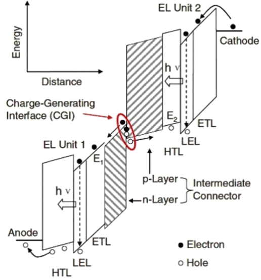 | ||
| Fig. 6 Schematic of vacuum energy levels of each unit of tandem OLEDs.77 Copyright 2016, WILEY-VCH Verlag GmbH. | ||
Lu et al. proposed a novel tandem organic up-conversion device. Fig. 7a shows two structures including a conventional up-conversion device with one emitting unit and a tandem organic up-conversion device with two emitting units.79 The CGL as an IR photosensitive layer was located at the intermediate of the emitting layers, which can detect IR light and transfer photocarriers. Photogenerated carriers can be effectively separated in CGL, and then injected into the upper and lower light emitting units respectively (Fig. 7b).80 The tin(IV) 2,3-naphthalocyanine dichloride, SnNcCl2 was doped in C60 as a photosensitive layer for IR absorption. The photocarriers can be separated and transmitted effectively because the blend of organic materials had several defect states. The up-conversion device could detect IR light at 980 nm which was converted to 520 nm visible with a 4.8% up-conversion efficiency. The device had an excellent closing effect without IR light, (Fig. 7c and d). With the help of the tandem structure, the upconversion efficiency of the device was significantly improved, more than twice that of the control device as shown in Fig. 7e.
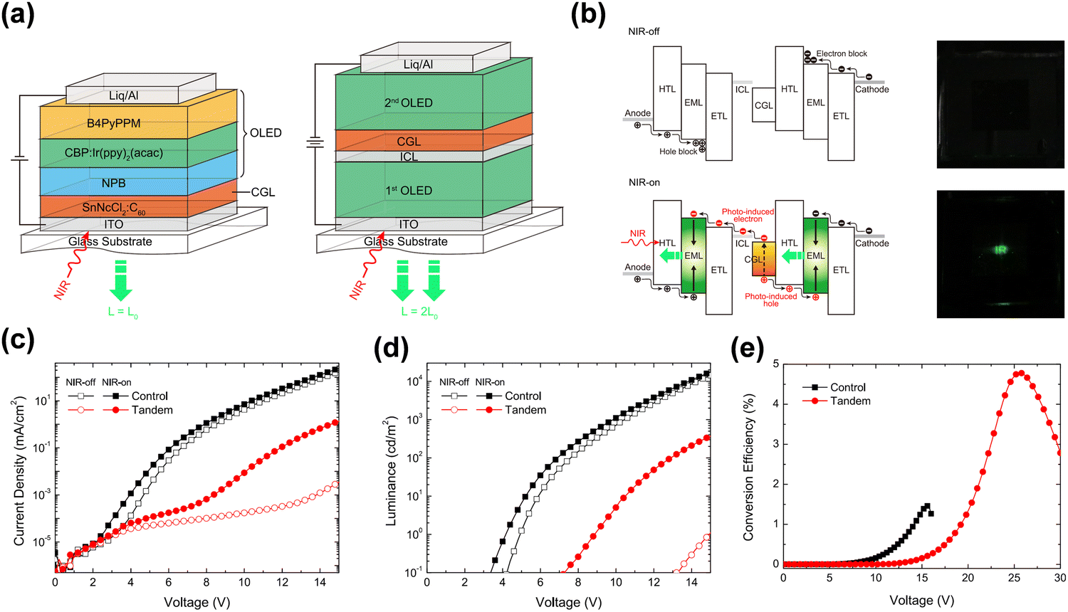 | ||
| Fig. 7 (a) Schematic diagram of structures of the control device and tandem device (single OLED and double OLED). (b) Bandgap diagram of the tandem upconverter and photos of the device operated with and without infrared irradiation. (c) J–V and (d) L–V characteristics. (e) Conversion efficiency diagram.79 Copyright 2018, AIP Publishing. | ||
Another NIR tandem up-conversion device exhibiting an obvious light multiplier effect internally due to tandem OLEDs has proven to be an efficient strategy to enhance luminescence efficiency.81 This work used a narrow band polymer material, which is a blend film consisting of PDPP3T and PCBM. Acting as an active layer of the photodetector, it has strong absorption in the NIR region. Be(pp)2: Ir(ppy)2(acac) acted as the emitting unit and Li2CO3/Al/HAT-CN acted as the CGL of tandem OLEDs, respectively. TAPC acts as the connection layer to integrate up-conversion devices. This device was turned on at 850 nm NIR spectrum. The structures of different up-conversion devices are shown in Fig. 8b. The brightness and current density climb monotonically, reaching saturation at higher voltages under IR irradiation. The rise of saturation brightness and current density is closely related to the input IR power intensity (Fig. 8d). As shown in Fig. 8e, different light emitting units in up-conversion devices cause disparate external quantum efficiency (EQE). The EQE of A1 is obviously higher than those of A2 and A3. It is related to the fact that the photosensitive layer in device A1 can absorb more green light than others, because device A1 provides double brightness when the visible light penetrates through the photosensitive layer. A2 and A3 have the same lighting units, but the device is arranged in the reversed order. The fabrication of A4 device further verifies the contribution of the green emission unit to the EQE of tandem devices.
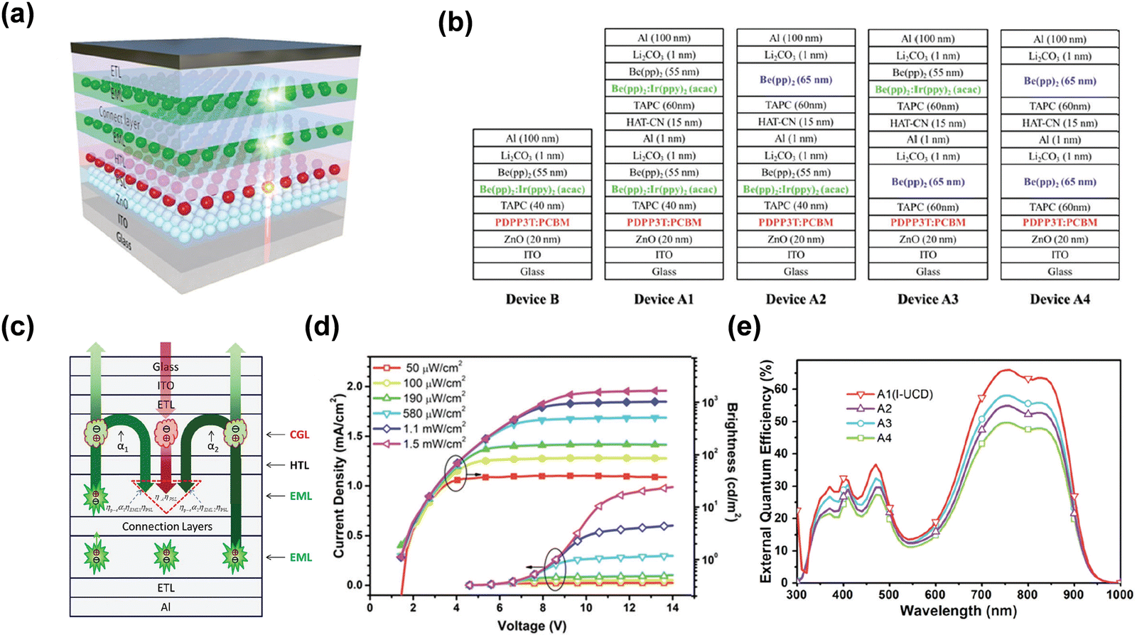 | ||
| Fig. 8 (a) Schematic diagram of the PD with a Tandem OLED up-conversion device. (b) Structures of different up-conversion devices. (c) Schematic diagram of physical processes involved in the device. (d) J–V & B–V characteristics of integrated up-conversion devices under different NIR light powers. (e) EQE spectra of different devices at 9 V bias.81 Copyright 2018, Royal Society of Chemistry. | ||
This series of designs proves the photodetector and photoelectric mutual auxiliary mechanism between OLEDs.82 As visible photons pass through the light-sensitive layer, one part is reabsorbed and the others are transmitted to the outside. The absorbed photons are again converted into photocarriers, and excitations are synthesized repeatedly in the luminescence unit. The total cyclic mechanism is shown in Fig. 8c. These devices based on the tandem OLEDs have higher up-conversion efficiencies. The up-conversion efficiency was as high as 29.6%, being more than twice the efficiency of a single device.
In summary, organic up-conversion devices benefit from the excellent emission performance of OLEDs. However, the detection unit consists of organic materials usually have a limited detection range of wavelength and poor detectivity, thereby constraining their photon-conversion efficiency.
3.2 Inorganic quantum dot up-conversion devices
An inorganic up-conversion device can be fabricated by integrating the inorganic photodetectors with inorganic LEDs.83 Various inorganic QD semiconductor materials have been widely applied in photodiodes by simple solution processes. It has attracted much attention because of their excellent photoelectric properties as zero-dimensional materials. Additional merits include strong absorption in the range of visible and IR and adjustable response wavelength.84–87NIR to visible solution-processed QDs up-conversion devices have been reported.88–90 The up-conversion was successful on two previous different architectures of forward and inverted structures.91,92 Photogenerated electrons and holes were captured respectively as shown in Fig. 9. In these two device structures, the luminescence and detection units are QD materials. Both QDs devices reached fast switching performance. The maximum photon-to-photon conversion efficiency reached over 3% and 6%, respectively. It has saturation luminous intensity work at low voltage bias. These results strongly indicate that the functional layers are competent for the up-conversion process due to their high color saturation, huge sensitivity ability. QD materials are excellent choices for the fabrication of up-conversion devices with simple processes.
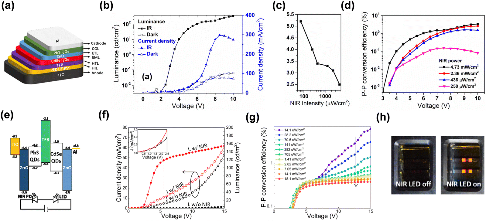 | ||
| Fig. 9 (a) Schematic diagram of device structure. (b), (f) and (g) L–V & J–V characteristic curves. (c) Variation of turn-on voltage with NIR intensity. (d) Up-conversion efficiency. Copyright 2019, AIP Publishing. (e) Semiconductor band diagram. (h) Digital photos of on/off states.91,92 Copyright 2020, The Author(s). | ||
The blocking layer acts as an important part of the up-conversion device, whose function is to limit the charge carrier injection and interface charge generation, also to reduce the influence of noise current. Adding silver ions into the electron transport layer to enhance the tunneling of carriers was an effective strategy reported by Zhou et al. It was different from all previous electron transport layer or hole-blocking layer designs (Fig. 10a).93 High photocurrent was supplied under IR illumination due to the enhancement of tunneling of holes and the capture of photogenerated electrons by Ag nanoparticles (Ag NPs), as well as the efficient combination of the photogenerated holes and cathode electrons in the light emitting region. The device also achieved high saturation light intensity and bright green light emission at low reverse bias (Fig. 10c and e).
 | ||
| Fig. 10 (a) Schematic diagram of device structure and infrared to visible light conversion mechanism. (b) Absorption spectrum of QDs. (c) L–V characteristic curves. (d) Up-conversion efficiency. (e) Schematic of on/off states.93 Copyright 2020, SpringerNature. | ||
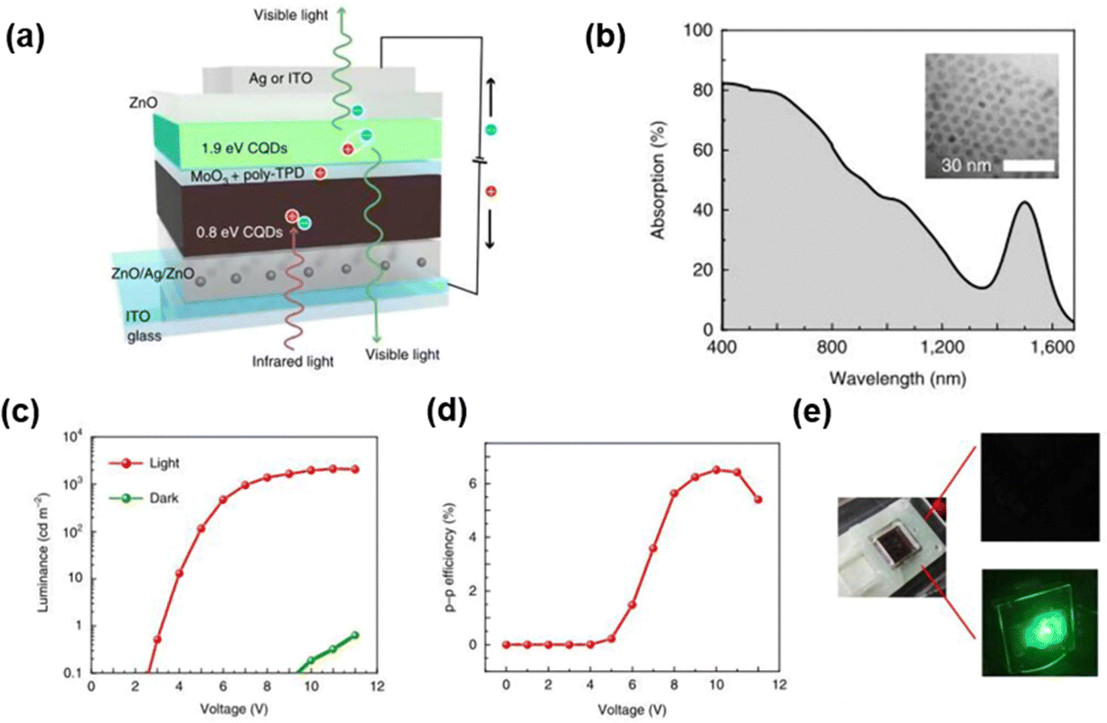
A photodetector absorption layer of PbS CQDs integrated with a light-emitting diode layer of CdSe/ZnS CQDs was achieved by solution-process, and the combination of MoO3/poly-TPD was used as the interface connection layer for the first time. This up-conversion device possesses a high NIR light to visible conversion efficiency of 6.5% and a low turn-on voltage of 2.5 V. Additionally, the photodetector can be integrated with flexible substrates. As for all CQDs devices, it is a promising candidate for low-cost and flexible photodiodes. However, the key of multilayer solution treatment is that the latter layer structure is selectively prepared on the basis of the solvent used in the previous layer, which limits the fabrication of QDs luminescence layer. Besides, a large number of defects in the QDs films are also adverse for the luminescence efficiency.94–97
3.3 Inorganic PDs & OLED up-conversion devices
Inorganic QDs detectors integrated OLEDs have been reported as an effective combination strategy for NIR imagers, and appeared to be a solution to the questions of the early photodetector imaging devices.45,98 In previous studies, inorganic PIN photodiodes and inorganic quantum well photodiodes with OLEDs have achieved successful up-conversion phenomena. However, the fabrication of detectors requires complex epitaxial growth and large-area application is unideal.99,100 Therefore, the up-conversion devices integrated with QDs detector and OLEDs came into being. Inorganic QDs materials were used as the photosensitive layer of up-conversion devices due to their excellent properties and simple processes.In 2011, Kim et al. reported a hybrid up-conversion device by integrating a PbSe nanocrystal NIR layer with OLEDs, which has an IR sensitivity to 1.5 μm and an up-conversion efficiency of 1.3% (Fig. 11a, d and e).37,101 The important role of ZnO as the hole-blocking layer was clearly proved by comparing devices with and without the ZnO layer (Fig. 11c). The absorption wavelength was controlled by adjusting the size of the QDs (Fig. 11b).102,103 Although the conversion efficiency was low, it initiated a novel idea for the combination of QDs and OLEDs and created an innovative platform for organic/inorganic hybrid devices.
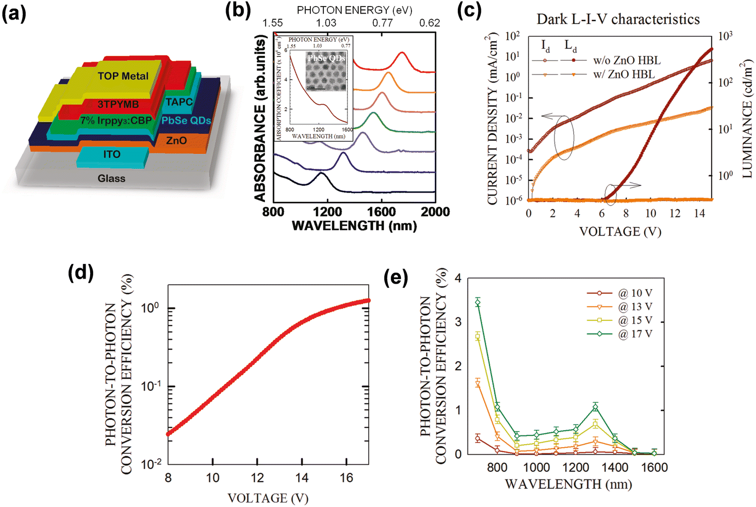 | ||
| Fig. 11 (a) Schematic diagram of device structure. (b) Absorption spectra of various QDs. (c) Dark L–I–V characteristic curves. (d) and (e) Up-conversion efficiency.37 Copyright 2011, American Chemical Society. | ||
However, it is difficult to obtain a high efficiency up-conversion device by simply integrating a photodetector with OLEDs.50,104,105 Yu et al. reported that a high-gain IR-to-visible up-conversion device which consists of a QDs photodetector and OLEDs by connecting a phototransistor.34 It achieved an up-conversion efficiency over 1000% and a faster response speed, which can be ascribed to integration of a vertical phototransistor between the photodetector and OLEDs, the device structure diagram is shown in Fig. 12a. A perforated porous ITO film as a source electrode is shown in Fig. 12c.
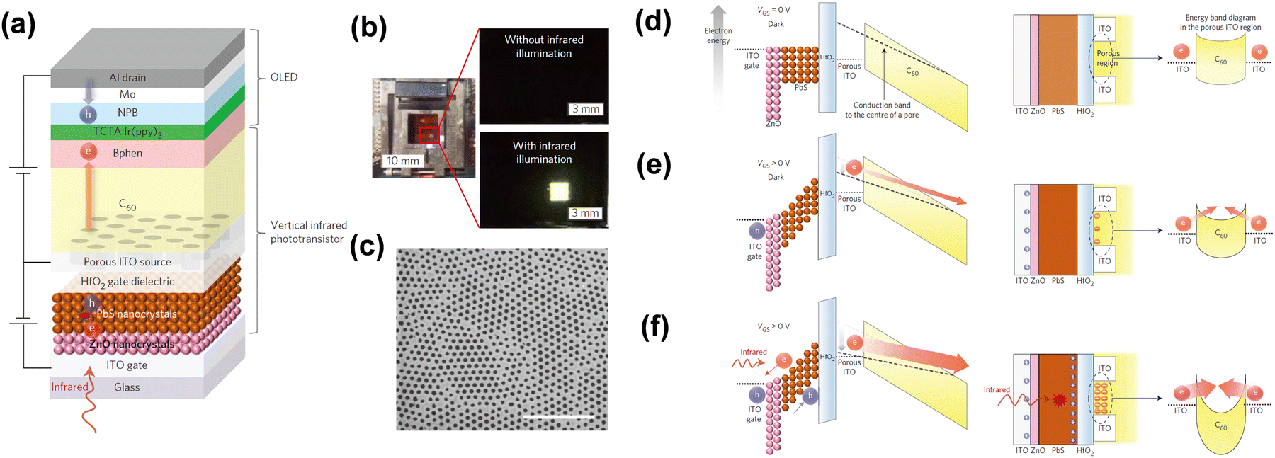 | ||
| Fig. 12 (a) Schematic diagram of device structure. (b) Photos of on/off states. (c) SEM image of the porous ITO film. (d), (e) and (f) Schematic diagram of physical mechanisms.34 Copyright 2016, Springer Nature. | ||
A three-terminal device was proposed consisting of a photodetector, a transistor and OLEDs. This device has a high photon to electron efficiency and the current through the OLEDs can be modulated. During the device operation, IR photons passed through the ITO gate electrode to the PbS active layer and generated photocarriers. Electrons from the ITO source electrode injected into OLEDs through the C60 channel layer to achieve emitting. Fig. 12b shows the device work states with and without IR illumination. Fig. 12d shows the band diagrams to explain the physical mechanism of the vertical up-conversion device at work-off state. Under the device work-on state, the photogenerated carriers stacked at the surface of HfO2 dielectric layer, and the function of the transistor was embodied. The electrons in C60 gradually increased, and the high photoelectric gain was reflected (Fig. 12f).
To summarize, hybrid up-conversion devices that integrate inorganic PDs and OLEDs can leverage the exceptional detectivity of inorganic PDs and the excellent emission capability of OLEDs. These devices exhibit a broad range of infrared detection wavelengths and high quantum efficiency, making them highly desirable for up-conversion applications.
4 Conclusions and outlook
Up-conversion devices composed of organic and inorganic CQDs materials are emphatically exemplified. The performance and structure characteristics of these devices are introduced. IR up-conversion devices are proposed to reduce the IR imaging cost and improve imaging efficiency. Their performance has been continuously improved, with the IR-to-visible up-conversion efficiency significantly updated. Most of the reports published so far are summarized in Table 1.| Device structure | λ NIR (nm) | λ Vis (nm) | L max (cd m−2) | η p–p (%) | Ref. | ||
|---|---|---|---|---|---|---|---|
| All-organic devices | 1 | ITO/PVK:TNFDM/Alq3/Mg:Ag/Ag | 810 | 530 | — | — | 61 |
| 2 | ITO/SnPc:C60/TAPC/Irppy3:CBP/3TPYMB/LiF/Al | 890 | 525 | 853@15 V | 2.7 | 21 | |
| 3 | ITO/ClAlPc:C70/TAPC/CBP:Ir(ppy)3/Bphen/LiF/Al | 780 | 525 | 1553@7 V | 6 | 63 | |
| 4 | ITO/ZnO/ING-T-DPP:PCBM/α-NPD/TADF-OLEDs (R,B,G)/TPBi/Liq/Al | 810 | 512, 480, 584 | 75, 150, 45@10 V | 0.11, 0.04, 0.07 | 65 | |
| 5 | ITO/NPB/CBP:Ir(ppy)2(acac)/B4PyPPM/Liq/Al/NPB/CBP:Ir(ppy)2(acac)/B4PyPPM/Liq/Al | 980 | 520 | 124@6 V | 4.8 | 79 | |
| 6 | ITO/C60:PbPc/NPB/TADF-DPEPO/2PXZ-OXD/Bphen/LiF/Al | 808 | 530 | 103@15 V | Over 100 | 69 | |
| 7 | ITO/TiO2/SQ-88O:PCBM/MoO3/TPD/Alq3/Ca (10 nm)/Al (100 nm) or Ca (2 nm)/Au (8 nm)/Alq3 | 980 | 540 | 313@10 V | 0.27 | 31 | |
| 8 | ITO/ZnO/PDPP3T:PCBM/TAPC/Be(pp)2:Ir(ppy)2(acac)/Be(pp)2/Li2CO3/Al/HAT-CN/TAPC/Be(pp)2/Li2CO3/Al | 850 | 520 | 1504@12 V | 29.6 | 81 | |
| 9 | ITO/TiO2/C60:Cy7-T/MoO3/β-NPB/Alq3/LiF/Al | 830 | 540 | 14@10 V | — | 72 | |
| 10 | ITO/TiO2/SQ-88O:PCBM/Pedot:PSS/QUPD/SY/Ca/Al | 980 | 575 | 760@7.5 V | 1.6 | 75 | |
| 11 | ITO/ZnO/PBDTT-BTQ:PCBM/m-MTDATA/TAPC/CBP:Ir(ppy)3/TPBi/LiF/Al | 1000 | 520 | 7 @12 V | 0.8 | 59 | |
| 12 | ZnO/PCBM:donor/MoO3/NPB/Alq3/LiF/Al | 940 | 520 | ∼102 | 0.15 | 10 | |
| All-inorganic devices | 13 | ITO/ZnO/HgTe CQDs/Ag2Te CQDs/PEDOT:PSS/TFB/CdSe@ZnS CQDs/ZnMgO/Ag | 520 | 500@15 V | 10 | 38 | |
| 14 | ITO/PEDOT:PSS/TFB/CdSe QDs/ZnO/PbS QDs/Al | 970 | 624 | 330@10 V | 3.35 | 91 | |
| 15 | ITO/ZnO/PbS QDs/TFB/CdSe QDs/ZnO/Al | 970 | 624 | 155@15 V | 6.3 | 92 | |
| 16 | ITO/ZnO/Ag/ZnO/PbS QDs/MoO3/CQDs/ZnO/Ag or ITO | 940 | 520 | 2100@12 V | 6.5 | 93 | |
| Inorganic PDs & OLEDs devices | 17 | n-Si/ITO/NPB/CBP:Ir(ppy)3/TPBi/LiF/Al | 900 | 473, 514, 544 | 102@20 V | 9.2 | 30 |
| 18 | Au/n-Ge/ITO/NPB/CBP:Ir(ppy)3/TPBi/LiF/Al | 1880 | 526 | — | 7 | 39 | |
| 19 | n-InP/InGaAs/p-InP/C60/CuPc/NPB/Alq3:C545T/Alq3/LiF/Al/Ag | 1500 | 520 | 1580@11.5 V | 1.5 | 106 | |
| 20 | InGaAs/InP p-n-p-HPT/C60/CuPc/α-NPD/Alq3:C545T/Alq3/LiF/Al/Ag | 1500 | 564 | — | 59 | 50 | |
| 21 | InGaAs/Gas 30-QWs/MoO3:CuPc/NPB/C545T:Alq3/Alq3/LiF/Al | 980 | 520 | 1264@20 V | 0.81 | 49 | |
| 22 | ITO/ZnO/PbSe QD/TAPC/CBP:Ir(ppy)3/3TPYMB/Al | 1300 | 520 | 8@15 V | 1.3 | 37 | |
| 23 | InGaAs/Gas 60-QWs/MoO3:CuPc/NPB/C545T:Alq3/Alq3/LiF/Al | 930 | 520 | 6050@20 V | 4 | 100 | |
| 24 | ITO/n-GaAs/InGaAs QWs/p-GaAs/MoO3/NPB/CBP:Ir(ppy)3/BCP/Alq3/LiF/Al | 980 | 510 | 7900@15 V | 4.8 | 99 | |
| 25 | ITO/ZnO/PbS QD/HfO2/porous ITO/C60/Bphen/TCTA:Ir(ppy)3/NPB/Mo/Al | 1042 | 520 | — | 1591 | 34 |
As the early type of up-conversion devices, PIN and quantum well photodetectors integrated OLEDs were made of III–V compound semiconductors or other traditional semiconductor materials. Although their infrared detection wavelength can exceed 1.5 μm, their work voltage is very high and the lattice matching needs to be considered during the preparation process. Organic materials usually have the characteristics of an amorphous structure, so their preparation process is not limited by lattice matching requirement and it can be readily deposited on arbitrary substrates by a simple vacuum coating method. Additionally, tandem OLEDs as high efficiency emitting devices are used as a promising candidate in up-conversion devices. However, the IR wavelength detection boundary is barely satisfactory because of the limitation of organic semiconductor bandgaps. By contrast, the novel design by combining organic and inorganic materials appear to be more popular. Inorganic QD materials have multiple advantages; one of the key properties is that their absorption bands can be readily adjusted. They can be prepared by a simple solution process and have lower costs. Theoretically, the up-conversion devices integrating inorganic QDs and OLEDs can reflect the common advantages of both, and PD-OLEDs can achieve efficiency pixel-less imaging. The up-conversion devices based on QD photodiodes and OLEDs can continue to develop with the rapid progress of QD and OLED semiconductor materials.
So far, the IR-to-visible conversion efficiency of up-conversion devices is still below expectation, which can be attributed to the weak signal of IR emissions, as well as problems in the optical–electrical–optical signal conversion process, such as carrier transport influenced by carrier traps and defect states. In order to obtain high performance up-conversion devices, the high responsivity of photodiodes is of paramount importance. The potential solutions involve utilizing triode tubes to amplify the signal or employing tandem device structures to optimize the quantum efficiency. Besides, the interface of semiconductor films and charge connection with gain structures need to be considered, by capitalizing on the mature theory of metal–semiconductor, inorganic and organic semiconductor interfaces. The top electrode of up-conversion devices can be considered as a transparent electrode to improve the ability of IR to visible light detection. Moreover, phosphorescent OLEDs and TADF-OLEDs with higher external quantum efficiencies are very favorable as the emitting units, and the IR absorption wavelength needs to be further pushed into the middle- and far-IR range.
There is still significant work to be accomplished prior to the commercialization of up-conversion devices, potential challenges are anticipated during array or pixelated preparation owing to the complex lithography and cleaning procedures associated with handling and preparing multi-layered inorganic and organic films. These challenges could result in suboptimal yields for large-scale production. Furthermore, practical applications necessitate additional improvements in both device efficiency and long-term operational stability.
Author contributions
J. X., Z. Y., Z. T., Z. G., and L. Z. performed references analysis and manuscript writing; J. X., and J. R. organized and inspect the manuscript.Conflicts of interest
There are no conflicts to declare.Acknowledgements
This work was financially supported by the National Natural Science Foundation of China (No. 62374112 and 62305244) and the Natural Science Foundation of Shandong Province (No. ZR2022MF271 and ZR2021QE060).References
- S. Goossens, G. Navickaite, C. Monasterio, S. Gupta, J. J. Piqueras, R. Perez, G. Burwell, I. Nikitskiy, T. Lasanta, T. Galan, E. Puma, A. Centeno, A. Pesquera, A. Zurutuza, G. Konstantatos and F. Koppens, Nat. Photonics, 2017, 11, 366–371 CrossRef CAS.
- J. H. Koo, S. Jeong, H. J. Shim, D. Son, J. Kim, D. C. Kim, S. Choi, J. I. Hong and D. H. Kim, ACS Nano, 2017, 11, 10032–10041 CrossRef CAS PubMed.
- X. Gao, Y. Cui, R. M. Levenson, L. W. Chung and S. Nie, Nat. Biotechnol., 2004, 22, 969–976 CrossRef CAS PubMed.
- Y. Fang and J. Huang, Adv. Mater., 2015, 27, 2804–2810 CrossRef CAS PubMed.
- B. R. Sutherland, A. K. Johnston, A. H. Ip, J. X. Xu, V. Adinolfi, P. Kanjanaboos and E. H. Sargent, ACS Photonics, 2015, 2, 1117–1123 Search PubMed.
- Q. Chen, N. De Marco, Y. Yang, T. B. Song, C. C. Chen, H. X. Zhao, Z. R. Hong, H. P. Zhou and Y. Yang, Nano Today, 2015, 10, 355–396 CrossRef CAS.
- A. Zampetti, A. Minotto and F. Cacialli, Adv. Funct. Mater., 2019, 29, 1807623 CrossRef.
- L. Liang, D. B. L. Teh, N. D. Dinh, W. Chen, Q. Chen, Y. Wu, S. Chowdhury, A. Yamanaka, T. C. Sum, C. H. Chen, N. V. Thakor, A. H. All and X. Liu, Nat. Commun., 2019, 10, 1–9 CrossRef CAS PubMed.
- A. P. H. J. S. Sandhu, B. W. Alphenaar and J. R. A. Cleaver, Appl. Phys. Lett., 2000, 76, 1507–1509 CrossRef.
- N. Li, N. Eedugurala, D. S. Leem, J. D. Azoulay and T. N. Ng, Adv. Funct. Mater., 2021, 31, 2100565 CrossRef CAS.
- J. E. Kallhammer, Nat. Photonics, 2006, 12–13 CrossRef.
- M. R. Olson, K. J. Russell, V. Narayanamurti, J. M. Olson and I. Appelbaum, Appl. Phys. Lett., 2006, 88, 161108 CrossRef.
- J. Chen, J. Tao, D. Ban, M. G. Helander, Z. Wang, J. Qiu and Z. Lu, Adv. Mater., 2012, 24, 3138–3142 CrossRef CAS PubMed.
- Y. Yang, W. Z. Shen, H. C. Liu, S. R. Laframboise, S. Wicaksono, S. F. Yoon and K. H. Tan, Appl. Phys. Lett., 2009, 94, 093504 CrossRef.
- H. Cansizoglu, A. F. Elrefaie, C. Bartolo-Perez, T. Yamada, Y. Gao, A. S. Mayet, M. F. Cansizoglu, E. P. Devine, S. Y. Wang and M. S. Islam, IEEE Trans. Electron Devices, 2018, 65, 382–391 CAS.
- Z. Xu, Z. Huang, C. Li, T. Huang, F. A. Evangelista, M. L. Tang and T. Lian, ACS Appl. Mater. Interfaces, 2020, 12, 36558–36567 CrossRef CAS PubMed.
- M. C. Melquíades, R. Aderne, A. Cuin, W. G. Quirino, M. Cremona and C. Legnani, Opt. Mater., 2017, 69, 54–60 CrossRef.
- N. Li, Y. S. Lau, Z. Xiao, L. M. Ding and F. R. Zhu, Adv. Opt. Mater., 2018, 6, 1801084 CrossRef.
- X. T. Yin, C. Zhang, Y. X. Guo, Y. W. Yang, Y. L. Xing and W. X. Que, J. Mater. Chem. C, 2021, 9, 417–438 RSC.
- A. H. Ip, A. Kiani, I. J. Kramer, O. Voznyy, H. F. Movahed, L. Levina, M. M. Adachi, S. Hoogland and E. H. Sargent, ACS Nano, 2015, 9, 8833–8842 CrossRef CAS PubMed.
- D. Y. Kim, D. W. Song, N. Chopra, P. De Somer and F. So, Adv. Mater., 2010, 22, 2260–2263 CrossRef CAS PubMed.
- T. Kim, E. Palmiano, R. Z. Liang, H. Hu, B. Murali, A. R. Kirmani, Y. Firdaus, Y. Gao, A. Sheikh, M. Yuan, O. F. Mohammed, S. Hoogland, P. M. Beaujuge, E. H. Sargent and A. Amassian, Appl. Phys. Lett., 2017, 110, 223903 CrossRef PubMed.
- P. Guyot-Sionnest, M. M. Ackerman and X. Tang, J. Appl. Phys., 2019, 151, 0609011 Search PubMed.
- T. Rao, M. Chen, G. Mu and X. Tang, Coatings, 2022, 12, 456 CrossRef CAS.
- T. Rao, Y. Xu, X. Tang and G. Mu, ACS Appl. Nano Mater., 2024, 7, 904–918 CrossRef CAS.
- X. Y. Zhu, Y. H. Li, Z. L. Wu, C. W. Lin, D. G. Ma, Z. J. Zhao and B. Z. Tang, J. Mater. Chem. C, 2021, 9, 5198–5205 RSC.
- M. Wu, T. A. Lin, J. O. Tiepelt, V. Bulovic and M. A. Baldo, Nano Lett., 2021, 21, 1011–1016 CrossRef CAS PubMed.
- K. Xu, X. Xiao, W. Zhou, X. Jiang, Q. Wei, H. Chen, Z. Deng, J. Huang, B. Chen and Z. Ning, ACS Appl. Mater. Interfaces, 2020, 12, 15414–15421 CrossRef CAS PubMed.
- G. Mu, T. Rao, Y. Qi, S. Ma, Q. Hao, M. Chen and X. Tang, Adv. Funct. Mater., 2023, 33, 2301280 Search PubMed.
- T. Rao, Q. Hao, G. Mu, T. Qin, Y. Tan, P. Zhao, D. Kong, M. Chen and X. Tang, APL Photonics, 2023, 8, 036106 CrossRef CAS.
- K. Strassel, A. Kaiser, S. Jenatsch, A. C. Veron, S. B. Anantharaman, E. Hack, M. Diethelm, F. Nuesch, R. Aderne, C. Legnani, S. Yakunin, M. Cremona and R. Hany, ACS Appl. Mater. Interfaces, 2018, 10, 11063–11069 CrossRef CAS PubMed.
- S. Gielen, C. Kaiser, F. Verstraeten, J. Kublitski, J. Benduhn, D. Spoltore, P. Verstappen, W. Maes, P. Meredith, A. Armin and K. Vandewal, Adv. Mater., 2020, 32, e2003818 CrossRef PubMed.
- D. Ban, S. Han, Z. H. Lu, T. Oogarah, A. J. SpringThorpe and H. C. Liu, Appl. Phys. Lett., 2007, 90, 093108 CrossRef.
- H. Yu, D. Kim, J. Lee, S. Baek, J. Lee, R. Singh and F. So, Nat. Photonics, 2016, 10, 129–134 CrossRef CAS.
- M. Chikamatsu, Y. Ichino, N. Takada, M. Yoshida, T. Kamata and K. Yase, Appl. Phys. Lett., 2002, 81, 769–771 CrossRef CAS.
- S. Lee, M. J. Choi, G. Sharma, M. Biondi, B. Chen, S. W. Baek, A. M. Najarian, M. Vafaie, J. Wicks, L. K. Sagar, S. Hoogland, F. P. G. de Arquer, O. Voznyy and E. H. Sargent, Nat. Commun., 2020, 11, 1–8 CrossRef CAS PubMed.
- D. Y. Kim, K. R. Choudhury, J. W. Lee, D. W. Song, G. Sarasqueta and F. So, Nano Lett., 2011, 11, 2109–2113 CrossRef CAS PubMed.
- G. Mu, T. Rao, S. Zhang, C. Wen, M. Chen, Q. Hao and X. Tang, ACS Appl. Mater. Interfaces, 2022, 14, 45553–45561 CrossRef CAS PubMed.
- T. Rao, Y. Qi, Q. Hao, M. Chen, X. Tang and G. Mu, Appl. Phys. Lett., 2023, 123, 241109 CrossRef CAS.
- T. Rauch, M. Boberl, S. F. Tedde, J. Furst, M. V. Kovalenko, G. N. Hesser, U. Lemmer, W. Heiss and O. Hayden, Nat. Photonics, 2009, 3, 332–336 CrossRef CAS.
- A. J. J. M. van Breemen, R. Ollearo, S. Shanmugam, B. Peeters, L. C. J. M. Peters, R. L. van de Ketterij, I. Katsouras, H. B. Akkerman, C. H. Frijters, F. Di Giacomo, S. Veenstra, R. Andriessen, R. A. J. Janssen, E. A. Meulenkamp and G. H. Gelinck, Nat. Electron., 2021, 4, 818–826 CrossRef CAS.
- L. Gu, M. M. Tavakoli, D. Zhang, Q. Zhang, A. Waleed, Y. Xiao, K. H. Tsui, Y. Lin, L. Liao, J. Wang and Z. Fan, Adv. Mater., 2016, 28, 9713–9721 CrossRef CAS PubMed.
- P. Zalar, N. Matsuhisa, T. Suzuki, S. Enomoto, M. Koizumi, T. Yokota, M. Sekino and T. Someya, Adv. Electron. Mater., 2018, 4, 1700601 CrossRef.
- J. H. Kim, J. Y. Lee, J. Lim, J. Roh, S. W. Baek, W. Kim, M. C. Suh and H. Yu, Adv. Funct. Mater., 2023, 33, 2214530 CrossRef CAS.
- D. Y. Kim, T. H. Lai, J. W. Lee, J. R. Manders and F. So, Sci. Rep., 2014, 4, 5946 CrossRef CAS PubMed.
- H. Lu, X. Ren, D. Ouyang and W. C. H. Choy, Small, 2018, 14, 1703140 CrossRef PubMed.
- M. J. R. Heck, J. F. Bauters, M. L. Davenport, J. K. Doylend, S. Jain, G. Kurczveil, S. Srinivasan, Y. B. Tang and J. E. Bowers, IEEE J. Sel. Top. Quantum Electron., 2013, 19, 6100117 Search PubMed.
- M. J. Cohen, M. H. Ettenberg, M. J. Lange and G. H. Olsen, Infrared Technol. Appl., 1999, 3698, 453–461 CAS.
- M. Guan, L. S. Li, G. H. Cao, Y. Zhang, B. Q. Wang, X. B. Chu, Z. P. Zhu and Y. P. Zeng, Org. Electron., 2011, 12, 2090–2094 CrossRef CAS.
- J. Chen, D. Ban, M. G. Helander, Z. H. Lu and P. Poole, Adv. Mater., 2010, 22, 4900–4904 CrossRef CAS PubMed.
- D. Y. Ban, J. Chen, J. C. Tao, M. G. Helander, Z. B. Wang, J. Qiu and Z. H. Lu, Phys. Status Solidi C, 2012, 9, 2594–2597 CrossRef CAS.
- A. K. Kyaw, D. H. Wang, D. Wynands, J. Zhang, T. Q. Nguyen, G. C. Bazan and A. J. Heeger, Nano Lett., 2013, 13, 3796–3801 CrossRef CAS PubMed.
- W. Yang, W. Qiu, E. Georgitzikis, E. Simoen, J. Serron, J. Lee, I. Lieberman, D. Cheyns, P. Malinowski, J. Genoe, H. Chen and P. Heremans, ACS Appl. Mater. Interfaces, 2021, 13, 16766–16774 CrossRef CAS PubMed.
- W. C. H. Choy, J. H. Niu, X. W. Chen, W. L. Li and P. C. Chui, Appl. Phys. A: Mater. Sci. Process., 2007, 89, 667–671 CrossRef CAS.
- P. Bai, Y. H. Zhang and W. Z. Shen, Sci. Rep., 2017, 7, 1–12 CrossRef CAS PubMed.
- W. X. Li, J. Hagen, R. Jones, J. Heikenfeld and A. J. Steckl, Solid-State Electron., 2007, 51, 500–504 CrossRef CAS.
- P. E. Burrows, S. R. Forrest, S. P. Sibley and M. E. Thompson, Appl. Phys. Lett., 1996, 69, 2959–2961 CrossRef CAS.
- Y. Li, Z. Xu, X. Zhu, B. Chen, Z. Wang, B. Xiao, J. W. Y. Lam, Z. Zhao, D. Ma and B. Z. Tang, ACS Appl. Mater. Interfaces, 2019, 11, 17592–17601 CrossRef CAS PubMed.
- V. Yeddu, G. Seo, F. Cruciani, P. M. Beaujuge and D. Y. Kim, ACS Photonics, 2019, 6, 2368–2374 CrossRef CAS.
- J. Miao and F. Zhang, Laser Photonics Rev., 2018, 13, 1800204 CrossRef.
- J. S. Lu, Y. Zheng, Z. J. Chen, L. X. Xiao and Q. H. Gong, Appl. Phys. Lett., 2007, 91, 201107 CrossRef.
- S. J. Han, C. J. Huang and Z. H. Lu, J. Appl. Phys., 2005, 97, 093102 CrossRef.
- S. W. Liu, C. C. Lee, C. H. Yuan, W. C. Su, S. Y. Lin, W. C. Chang, B. Y. Huang, C. F. Lin, Y. Z. Lee, T. H. Su and K. T. Chen, Adv. Mater., 2015, 27, 1217–1222 CrossRef CAS PubMed.
- W. L. Lv, J. K. Zhong, Y. Q. Peng, Y. Li, X. Luo, L. Sun, F. Y. Zhao, J. P. Zhang, H. Q. Xia, Y. Tang, S. A. Xu and Y. Wang, Org. Electron., 2016, 31, 258–265 CrossRef CAS.
- H. Tachibana, N. Aizawa, Y. Hidaka and T. Yasuda, ACS Photonics, 2017, 4, 223–227 CrossRef CAS.
- S. Ying, Y. B. Wu, Q. Sun, Y. F. Dai, D. Z. Yang, X. F. Qiao, J. S. Chen and D. G. Ma, Appl. Phys. Lett., 2019, 114, 033501 CrossRef.
- X. Zhang, T. Pan, J. X. Zhang, L. T. Zhang, S. H. Liu and W. F. Xie, ACS Photonics, 2019, 6, 2350–2357 CrossRef CAS.
- J. X. Jiang, Z. Xu, J. D. Zhou, M. Hanif, Q. L. Jiang, D. H. Hu, R. Y. Zhao, C. Wang, L. L. Liu, D. G. Ma, Y. G. Ma and Y. Cao, Chem. Mater., 2019, 31, 6499–6505 CrossRef CAS.
- Q. Song, T. Lin, Z. Su, B. Chu, H. Yang, W. Li and C. S. Lee, J. Phys. Chem. Lett., 2018, 9, 6818–6824 CrossRef CAS PubMed.
- Y. Li, Z. Tang, C. Hänisch, P. A. Will, M. Kovačič, J. L. Hou, R. Scholz, K. Leo, S. Lenk and S. Reineke, Adv. Opt. Mater., 2018, 7, 1801262 CrossRef.
- J. Meyer, S. Hamwi, M. Kroger, W. Kowalsky, T. Riedl and A. Kahn, Adv. Mater., 2012, 24, 5408–5427 CrossRef CAS PubMed.
- R. Aderne, K. Strassel, S. Jenatsch, M. Diethelm, R. Hany, F. Nuesch, R. D. Carvalho, C. Legnani and M. Cremona, Org. Electron., 2019, 74, 96–102 CrossRef CAS.
- K. X. Yang, J. Wang, Z. J. Zhao, F. G. Zhao, K. Wang, X. L. Zhang and F. J. Zhang, Org. Electron., 2020, 83, 105739 CrossRef CAS.
- Y. L. Wu, K. Fukuda, T. Yokota and T. Someya, Adv. Mater., 2019, 31, e1903687 CrossRef PubMed.
- K. Strassel, S. P. Ramanandan, S. Abdolhosseinzadeh, M. Diethelm, F. Nuesch and R. Hany, ACS Appl. Mater. Interfaces, 2019, 11, 23428–23435 CrossRef CAS PubMed.
- F. Guo, A. Karl, Q. F. Xue, K. C. Tam, K. Forberich and C. J. Brabec, Light: Sci. Appl., 2017, 6, e17094 CrossRef CAS PubMed.
- M. K. Fung, Y. Q. Li and L. S. Liao, Adv. Mater., 2016, 28, 10381–10408 CrossRef CAS PubMed.
- M. T. Greiner and Z. H. Lu, NPG Asia Mater., 2013, 5, e55 CrossRef CAS.
- S. J. He, D. K. Wang, Z. X. Yang, J. X. Man and Z. H. Lu, Appl. Phys. Lett., 2018, 112, 243301 CrossRef.
- H. P. Paudel, L. L. Zhong, K. Bayat, M. F. Baroughi, S. Smith, C. K. Lin, C. Y. Jiang, M. T. Berry and P. S. May, J. Phys. Chem. C, 2011, 115, 19028–19036 CrossRef CAS.
- D. Yang, X. Zhou, D. Ma, A. Vadim, T. Ahamad and S. M. Alshehri, Mater. Horiz., 2018, 5, 874–882 RSC.
- N. Kiseleva, P. Nazari, C. Dee, D. Busko, B. S. Richards, M. Seitz, I. A. Howard and A. Turshatov, J. Phys. Chem. Lett., 2020, 11, 2477–2481 CrossRef CAS PubMed.
- L. K. Wu and W. Z. Shen, J. Appl. Phys., 2006, 100, 044508 CrossRef.
- H. Ding, L. Lu, Z. Shi, D. Wang, L. Li, X. Li, Y. Ren, C. Liu, D. Cheng, H. Kim, N. C. Giebink, X. Wang, L. Yin, L. Zhao, M. Luo and X. Sheng, Proc. Natl. Acad. Sci. U. S. A., 2018, 115, 6632–6637 CrossRef CAS PubMed.
- S. J. Oh, N. E. Berry, J. H. Choi, E. A. Gaulding, T. Paik, S. H. Hong, C. B. Murray and C. R. Kagan, ACS Nano, 2013, 7, 2413–2421 CrossRef CAS PubMed.
- K. A. Abel, J. N. Shan, J. C. Boyer, F. Harris and F. C. J. M. van Veggel, Chem. Mater., 2008, 20, 3794–3796 CrossRef CAS.
- H. Z. Zhong and Y. T. Wang, Nat. Photonics, 2020, 14, 65–69 CrossRef CAS.
- M. Vafaie, J. Z. Fan, A. Morteza Najarian, O. Ouellette, L. K. Sagar, K. Bertens, B. Sun, F. P. García de Arquer and E. H. Sargent, Matter, 2021, 4, 1042–1053 CrossRef CAS.
- J. Lee, E. Georgitzikis, Y. Li, Z. Lin, J. Park, I. Lieberman, D. Cheyns, M. Jayapala, A. Lambrechts, S. Thijs, R. Stahl and P. E. Malinowski, IEEE Int. Electron Devices Meet., 2020, 16.5.1–16.5.4 Search PubMed.
- M. Wu, D. N. Congreve, M. W. B. Wilson, J. Jean, N. Geva, M. Welborn, T. Van Voorhis, V. Bulović, M. G. Bawendi and M. A. Baldo, Nat. Photonics, 2015, 10, 31–34 CrossRef.
- N. Zhang, H. D. Tang, K. M. Shi, W. G. Wang, W. Q. Deng, B. Xu, K. Wang and X. W. Sun, Appl. Phys. Lett., 2019, 115, 221103 CrossRef.
- H. Tang, K. Shi, N. Zhang, Z. Wen, X. Xiao, B. Xu, H. Butt, Z. Pikramenou, K. Wang and X. W. Sun, IEEE Access, 2020, 8, 71041–71049 Search PubMed.
- W. J. Zhou, Y. Q. Shang, F. P. G. de Arquer, K. M. Xu, R. L. Wang, S. B. Luo, X. B. Xiao, X. Y. Zhou, R. M. Huang, E. H. Sargent and Z. J. Ning, Nat. Electron., 2020, 3, 251 CrossRef CAS.
- C. H. Chuang, P. R. Brown, V. Bulovic and M. G. Bawendi, Nat. Mater., 2014, 13, 796–801 CrossRef CAS PubMed.
- K. Lu, Y. Wang, Z. Liu, L. Han, G. Shi, H. Fang, J. Chen, X. Ye, S. Chen, F. Yang, A. G. Shulga, T. Wu, M. Gu, S. Zhou, J. Fan, M. A. Loi and W. Ma, Adv. Mater., 2018, 30, 1707572 CrossRef PubMed.
- I. Moreels, Y. Justo, B. De Geyter, K. Haustraete, J. C. Martins and Z. Hens, ACS Nano, 2011, 5, 2004–2012 CrossRef CAS PubMed.
- O. E. Semonin, J. C. Johnson, J. M. Luther, A. G. Midgett, A. J. Nozik and M. C. Beard, J. Phys. Chem. C, 2010, 1, 2445–2450 CAS.
- X. B. Chu, M. Guan, Y. Zhang, Y. Y. Li, X. F. Liu, Z. P. Zhu, B. Q. Wang and Y. P. Zeng, RSC Adv., 2013, 3, 23503–23507 RSC.
- X. Chu, M. Guan, L. Niu, Y. Zeng, Y. Li, Y. Zhang, Z. Zhu and B. Wang, ACS Appl. Mater. Interfaces, 2014, 6, 19011–19016 CrossRef CAS PubMed.
- X. Chu, M. Guan, L. Li, Y. Zhang, F. Zhang, Y. Li, Z. Zhu, B. Wang and Y. Zeng, ACS Appl. Mater. Interfaces, 2012, 4, 4976–4980 CrossRef CAS PubMed.
- E. M. Rigsby, T. Miyashita, P. Jaimes, D. A. Fishman and M. L. Tang, J. Chem. Phys., 2020, 153, 114702 CrossRef CAS PubMed.
- L. Nienhaus, M. Wu, N. Geva, J. J. Shepherd, M. W. B. Wilson, V. Bulovic, T. Van Voorhis, M. A. Baldo and M. G. Bawendi, ACS Nano, 2017, 11, 7848–7857 CrossRef CAS PubMed.
- B. L. Wehrenberg, C. J. Wang and P. Guyot-Sionnest, J. Phys. Chem. B, 2002, 106, 10634–10640 CrossRef CAS.
- A. Motmaen, A. Rostami and S. Matloub, Sci. Rep., 2020, 10, 9325 CrossRef CAS PubMed.
- Z. Huang, Z. Xu, M. Mahboub, Z. Liang, P. Jaimes, P. Xia, K. R. Graham, M. L. Tang and T. Lian, J. Am. Chem. Soc., 2019, 141, 9769–9772 CrossRef CAS PubMed.
- J. Chen, D. Y. Ban, X. D. Feng, Z. H. Lu, S. Fathololoumi, A. J. SpringThorpe and H. C. Liu, J. Appl. Phys., 2008, 103, 103112 CrossRef.
| This journal is © The Royal Society of Chemistry 2024 |