
Enhanced photovoltaic output of bifacial perovskite solar cells via tailoring photoelectric balance in rear window layers with 1T-WS2 nanosheet engineering†
Lin
Fan
ab,
Wanhong
Lü
a,
Wanting
Hu
a,
Donglai
Han
c,
Shuo
Yang
d,
Dandan
Wang
e,
Zhihong
Mai
e,
Fengyou
Wang
ab,
Huilian
Liu
ab,
Jinghai
Yang
 *ab and
Lili
Yang
*ab
*ab and
Lili
Yang
*ab
aKey Laboratory of Functional Materials Physics and Chemistry of the Ministry of Education, Jilin Normal University, Changchun 130103, China. E-mail: llyang1980@126.com; jhyang1@jlnu.edu.cn
bNational Demonstration Center for Experimental Physics Education, Jilin Normal University, Siping 136000, China
cSchool of Materials Science and Engineering, Changchun University of Science and Technology, Changchun 130022, China
dCollege of Science, Changchun University, Changchun 130022, China
eHubei JiuFengShan Laboratory, Future Science and Technology City, Wuhan, Hubei 420000, China
First published on 12th June 2022
Abstract
The development of high-quality rear window layers (RWLs) with excellent photoelectric properties is key to achieving a high photovoltaic (PV) output from bifacial perovskite solar cells (b-PSCs). Herein, we propose a novel strategy to improve the photoelectric balance of RWLs by introducing 1T-phase tungsten disulfide (1T-WS2) nanosheets with metallic properties into a traditional organic hole-transporting layer (HTL) to create an organic–inorganic hybrid model. The mechanisms responsible for the synergistic improvement in the photoelectric and physical properties of the hybrid system, particularly the light-trapping capability, interface properties, charge dynamics, and PV parameters of the b-PSCs, are discussed in depth. The decrease in the thickness of the hybrid HTL due to the introduction of 1T-WS2 not only enhances the optical transmittance, but also accelerates hole transfer in the improved system to a certain extent. Moreover, the decrease in the surface potential of the hybrid HTL driven by 1T-WS2 improves the work function and brings the valence band closer to that of the perovskite. This energy-level alignment caused by Fermi level reduction effectively promotes hole extraction/transfer/collection and suppresses interface recombination, thus improving the PV parameters of devices. Owing to the fact that 1T-WS2 doping synchronously enhances the light-harvesting capability and charge behavior of the device, the obtained maximum efficiencies of the optimized hybrid b-PSC under front and rear illuminations are 19.87 and 15.48%, respectively, which are superior to those of conventional organic b-PSCs. Ultimately, the 1T-WS2-doped RWL created in this work effectively alleviates the PV degradation caused by water erosion and photo-thermal degradation of b-PSCs during environmental testing. The corresponding unencapsulated devices exhibit excellent irradiation/operational stability. This work provides important insights into the improvement in the photoelectric balance of RWLs in bifacial and tandem devices, and establishes a foundation for the widespread application of two-dimensional transition metal dichalcogenides in high-efficiency PV devices.
1. Introduction
N–i–p planar heterojunction perovskite solar cells (PSCs) have rapidly emerged as among the most promising new-generation, low-cost photovoltaic (PV) technologies due to their simple device structure, low-temperature processing, excellent power conversion efficiency (PCE), and diverse applications.1 To increase their efficiency and cost effectiveness for use in commercial applications, such as in tandem devices, flexible/wearable electronics, and PV-integrated roofs and windows, bifacial PSCs (b-PSCs) with a bidirectional PV output must be manufactured.2–4 The key to achieve a bidirectional PV output from b-PSCs is to deposit a rear window layer (RWL) with high transparency, low resistivity, ideal photoelectric balance, and appropriate energy levels on the perovskite absorber.4,5For n–i–p b-PSCs, the RWL consists of a hole-transporting layer (HTL) and a rear electrode. Researchers have recently focused on the development and optimization of materials, structures, photoelectric properties, and deposition technologies for transparent rear electrodes, and reported successful results in this regard.5–7 Researchers fabricated the perovskite/silicon tandem devices using advanced technology and obtained a high total efficiency of approximately 30%.8,9 Most recently, combining the advantages of zero-dimensional (0D), one-dimensional (1D), and two-dimensional (2D) material structures and photoelectric characteristics, our group has constructed a novel Ag NW-based 0D/1D/2D composite rear electrode, with a good photoelectric balance, effectively improving the bidirectional PCEs of the cell, and thus providing a guarantee for obtaining more efficient n–i–p b-PSCs and more PV applications.10
Apart from the aforementioned aspects, the material structure and design, technological innovation, and improved photoelectric properties of HTLs in n–i–p b-PSCs are also significant for further improving the backlight collection, charge dynamics, and efficient PV output of bifacial devices, especially the rear PV behaviors.6,11 Organic hole transport materials, especially 2,2,7,7-tetrakis-(N,N-di-p-methoxyphenylamine)-9,9-bifluorene (spiro-OMeTAD), are known to enable the preparation of efficient conventional n–i–p PSCs with certified PCEs of up to 25.8%.9 For years, spiro-OMeTAD has been the hole transport material of choice because of its simple solution processing, suitable energy levels, and high hole mobility due to p-type doping.12 However, it has a short-wavelength absorption of approximately 380 nm, which leads to insufficient back-incident light collection by the perovskite and rear PV losses from b-PSCs.12,13 Furthermore, the hydroscopicity, deliquescence, toxicity, and high cost of spiro-OMeTAD have been found to hinder the commercial development of PSCs. To fabricate n–i–p b-PSCs with highly efficient PV characteristics (e.g., light collection, photoelectric conversion, and stable output), new strategies must be investigated to improve the photoelectric balance of the RWL while maintaining its properties and processing techniques, and using conventional materials.5,10,11
In contrast to conventional inorganic hole transport materials (e.g., copper-based semiconductors, metal chalcogenides, carbides, and nitrides),14–16 2D transition metal dichalcogenides (TMDs) have been regarded as among the most promising PV semiconductor materials because of their high transmittance, excellent carrier mobility, good chemical/environmental stability, and remarkable flexibility.17–21 There have been extensive studies on organic solar cells (OSCs) that used TMDs such as sulfides, tellurides, and selenides as charge-transport layers. The resulting OSCs exhibited superior performance in terms of the PCE, illumination, and thermal stability, in comparison to various inorganic and organic materials.18,19 Tungsten disulfide (WS2) has attracted wide attention in the field of semiconductor PV devices owing to its ambipolar carrier properties, band-gap tunability (1.1–2.1 eV), and processability.20 More importantly, 2D WS2 has the highest hole mobility (116 cm2 V−1 s−1) at room temperature among the reported 2D TMDs.21 Kim et al. firstly used 2D WS2 instead of PEDOT:PSS as an HTL by the chemical vapor deposition method, and obtained a PCE of 8.02% in conventional planar PSCs.22 Subsequently, Song et al. prepared water-soluble 2D WS2 by exfoliating the corresponding bulk materials via a lithium-intercalation reaction, and applied as an individual HTL for planar PSC, increasing the PCE to 15.00%.23 In addition, some reports have suggested that using 2D WS2 as a buffer layer (BL) between absorbers and organic HTLs (e.g., PTAA and spiro-OMeTAD) can improve the PV performance and stability by improving the interface quality, enhancing photon energy absorption, accelerating detrapped charge extraction, and reducing charge accumulation and interface recombination.24,25 To date, the PCE of conventional planar PSCs based on the 2D WS2 BL has increased by over 21% owing to the enhanced open-circuit voltage (VOC) and fill factor (FF).26 In effect, the construction of hybrid HTLs by incorporating inorganic 2D WS2 into the organic spiro-OMeTAD, a process which utilizes the physicochemical anisotropy of the inorganic and organic compounds to induce a complementary synergistic modification of the structure, electrical properties, and optical properties of the hybrid system, is significant for improving the photoelectric balance of RWLs and PV output of b-PSCs.
In this work, we propose a universal and straightforward approach to construct a novel organic–inorganic hybrid model consisting of WS2 and spiro-OMeTAD via a simple solution spin-coating method. By systematically optimizing the optoelectronic and physical properties of the hybrid system, an improved photoelectric balance was obtained. The synergistic effects on the absorbance efficiency, charge dynamics, and PV output of bifacial devices were interpreted in detail. We found that the incorporation of WS2 reduced the thickness of the hybrid HTL and the amount of spiro-OMeTAD, resulting in an increase in the optical transmittance. Meanwhile, WS2 effectively accelerated hole transfer in the hybrid HTL by virtue of its high mobility and metallic 1T phase properties, leading to a satisfactory improvement in the charge dynamics. Additionally, the surface potential reduction and energy-level alignment of the hybrid HTL caused by WS2 p-type doping reduced the interface energy barrier and suppressed the accumulation and recombination of interface carriers, hence, effectively promoting hole extraction/transfer/collection. This led to improved PV output parameters of the modified devices. Benefiting from the excellent photoelectric balance of the WS2-based HTL, the maximum efficiencies of the hybrid b-PSC under front and rear illuminations were 19.87% and 15.48%, respectively. Ultimately, the unencapsulated b-PSC created in this work exhibited good irradiation/operation stability, which can contribute to the development of more efficient and stable bifacial, flexible, and tandem PV devices.
2. Experimental section
The reagents and characterization methods of bifacial solar cells are described in detail in the ESI.† Conventional organic HTL and 1T-WS2 doped hybrid HTL were prepared using the same solution spin-coating process. The detailed deposition process is described below.2.1 Preparation of conventional spiro-OMeTAD HTLs
The 2,2′,7,7′-tetrakis(N,N-di-p-methoxyphenylamine)-9,9′-spirobifluorene (spiro-OMeTAD) solution was synthesized by dissolving spiro-OMeTAD (0.072 g), lithium bis(trifluoro-methanesulfonyl)imide (Li–TFSI, 18.5 μL) solution (0.52 g Li–TFSI in 1 mL acetonitrile), and 4-tert-butylpyridine (TBP, 28.5 μL) in 1 mL of acetonitrile and chlorobenzene (1![[thin space (1/6-em)]](https://www.rsc.org/images/entities/char_2009.gif) :10, v/v). Subsequently, ∼ 80 μL of spiro-OMeTAD solution was spin-coated onto the as-prepared substrates at 6000 rpm for 30 s to yield a dense spiro-OMeTAD HTL.
:10, v/v). Subsequently, ∼ 80 μL of spiro-OMeTAD solution was spin-coated onto the as-prepared substrates at 6000 rpm for 30 s to yield a dense spiro-OMeTAD HTL.
2.2 Preparation of organic–inorganic hybrid HTLs
To obtain the WS2 dispersion, ∼ 0.4 mg of commercial WS2 nanosheet powder was ultrasonically dispersed in 1 mL of chlorobenzene (CB). The dispersion was then added to the as-synthesized spiro-OMeTAD solution at different volume ratios (spiro-OMeTAD:WS2) of 1:0, 4:1, 3:2, and 1:1. The resulting solutions (SP + W) were sonicated at room temperature for 15 min. To obtain the final spiro-OMeTAD/WS2 hybrid HTLs (SP + W HTL), the SP + W solutions were spin-coated onto the as-prepared substrates at 6000 rpm for 30 s.
2.3 Fabrication of bifacial perovskite solar cells
Etched indium-doped tin oxide (ITO) glasses were ultrasonically washed with acetone, deionized water, and ethanol sequentially for 30 min. The cleaned ITO-glass substrates were dried in an oven at 60 °C for 4 h followed by treatment with UV-ozone for 30 min. Compact tin oxide (SnO2) electron-transporting layers (ETLs) were prepared by spin-coating SnO2 aqueous dispersion (7.5 wt% dispersed in deionized water) onto the ITO substrates at 5000 rpm for 30 s, and then heated in air at 150 °C for 30 min. After cooling to room temperature, these synthesized ITO/SnO2 substrates were treated with UV-ozone for 30 min, and then immediately transferred into a nitrogen-filled glove box for the preparation of perovskite absorbers and HTLs.Perovskite absorbers were fabricated using the one-step anti-solvent spin-coating method previously reported in the literature.8–10 Lead(II) iodide (PbI2) and methylammonium iodide (MAI) with 1:1 molar ratio were mixed in the mixing solvent of N,N-dimethylformamide (DMF) and dimethyl sulfoxide (DMSO) to form the precursor with a concentration of 1.2 M. Subsequently, the precursor solution was spin-coated onto the abovementioned substrates in a two-step process at 1000 and 5000 rpm for 4 and 25 s, respectively. During the second spin-coating step, 500 μL of CB was drop-cast quickly onto the spinning substrates 10 s before the end of the program. After spin coating, the samples were annealed on hotplates at 60 °C and 110 °C for 5 min and 10 min, respectively, to obtain the perovskite absorbers.
According to the practical requirements of solar cells, HTLs prepared with different materials were covered on the surface of the perovskite. The detailed synthesis and deposition processes are described in sections 2.1 and 2.2.
Finally, ∼12 nm-thick ultrathin silver (Ag) and ∼100 nm-thick Ag electrodes were successively deposited on the as-prepared substrates by thermal evaporation as the back contacts of bifacial solar cells. The thickness of each layer was precisely controlled by setting the parameters of the film thickness in the system. Details of the deposition processes have been described in previous reports.10,11 The active area of bifacial devices was defined using a shadow mask during thermal evaporation. All devices were not sealed but rather stored under dry conditions and characterized under a normal ambient atmosphere. The whole fabrication process of the b-PSCs was conducted below 150 °C, which is appropriate for a wide range of applications, such as flexible- and tandem-PV devices.
3. Results and discussion
The novel hybrid HTLs were created using a simple solution spin-coating method. Firstly, commercial WS2 nanosheet powder was ultrasonically dispersed in chlorobenzene to obtain the WS2 dispersion. The dispersion was then mixed at specific ratios with the synthesized spiro-OMeTAD solution, and the resulting WS2/spiro-OMeTAD blend solution was sonicated for 15 min. Subsequently, the as-prepared blends were spin-coated onto the substrates at the same speed to obtain the WS2 + spiro-OMeTAD hybrid HTLs. The preparation processes of different HTLs are schematically depicted in Fig. 1(a), while the specific material synthesis and deposition processes are described in the Experimental section. The WS2-based hybrid HTL was denoted as SP + W HTL, while traditional spiro-OMeTAD HTL was recorded as SP HTL.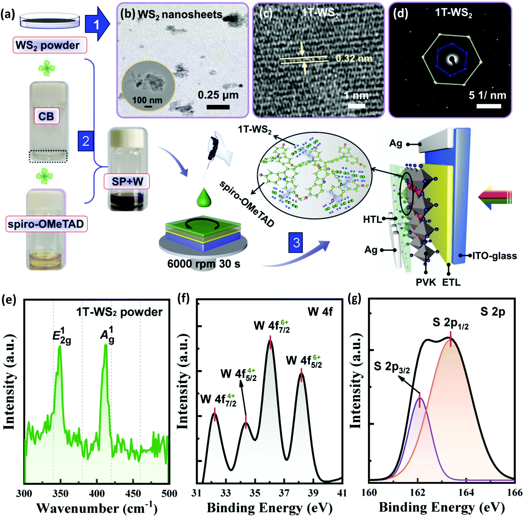 | ||
| Fig. 1 (a) Schematic of the manufacturing process of the SP + W hybrid HTL. Micrographs of commercial WS2 nanosheets: (b) TEM image, (c) HRTEM image, and (d) SAED pattern. (e) Raman spectrum of the WS2 nanosheets coated on the SiO2 substrate. Corresponding high-resolution XPS profiles: (f) W 4f and (g) S 2p. | ||
Transmission electron microscopy (TEM) was carried out to analyze the microstructure and morphology of the commercial WS2 nanosheets. Fig. 1(b) illustrates a typical TEM image of WS2 nanosheets with an average lateral size of approximately 100 nm. The homogeneous contrast of the nanosheets suggests that they consist of mono- and/or bilayers. To determine their crystalline structure, the samples were imaged using high-resolution transmission electron microscopy (HRTEM, Fig. 1(c)), revealing that the distorted 1T structure originated from the WS2 nanosheets (1T-WS2).27,28 This structure was generally observed when WS2 monolayers were prepared by Li exfoliation. The exfoliated WS2 sheets possessed a charged structure of [WS2]x−Lix+.28 Furthermore, the clear lattice fringes indicate the good crystallinity of the 1T-WS2 nanosheets. Fig. 1(d) shows the selected area electron diffraction (SAED) pattern, corresponding to the hexagonal crystal structure.28 The 1T-WS2 atomic model, presented in Fig. S1 (ESI†), exhibits a zigzag pattern, showing the locations of W and S atoms and their distorted 1T structural characteristics.27,28
Micro-Raman spectroscopy and X-ray photoelectron spectroscopy (XPS) were combined to further analyze and identify the material and chemical states of 1T-WS2. The Raman spectrum of the commercial WS2 nanosheets deposited on the SiO2 substrate is shown in Fig. 1(e). The spectrum displays two prominent first-order Raman-active modes, E12g and A1g, belonging to the 1T-phase of WS2.23,27,28 The corresponding peaks are located at approximately 348.9 and 412.3 cm−1, respectively. The E12g mode is associated with the in-plane vibration of W and S atoms, while the A1g mode is related to the out-of-plane vibration of S atoms.27,28 The distance between the peaks is approximately 63.4 cm−1, further evidencing that 1T-WS2 consists of mono- and/or bilayers—a finding supported by the literature.28 In addition, the high-resolution XPS spectrum of W 4f shown in Fig. 1(f) indicates that the two main peaks of W4f 7/2 and W4f 5/2 appear at 32.23 eV and 34.42 eV, respectively, representing the metallic 1T phase of WS2.24,27,28 Notably, the signals recorded at approximately 35.9 and 38.18 eV suggest the existence of W6+ species, probably due to the formation of W oxides (i.e., WO3) during exfoliation.24,28 Moreover, as shown in the high-resolution XPS spectrum of S 2p (Fig. 1(g)), the binding energies of the S 2p 3/2 and S 2p 1/2 peaks at 161.58 eV and 162.89 eV, respectively, can be attributed to the S2− in 1T-WS2.24,28 These results agree with those reported previously.22–24,26–28
Fig. 2(a) and (b) exhibit the cross-sectional scanning electron microscopy (SEM) images of the SP and SP + W HTLs. Since the addition of the 1T-WS2 dispersion lowered the concentration of the spiro-OMeTAD solution, the thickness of the hybrid HTL was significantly lower than that of a conventional HTL under the same deposition conditions (spin coating speed/time, drip amount, etc.). The specific processes of solution synthesis and film deposition are described in the Experimental section. The HRTEM image in Fig. 2(c) clearly demonstrates the presence and distribution of 1T-WS2 in the hybrid HTL. The microstructure of the film was characterized by directly coating the mixture onto the TEM grid.27 High crystallinity of the 1T-WS2 lattice domains was observed (see yellow regions), and an interplanar distance of approximately 0.32 nm was measured. These results are consistent with the observations in Fig. 1(c). No local accumulation or agglomeration was found, indicating that the nanosheets were uniformly dispersed in the hybrid HTL.29,30 The green region in Fig. 2(c) represents the typical amorphous spiro-OMeTAD, and the corresponding HRTEM image is given in Fig. S2 (ESI†). The Raman spectra and elemental mappings of W and S in Fig. S3 (ESI†) further confirm the existence and uniform distribution of 1T-WS2 in the hybrid HTL.
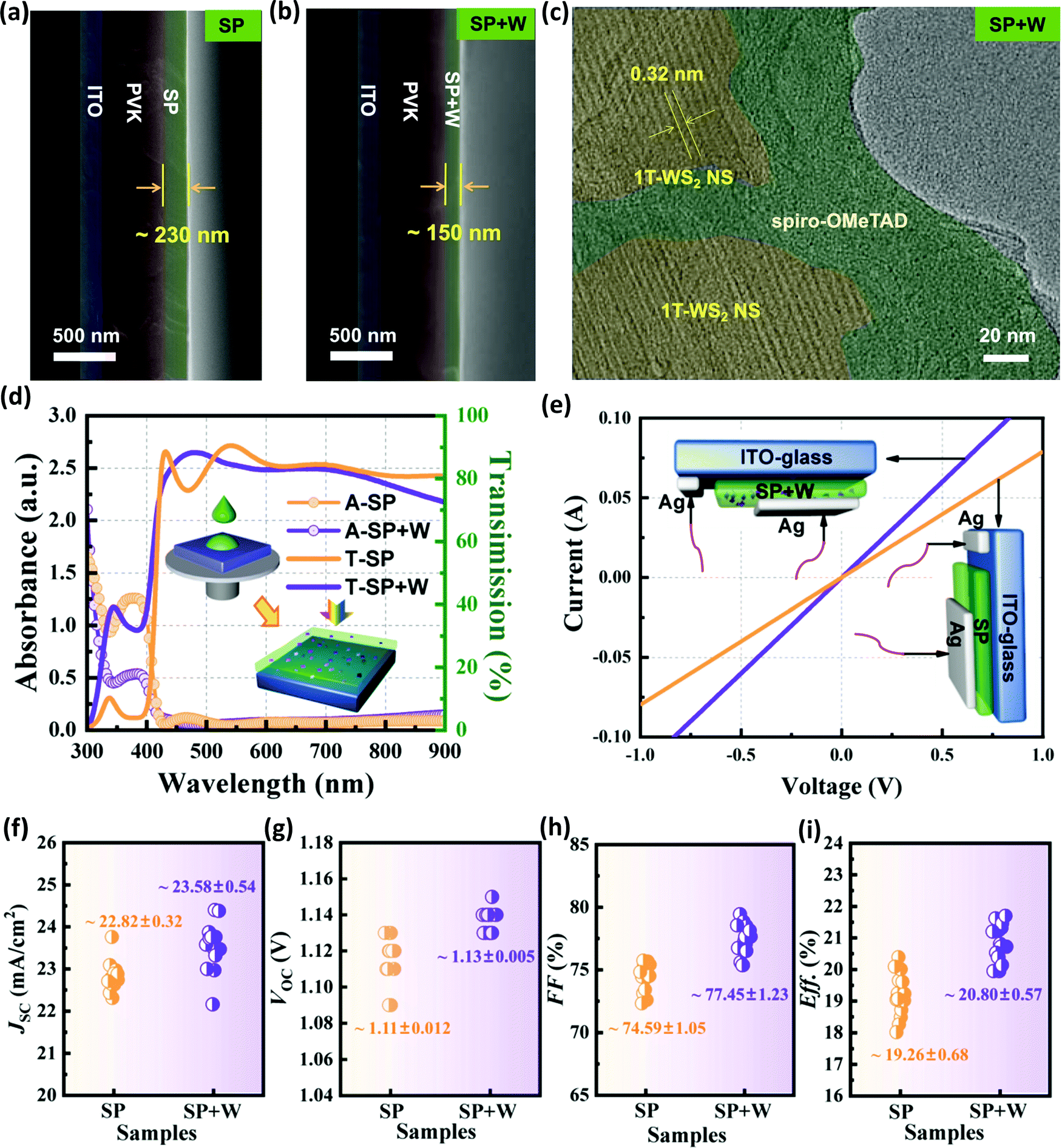 | ||
| Fig. 2 Cross-sectional SEM images of (a) ITO/PVK/SP and (b) ITO/PVK/SP + W samples. (c) HRTEM image of the SP + W hybrid HTL. (d) Optical properties of ITO/SP and ITO/SP + W substrates. (e) J–V characteristics of corresponding samples. Statistical analysis of the (f) JSC, (g) VOC, (h) FF, and (i) efficiency of 30 individual devices with different HTLs prepared under the same conditions. | ||
The decreased thickness of the hybrid HTL significantly improved its transmittance at a short wavelength (Fig. 2(d)), which is conducive to enhancing the backside light-harvesting capability and PV output of bifacial devices. The absorption spectra shown in Fig. 2(d) indicate that the conventional SP HTL has an absorption near 380 nm.12,13 Therefore, 1T-WS2-doped spiro-OMeTAD shows superior optical competitiveness in high-efficiency bifacial PV applications compared to the conventional SP HTL.
More importantly, the decrease in the thickness caused by 1T-WS2 does not lead to electrical losses in the hybrid HTL, but instead accelerates hole transfer in the improved system to a certain extent. The current–voltage (J–V) characteristics presented in Fig. 2(e) further verify the contribution of 1T-WS2 to the enhancement of the electrical properties of HTL. The charge dynamic enhancement of the SP + W film is attributed to the superior carrier mobility and metallic properties of 1T-WS2.21,22,24 Moreover, the planes of the W atoms in 1T-WS2 are sandwiched between two atomic layers of S with a strong in-plane bonding, and layers are stacked together via weak van der Waals interaction, showing metallic properties. Therefore, adding 1T-WS2 to the SP HTL is equivalent to p-doping of the hybrid film, resulting in improved hole mobility and film conductivity.21,24,25 Hall effect measurements of the corresponding samples further confirm the charge dynamic enhancement of the HTL induced by 1T-WS2. Table S1 (ESI†) shows the Hall measurement results of the two abovementioned HTLs. The conductivity and Hall mobility of the SP + W hybrid film are effectively improved compared with those of the SP film, and are not negatively affected by the film thickness loss. Moreover, the resistivity of the corresponding films also shows a similar tendency, indicating that 1T-WS2 promotes the electrical properties of the hybrid HTL.
The enhancement in the optical and electrical properties of the hybrid HTL caused by 1T-WS2 and the synergistic effect between them play an important role in improving the interface charge behavior, light collection ability, and PCE of b-PSCs. Consequently, the PV parameters of the PSCs using SP + W were generally superior to those of the SP-based PSCs, and the average PCE increased from approximately 19% to 21%. The statistical output parameters of 30 individual PSCs (15 cells based on SP + W, 15 cells based on SP) prepared by the same process are shown in Fig. 2(f)–(i), and a more detailed comparison of the PV parameters is also displayed.
In addition to the excellent photoelectric contribution of the SP + W hybrid HTL, the energy band and surface potential changes attributed to 1T-WS2 are also primarily responsible for improving the PV output of devices. The contact potential difference (CPD) of abovementioned two films was tested using Kelvin probe force microscopy (KPFM). The results summarized in Fig. 3(a) show that the average surface potential of the SP + W film is reduced to −140 mV—a value substantially lower than that of the control sample (approximately −90 mV). A lower surface potential implies that the hybrid HTL has a higher work function (WF) and a deeper Fermi level (Ef) compared to those of the SP HTL, resulting in a higher VOC for SP + W devices.31,32 To gain further insight into the mechanisms for the synergistic improvement in the energy band properties and PV parameters by 1T-WS2, ultraviolet photoelectron spectroscopy (UPS) was performed to verify the KPFM results.31,33 The band gaps (Eg) of the SP and SP + W films were extrapolated from the optical absorption spectra shown in Fig. S4 (ESI†). The corresponding Tauc plots presented in Fig. 3(b) show that their Eg values are almost similar. The UPS cut-off edge (Ecut-off) and Fermi edge (EF,edge) of the two samples are plotted in Fig. 3(c)–(f), respectively. After doping with 1T-WS2, the Ecut-off of the SP film was reduced from 16.76 to 16.60 eV, while EF,edge decreased from 0.76 to 0.69 eV. Therefore, the valence band (EVB) value of the SP + W film was estimated to be −5.31 eV, which is lower than that of the SP film (−5.22 eV). Additionally, the WF of the SP + W film was determined to be slightly higher than that of the SP film. The decrease in Ef caused by 1T-WS2 indicates that the EVB of the hybrid HTL is closer to that of the perovskite, effectively promoting hole extraction/transfer/collection, and ultimately increasing the VOC and FF of the device.34,35 Meanwhile, the improved level alignment is more conducive to reducing the interface energy barrier and suppressing the interface recombination and leakage current, thereby improving the PV performance of devices.34,35 The energy-level structures and possible charge behaviors are depicted in Fig. 3(g). In addition, the conduction band (ECB) values of the SP + W and SP films were calculated to be −2.29 and −2.22 eV, respectively, according to the relationship of ECB = EVB + Eg.31,35
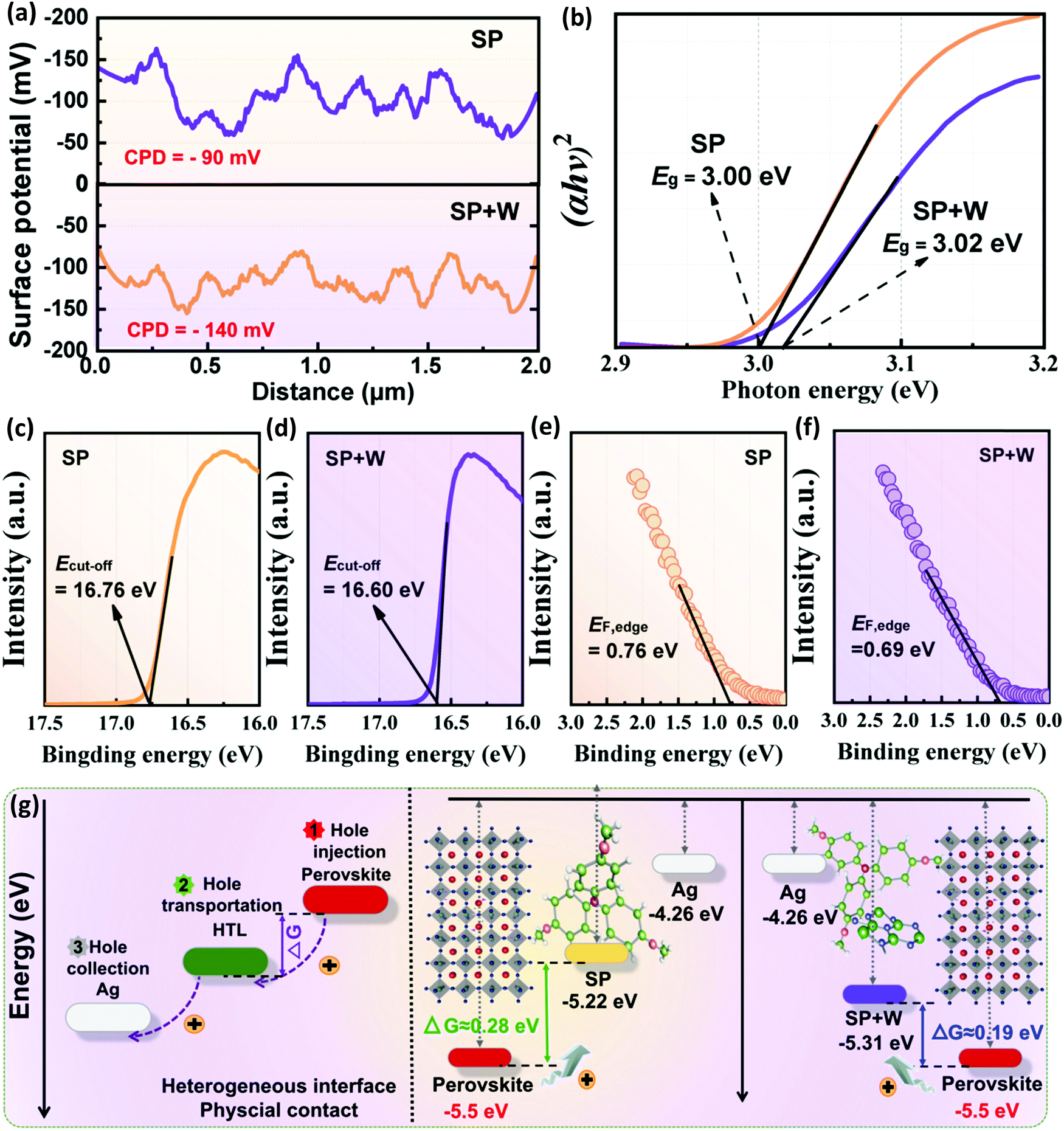 | ||
| Fig. 3 (a) KPFM images and (b) Tauc plots of SP and SP + W samples. (c and d) UPS cut-off edge (Ecut-off) and (e and f) Fermi edge (EF,edge) of the corresponding samples. (g) Schematic illustration of the carrier injection/transfer/collection processes based on the two abovementioned HTLs, according to band-gap alignments. | ||
Time-resolved photoluminescence (TRPL) and electrochemical impedance spectroscopy (EIS) measurements were employed to analyze the dynamic transport process of the hetero-interface carriers driven by IT-WS2. The TRPL curves were fitted using the bi-exponential decay function to obtain the lifetimes of the fast-decay and slow-decay carriers (τ1 and τ2, respectively; Fig. S5(a), ESI†). These terms correspond to the photoexcited charge carriers that are transported to the charge transport layer and undergo radiative decay, respectively.36,37 The τ1 and τ2 of the perovskite/SP + W sample were both shorter than those of the perovskite/SP sample, reflecting that IT-WS2 could promote carrier extraction/transfer/collection faster and more efficiently. The effects of different HTLs on the carrier extraction/recombination mechanisms in the PSCs were further analyzed using Nyquist plots measured at a bias voltage of 0.8 V in the dark. As shown in Fig. S5(b) (ESI†), the curves can be fitted using the equivalent fitted circuit model that includes a series resistance (Rs), charge transfer resistance (Rtr), recombination resistance (Rrec), and the correlated capacitance (C). In the EIS analysis, the Rs derived from Ohmic or electrical contacts stands for the sheet resistance of the transporting layers and charge-transfer resistance at the interface; The Rtr (fitted from the arc of the higher-frequency region) represents the heterointerface charge transfer and transportation resistance; The Rrec (derived from the arc fitting of the lower-frequency region) is the resistance of charges annihilated at the interface or within the perovskite lattice.33,34,36,38 The detailed parameters extracted from the fitting curves are summarized in Table S2 (ESI†). The Rtr and Rs values of the SP + W device are much smaller than those of the SP device, again confirming that IT-WS2 enhances the charge dynamics at the perovskite/HTL interface.36,38 Moreover, the SP + W device features a higher Rrec than that of the control SP device, reflecting a higher resistance for charge annihilation at the interface.36,38 These results, which are consistent with the UPS and TRPL observations, suggest that the reduction in the energy band barrier induced by IT-WS2 inhibits the heterointerface carrier aggregation and recombination, and effectively accelerates hole extraction/migration/collection, resulting in a significant improvement in the PV output of devices, especially short-circuit current density (JSC) and FF.36–39
The synergistic relationships among the hybrid HTL, charge behavior, and PV parameters of the solar cells were further elucidated by open-circuit photovoltage decay (OCVD) and dark-current measurements. The VOC decay curves shown in Fig. S6(a) (ESI†) indicate that the carrier recombination rate of the SP + W device is slower than that of the SP device under open-circuit conditions, demonstrating that the hybrid HTL improved the electrical properties and VOC of devices.40,41 The asymmetric dark J–V current response reveals the leakage current formed by carrier recombination in solar cells.40,41 As seen in Fig. S6(b) (ESI†), the hybrid HTL prevents the current leakage caused by charge recombination to a certain extent, and guarantees efficient PV output of solar cells, with notable improvements in JSC and FF.
Owing to the positive contributions of the hybrid HTL, it was used as the RWL in b-PSCs to achieve a synchronous improvement in the bidirectional PCEs. The ideal photoelectric balance in the hybrid RWL was obtained by regulating the volume ratio of the spiro-OMeTAD and 1T-WS2 solutions. The transmittance, absorption, and conductivity of the SP + W films with different volume ratios are shown in Fig. S7(a)–(c) (ESI†). A comparison of the results for the optimization of the RWL for efficient b-PSCs revealed that the sample with an SP:W ratio of 3:2 was suitable for subsequent studies.
The J–V test model of the b-PSC prepared in this work is depicted in Fig. 4(a). A shadow mask, set at 0.2 cm2 for front illumination and 0.12 cm2 for rear illumination, was used to define the active area of the bifacial device during J–V testing. Fig. 4(b) and (c) present the J–V curves, external quantum efficiency (EQE), and integrated JSC of the optimized SP + W b-PSC illuminated on different sides. The detailed J–V parameters are summarized in the inset of Fig. 4(b). The maximum efficiencies under front and rear illuminations were, respectively, 19.87% and 15.48%, which were higher than the PV output of the optimized SP b-PSC (Fig. S8(a), ESI,† optimized J–V curves of the SP b-PSC). Furthermore, the EQE spectra (Fig. 4(c)) show the peak spectral responses of the SP + W device under front and rear illuminations, especially its rear integrated JSC, are higher than those of the SP device (as shown in Fig. S8(b), ESI†).
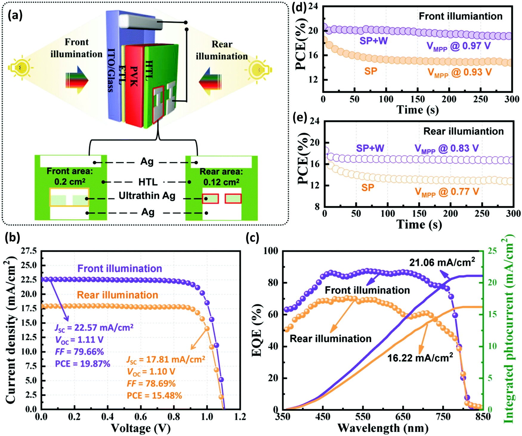 | ||
| Fig. 4 (a) Structure and PV test model of the b-PSC. (b) J–V characteristics and (c) corresponding EQE spectra of the best-performing SP + W b-PSC illuminated on different sides. (d) and (e) Steady-state PCEs measured at the voltage of the maximum power point for the two b-PSCs. | ||
Fig. S9 (ESI†) and Fig. 4(d) and (e) indicate the steady-state photocurrent and steady-state efficiencies measured at the voltage of the maximum power point (Vmpp) for the two b-PSCs. As expected, the SP + W device exhibited more stabilized current densities and efficiencies than the one without 1T-WS2 under one-sun illumination for 300 s, reflecting ideal irradiation stability. The stabilized current densities of the SP + W device were 21.00 mA cm−2 and 16.58 mA cm−2 under front and rear illuminations, respectively, and the corresponding efficiencies were 19.21 and 17.00%, respectively. For the SP b-PSC, the current densities were stabilized at 17.00 mA cm−2 and 11.65 mA cm−2 under front and rear illuminations, respectively, and the corresponding efficiencies were 15.02% and 13.11%, respectively. Accordingly, the improved PV output was attributed to synchronous improvements in the light-harvesting capability, energy-level alignment, and charge dynamics of the b-PSCs driven by 1T-WS2.
The hybrid RWL created in this work can also effectively alleviate the PV degradation caused by water erosion and photo-thermal degradation of solar cells during environmental testing. Unencapsulated SP and SP + W devices were stored in a controlled environment with the humidity and temperature set at 55 ± 5% and 40 ± 5 °C, respectively. The operational stability was then tracked under AM 1.5G of continuous irradiation. The controlled environment for observing the stability of b-PSCs is shown in Fig. 5(a), while the PV performance changes are presented in Fig. 5(e) and (f). After continuous illumination for 150 min, the SP + W device exhibited an improved PV stability, where the front PCE maintained approximately 84% of its initial value and rear PCE, approximately 70%. On the other hand, the front and rear efficiencies of the SP device decreased by approximately 50%. The PV attenuation of the SP-based b-PSC is due to the deliquescence and instability of the traditional SP HTL, which accelerates the degradation of perovskite.12–14 In contrast, the SP + W b-PSC has a relatively low spiro-OMeTAD content; further, the intrinsic thermal, chemical, and photochemical stabilities of 1T-WS2 mitigate device degradation upon illumination, at elevated temperatures, and during possible interactions with the organic/perovskite layer.23,25,31 Hence, the operational stability of the bifacial device is significantly improved.
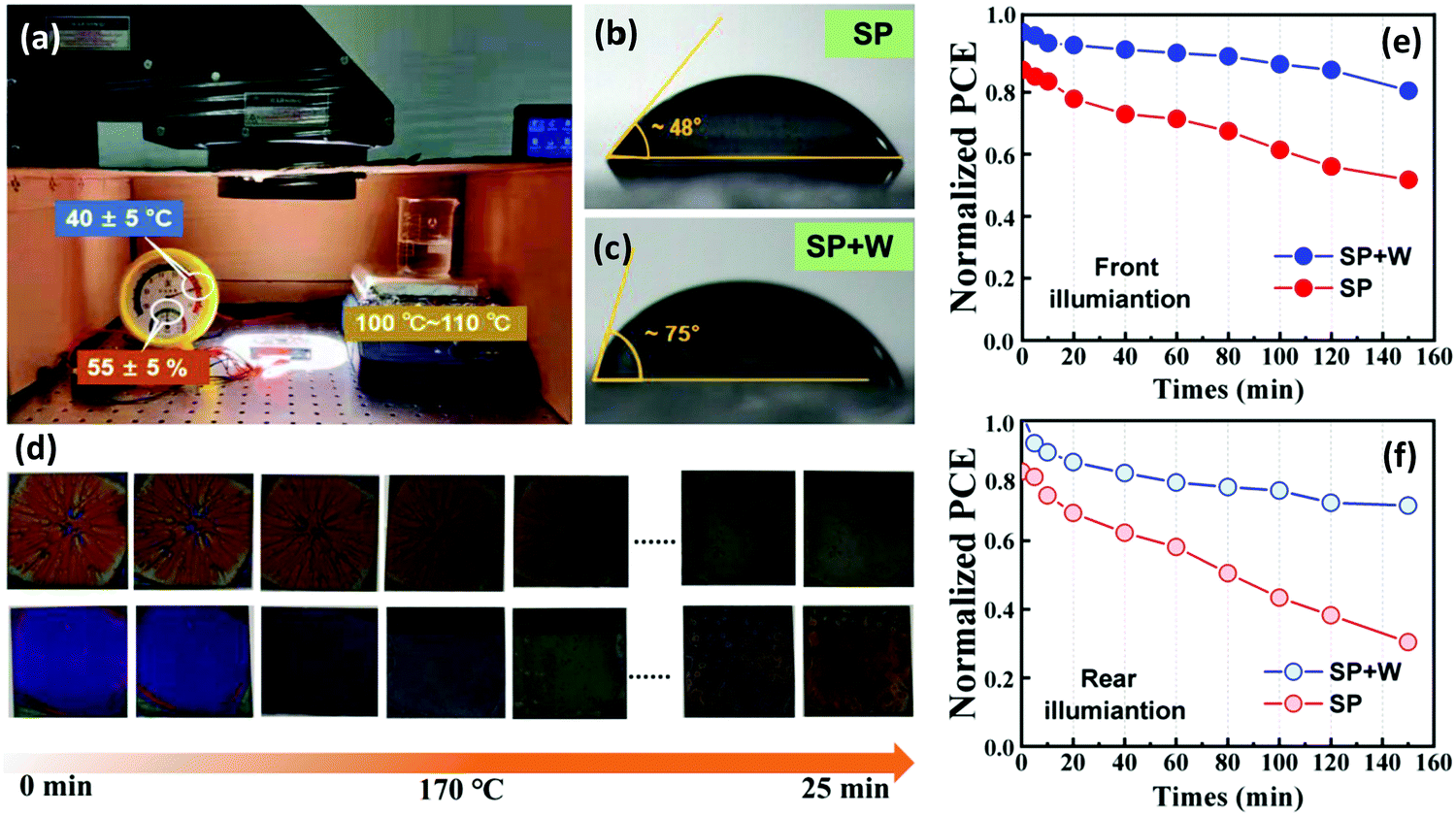 | ||
| Fig. 5 (a) Setup used to examine the operational stability of b-PSCs in a controlled environment. A beaker with deionized water was used to create a high-humidity environment, and the hygrometer in the chamber was used to monitor the closed environment. Water contact angles of (b) SP and (c) SP + W films. (d) Morphological and microstructure changes in the corresponding films as a function of the testing time in a high-temperature environment. (e and f) PV output stability tests of the unencapsulated devices based on different HTLs under continuous front and rear illuminations (100 mW cm−2). | ||
Fig. 5(b) and (c) indicate that the water contact angle (WCA ≈ 75°) of the SP + W film is significantly larger than that of the SP film (WCA ≈ 48°), confirming superior hydrophobicity and stability of the hybrid RWL. In addition, the hybrid RWL offers a higher heat resistance than the traditional organic RWL. From Fig. 5(d), the PVK/SP + W sample degrades at a lower rate than the PVK/SP sample under the operating conditions or a thermal environment, which is attributed to 1T-WS2 suppressing the movement of some active ions in the hybrid system (e.g., the migration/diffusion of Li ions in spiro-OMeTAD, the precipitation/migration of inorganic/organic ions in the absorber).39,41–44 The comprehensive results show that 1T-WS2 plays an important role in improving the PV output and stability of b-PSCs. Such findings can drive the rapid development of innovative PV devices in the industry.
4. Conclusions and perspectives
A novel strategy to improve the photoelectric balance of RWLs for efficient b-PSCs was developed by constructing an organic–inorganic hybrid SP + W HTL using a simple spin-coating method. By optimizing the physical and photoelectric properties of the hybrid system, the mechanisms responsible for the synergistic effects on the light-harvesting capability, charge dynamics, and PV output parameters of bifacial devices were determined. The optimized device exhibited maximum efficiencies of 19.87% and 15.48% under front and rear illuminations, respectively. The enhanced PV characteristics were attributed to simultaneous improvements in the optical transmittance and internal hole transfer of the hybrid HTL by 1T-WS2 doping. Furthermore, the surface potential reduction, energy-level alignment, and photo-generated charge extraction/migration/collection acceleration of the hybrid HTL caused by 1T-WS2, as well as their synergistic effects, make an important contribution to improving the bidirectional PV outputs of the device and reducing recombination losses. Notably, the unencapsulated hybrid b-PSC exhibited better irradiation/operation stability than the control SP-based b-PSC. This is due to the intrinsic thermal, chemical, and photochemical stabilities of 1T-WS2 in the hybrid HTL, which alleviated the PV degradation of the device in illumination and in thermal environments. This work therefore provides important insights into materials selection, structural design, and performance optimization for the development of high-quality RWLs. It also establishes a promising new platform for more efficient and stable b-PSCs and other PV devices, such as flexible, and tandem solar cells.Author contributions
Lin Fan, Jinghai Yang, and Lili Yang designed the devices and supervised the progress of this project. Wanhong Lü and Wanting Hu synthesized the materials and fabricated the solar cells. Donglai Han, Shuo Yang, Dandan Wang, and Zhihong Mai carried out material characterization and electrical measurements. Fengyou Wang and Huilian Liu helped in the discussion of materials and device characterization. Lin Fan wrote the manuscript, and all authors revised the paper.Conflicts of interest
The authors declare no competing financial interest.Acknowledgements
The authors gratefully acknowledge the support from the National Natural Science Foundation of China (Grant No. 61904066, 22075101, 11904127, and 11904129), the Program for the Development of Science and Technology of Jilin Province (Item No. 20210509050RQ, 20200801032GH, 20210101410JC, 20200201022JC, and 20200301043RQ), the Program for the Science and Technology of Education Department of Jilin Province (Item No. JJKH20210440KJ, JJKH20210611KJ, JJKH20220442KJ, and JJKH20210447KJ), and the Program of Jilin Provincial Development and Reform Commission (Grant No. 2021C036-3).References
- Y. Zhao, T. Heumueller, J. Zhang, J. Luo, O. Kasian, S. Langner, C. Kupfer, B. Liu, Y. Zhong, J. Elia, A. Osvet, J. Wu, C. Liu, Z. Wan, C. Jia, N. Li, J. Hauch and C. J. Brabec, A bilayer conducting polymer structure for planar perovskite solar cells with over 1,400hours operational stability at elevated temperatures, Nat. Energy, 2021, 7, 144–152 CrossRef.
- Y. Hou, E. Aydin, M. D. Bastiani, C. Xiao, F. H. Isikgor, D. J. Xue, B. Chen, H. Chen, B. Bahrami, A. H. Chowdhury, A. Johnston, S. W. Baek, Z. Huang, M. Wei, Y. Dong, J. Troughton, R. Jalmood, A. J. Mirabelli, T. G. Allen, E. V. Kerschaver, M. I. Saidaminov, D. Baran, Q. Qiao, K. Zhu, S. D. Wolf and E. H. Sargent, Efficient tandem solar cells with solution-processed perovskite on textured crystalline silicon, Science, 2020, 367, 1135–1140 CrossRef CAS PubMed.
- A. Kotta, I. Seo, H. S. Shin and H. K. Seo, Room-temperature processed hole-transport layer in flexible inverted perovskite solar cell module, Chem. Eng. J., 2022, 435, 134805 CrossRef CAS.
- C. Hanmandlu, C. Y. Chen, K. M. Boopathi, H. W. Lin, C. S. Lai and C. W. Chu, Bifacial perovskite solar cells featuring semitransparent electrodes, ACS Appl. Mater. Interfaces, 2017, 9, 32635–32642 CrossRef CAS PubMed.
- F. Liang, Z. Ying, Y. Lin, B. Tu, Z. Zhang, Y. Zhu, H. Pan, H. Li, L. Luo, O. Ageev and Z. He, High-performance semitransparent and bifacial perovskite solar cells with MoOx/Ag/WOx as the rear transparent electrode, Adv. Mater. Interfaces, 2020, 7, 2000591 CrossRef CAS.
- K. K. Sonigara, Z. Shao, J. Prasad, H. K. Machhi, G. Cui, S. Pang and S. S. Soni, Organic ionic plastic crystals as hole transporting layer for stable and efficient perovskite solar cells, Adv. Funct. Mater., 2020, 30, 2001460 CrossRef CAS.
- Z. Song, C. Chen, C. Li, S. Rijal, L. Chen, Y. Li and Y. Yan, Assessing the true power of bifacial perovskite solar cells under concurrent bifacial illumination, Sustainable Energy Fuels, 2021, 5, 2865–2870 RSC.
- A. Al-ashouri, E. Khnen, B. Li, A. Magomedov and S. Albrecht, Monolithic perovskite/silicon tandem solar cell with >29% efficiency by enhanced hole extraction, Science, 2020, 370, 1300–1309 CrossRef CAS PubMed.
- National Renewable Energy Laboratory Best Research-Cell Effciency, Chart, https://www.nrel.gov/pv/cell-efficiency.html.
- W. Lü, L. Fan, M. Wang, P. Wang, Q. Sun, S. Yang, D. Han, F. Wang, H. Liu, J. Yang and L. Yang, Photoelectric balance of rear electrode in bifacial perovskite solar cells: Construction of 0D/1D/2D composite electrode based on silver nanowires to boost photovoltaic output, J. Power Sources, 2022, 520, 230815 CrossRef.
- L. Fan, Y. Li, X. Yao, Y. Ding, S. Zhao, B. Shi, C. Wei, D. Zhang, B. Li, G. Wang, Y. Zhao and X. Zhang, Delayed annealing treatment for high-quality CuSCN: Exploring its impact on bifacial semitransparent n-i-p planar perovskite solar cells, ACS Appl. Energy Mater., 2018, 1, 1575–1584 CrossRef CAS.
- M. Elawad, K. I. John, A. M. Idris, L. Yang and Y. Gao, An organic hole-transporting material spiro-OMeTAD doped with a Mn complex for efficient perovskite solar cells with high conversion efficiency, RSC Adv., 2021, 11, 32730–32739 RSC.
- A. Pellaroque, N. K. Noel, S. N. Habisreutinger, Y. Zhang, S. Barlow, S. R. Marder and H. J. Snaith, Efficient and stable perovskite solar cells using molybdenum tris(dithiolene)s as p-dopants for spiro-OMeTAD, ACS Energy Lett., 2017, 2, 2044–2050 CrossRef CAS.
- V. E. Madhavan, I. Zimmermann, A. A. B. Baloch, A. Manekkathodi, A. Belaidi, N. Tabet and M. K. Nazeeruddin, CuSCN as hole transport material with 3D/2D perovskite solar cells, ACS Appl. Energy Mater., 2019, 3, 114–121 CrossRef.
- M. Liang, A. Ali, A. Belaidi, M. I. Hossain, O. Ronan, C. Downing, N. Tabet, S. Sanvito, F. Ei-Mellouhi and V. Nicolosi, Improving stability of organometallic-halide perovskite solar cells using exfoliation two-dimensional molybdenum chalcogenides, npj 2D Mater. Appl., 2020, 4, 40 CrossRef CAS.
- X. Liu, H. W. Qiao, M. Chen, B. Ge, S. Yang, Y. Hou and H. G. Yang, Inverted perovskite solar cells based on potassium salt-modified NiOX hole transport layers, Mater. Chem. Front., 2021, 5, 3614 RSC.
- Y. Jiang, S. Chen, W. Zheng, B. Zheng and A. Pan, Interlayer exciton formation, relaxation, and transport in TMD van der Waals heterostructures, Light: Sci. Appl., 2021, 10, 72 CrossRef CAS PubMed.
- Y. Lin, B. Adilbekova, Y. Firdaus, E. Yengel, H. Faber, M. Sajjad, X. Zheng, E. Yarali, A. Seitkhan, O. M. Bakr, A. El-Labban, U. Schwingenschlögl, V. Tung, I. McCulloch, F. Laquai and T. D. Anthopoulos, 17% efficient organic solar cells based on liquid exfoliated WS2 as a replacement for PEDOT:PSS, Adv. Mater., 2019, 31, 1902965 CrossRef CAS PubMed.
- E. Singh, K. S. Kim, G. Y. Yeom and H. S. Nalwa, Atomically thin-layered molybdenum disulfide (MoS2) for bulk heterojunction solar cells, ACS Appl. Mater. Interfaces, 2017, 94, 3223 CrossRef PubMed.
- Q. Zhou, J. Duan, X. Yang, Y. Duan and Q. Tang, Interfacial strain release from the WS2/CsPbBr3 van der Waals heterostructure for 1.7 V voltage all-inorganic perovskite solar cells, Angew. Chem., Int. Ed., 2020, 59, 21997–22001 CrossRef CAS PubMed.
- Q. Cao, Y. W. Dai, J. Xu, L. Chen, H. Zhu, Q. Q. Sun and D. W. Zhang, Realizing stable p-type transporting in two-dimensional WS2 films, ACS Appl. Mater. Interfaces, 2017, 9, 18215–18221 CrossRef CAS PubMed.
- Y. G. Kim, K. C. Kwon, Q. V. Le, K. Hong, H. W. Jang and S. Y. Kim, Atomically thin two-dimensional materials as hole extraction layers in organolead halide perovskite photovoltaic cells, J. Power Sources, 2016, 319, 1–8 CrossRef CAS.
- P. Huang, Z. Wang, Y. Liu, K. Zhang, L. Yuan, Y. Zhou, B. Song and Y. Li, Water-soluble 2D transition metal dichalcogenides as the hole-transport layer for highly efficient and stable p-i-n perovskite solar cells, ACS Appl. Mater. Interfaces, 2017, 9, 25323–25331 CrossRef CAS PubMed.
- H. N. Hemasiri, S. Kazim and S. Ahmad, 1T-Rich 2D-WS2 as an interfacial agent to escalate photo-induced charge transfer dynamics in dopant-free perovskite solar cells, J. Mater. Chem. C, 2021, 9, 9865–9873 RSC.
- L. L. Jiang, Z. K. Wang, M. Li, C. H. Li, P. F. Fang and L. S. Liao, Flower-like MoS2 nanocrystals: a powerful sorbent of Li+ in the spiro-OMeTAD layer for highly efficient and stable perovskite solar cells, J. Mater. Chem. A, 2019, 7, 3655–3663 RSC.
- J. Cao, G. Tang, P. You, T. Wang, F. Zheng, J. Zhao and F. Yan, Enhanced performance of planar perovskite solar cells induced by van der Waals epitaxial growth of mixed perovskite films on WS2 Flakes, Adv. Funct. Mater., 2020, 30, 2002358 CrossRef CAS.
- X. Tong, Y. Qi, J. Chen, N. Wang and Q. Xu, Supercritical CO2-assisted reverse-micelle-induced solution-phase fabrication of two-dimensional metallic 1T-MoS2 and 1T-WS2, ChemNanoMat, 2017, 3, 466–471 CrossRef CAS.
- B. Mahler, V. Hoepfner, K. Liao and G. A. Ozin, Colloidal synthesis of 1T-WS2 and 2H-WS2 nanosheets: applications for photocatalytic hydrogen evolution, J. Am. Chem. Soc., 2014, 136, 14121–14127 CrossRef CAS PubMed.
- P. Qiu, J. Wang, Z. Liang, Y. Xue, Y. Zhou, X. Zhang, H. Cui, G. Cheng and J. Tian, The metallic 1T-WS2 as cocatalysts for promoting photocatalytic N2 fixation performance of Bi5O7Br nanosheets, Chin. Chem. Lett., 2021, 32, 3501–3504 CrossRef CAS.
- W. Zhao, Z. Ghorannevis, K. K. Amara, J. R. Pang, M. Toh, X. Zhang, C. Kloc, P. H. Tan and G. Eda, Lattice dynamics in mono-and few-layer sheets of WS2 and WSe2, Nanoscale, 2013, 5, 9677–9683 RSC.
- X. Wang, J. Wu, Y. Yang, G. Li, Z. Song, X. Liu, W. Sun, Z. Lan and P. Gao, Chromium trioxide modified spiro-OMeTAD for highly efficient and stable planar perovskite solar cells, J. Energy Chem., 2021, 61, 386–394 CrossRef.
- D. Li, Y. Huang, G. Wang, Q. Lian, R. Shi, L. Zhang, X. Wang, F. Gao, W. Kong, B. Xu, C. Cheng and S. Li, Boosting the performance of MA-free inverted perovskite solar cells via multifunctional ion liquid, J. Mater. Chem. A, 2021, 9, 12746–12754 RSC.
- L. Fan, P. Wang, M. Wang, W. Lü, F. Wang, H. Liu, J. Yang and L. Yang, Exploring low-temperature processed multifunctional HEPES-Au NSs-modified SnO2 for efficient planar perovskite solar cells, Chem. Eng. J., 2022, 427, 131832 CrossRef CAS.
- F. Wang, M. Yang, Y. Zhang, J. Du, S. Yang, L. Yang, L. Fan, Y. Sui, Y. Sun and J. Yang, Full-scale chemical and field-effect passivation: 21.52% efficiency of stable MAPbI3 solar cells via benzenamine modification, Nano Res., 2021, 14, 2783–2789 CrossRef CAS.
- L. Fan, Y. Ding, B. Shi, C. Wei, D. Zhang, J. Xie, X. Yu, B. Yan, Y. Zhao and X. Zhang, Novel insight into the function of PC61BM in efficient planar perovskite solar cells, Nano Energy, 2016, 27, 561–568 CrossRef CAS.
- M. Wang, L. Fan, W. Lv, Q. Sun, X. Wang, F. Wang, J. Yang, H. Liu and L. Yang, Interior/interface modification of textured perovskite for enhanced photovoltaic outputs of planar solar cells by an in situ growth passivation technology, ACS Appl. Mater. Interfaces, 2021, 13, 39689–39700 CrossRef CAS PubMed.
- S. Wang, Y. Hua, M. Wang, F. Liu and L. Ding, CsPbI2.69Br0.31 solar cells from low-temperature fabrication, Mater. Chem. Front., 2019, 3, 1139–1142 RSC.
- L. Fan, P. Wang, S. Yang, L. Yang, F. Wang, X. Liu, M. Wei, H. Liu, Y. Sui and F. Rosei, Constructing “hillocks”-like random-textured absorber for efficient planar perovskite solar cells, Chem. Eng. J., 2020, 387, 124091 CrossRef CAS.
- J. Y. Du, Y. H. Zhang, M. F. Yang, D. L. Han, L. Fan, Y. R. Sui, J. Yang, L. L. Yang and F. Y. Wang, Hot-carrier injection antennas with hemispherical AgOx@Ag architecture for boosting the efficiency of perovskite solar cells, ACS Appl. Mater. Interfaces, 2020, 12, 41446–41453 CrossRef CAS PubMed.
- X. Li, J. Du, H. Duan, H. Wang, L. Fan, Y. Sun, Y. Sui, J. Yang, F. Wang and L. Yang, Moisture-preventing MAPbI3 solar cells with high photovoltaic performance via multiple ligand engineering, Nano Res., 2022, 15, 1375–1382 CrossRef CAS.
- Y. S. Sun, Z. Y. Pang, Y. N. Quan, D. L. Han, X. Y. Zhang, X. Ge, F. Y. Wang, Y. F. Sun, J. H. Yang and L. L. Yang, A synchronous defect passivation strategy for constructing high-performance and stable planar perovskite solar cells, Chem. Eng. J., 2020, 413, 127387 CrossRef.
- L. Fan, Y. Ding, J. S. Luo, B. Shi, X. Yao, C. C. Wei, D. K. Zhang, G. C. Wang, Y. Sheng, Y. F. Chen, A. Hagfeldt, Y. Zhao and X. D. Zhang, Elucidating the role of chlorine in perovskite solar cells, J. Mater. Chem. A, 2017, 5, 7423–7432 RSC.
- Y. Ou, A. Sun, H. Li, T. Wu, D. Zhang and P. Xu, Developing D-π-D hole-transport materials for perovskite solar cells: the effect of the p-bridge on device performance, Mater. Chem. Front., 2021, 5, 876–884 RSC.
- Y. Yuan, J. Chae, Y. Shao, Q. Wang, Z. Xiao, A. Centrone and J. Huang, Photovoltaic switching mechanism in lateral structure hybrid perovskite solar cells, Adv. Energy Mater., 2015, 5, 1500615 CrossRef.
Footnote |
| † Electronic supplementary information (ESI) available. See DOI: https://doi.org/10.1039/d2qm00366j |
| This journal is © the Partner Organisations 2022 |