
Achieving a near-unity photoluminescence quantum yield and high stability of CsPbI3 nanoplatelets by hydroiodic acid-assisted ligand treatment†
Zongnan
Li‡
,
Yusheng
Song‡
,
Sheng
Cao
 *,
Ke
Xing
,
Zhentao
Du
,
Bingsuo
Zou
and
Jialong
Zhao
*
*,
Ke
Xing
,
Zhentao
Du
,
Bingsuo
Zou
and
Jialong
Zhao
*
School of Physical Science and Technology, State Key Laboratory of Featured Metal Materials and Life-cycle Safety for Composite Structures, Guangxi University, Nanning 530004, China. E-mail: caosheng@gxu.edu.cn; zhaojl@gxu.edu.cn
First published on 10th March 2024
Abstract
Perovskite nanoplatelets (NPLs) display excellent photoluminescence (PL) properties and unique shape features, including thickness-dependent bandgap luminescence. However, perovskite NPLs, especially those based on iodides, exhibit poor spectral and phase stability. Herein, we propose a facile strategy to achieve a near-unity PL quantum yield (QY) and high stability of CsPbI3 NPLs by employing hydrogen iodate (HI) for in situ etching-assisted surface modification of the short-chain strongly bound ligand dodecylamine (DDDAm). It is found that HI can etch off the incomplete octahedron [PbI6]4− on the surface of CsPbI3 NPLs. Simultaneously, the excessive use of I− ions and the introduction of DDDAm ligands effectively passivate the surface defects of NPLs, significantly improving their radiation recombination rate. As a result, the as-prepared CsPbI3 NPLs exhibit up to 95% PL QY, maintaining PL characteristics even after 87 days of exposure to the atmospheric environment. Conversely, untreated CsPbI3 NPLs display poor phase stability and transform into non-PL features (δ-CsPbI3) after 21 days. As a proof of concept, we fabricated perovskite LEDs (PeLEDs) using these treated CsPbI3 NPLs as luminescent layers for calibration. These PeLEDs showcase bright electroluminescence at 600 nm, with a full width at half maximum of 22 nm and an external quantum efficiency of 2.98%. The effective synthesis strategy using HI-assisted ligand treatment presented here is expected to be extended to the synthesis of other perovskite NPLs, thereby accelerating the integration of perovskite NPLs in optoelectronic technology.
1. Introduction
All-inorganic perovskites have emerged as excellent candidates for light emitting diodes (LEDs), photodetectors, solar cells, and lasers because of their adjustable emitting range, high photoluminescence quantum yields (PL QYs), and high color purity.1–7 Among these, perovskite nanoplatelets (NPLs) with varying thicknesses exhibit distinctive properties in bandgap tuning and photophysics, serving as valuable complements to perovskite quantum dots (QDs) and other nanoscale perovskites.8–10 The controlled thickness of perovskite NPLs allows them to effectively address issues associated with other tuning methods, such as phase separation in mixed halide methods or severe aggregation in ultra-small QDs.11,12 Consequently, these unique optoelectronic properties position perovskite NPLs as highly anticipated emerging materials in the optoelectronic field.Despite the considerable potential of perovskite NPLs, their development significantly lags behind that of perovskite QDs, primarily due to inadequate stability.13–15 During sample storage or film preparation, perovskite NPLs may undergo face-to-face or side-by-side fusion, resulting in changes in the emission color and even phase transitions.16,17 For instance, face-to-face fusion can transform NPLs into bulks, diminishing quantum confinement effects and causing a redshift in emission.18–20 This undesirable redshift poses a challenge for preparing red and blue emitters based on pure iodide and pure bromide perovskite NPLs, as achieving the required emission wavelength necessitates a quantum confinement-induced blueshift.21–23 In addition to changes in the emission color, phase transitions in iodide-based NPLs present another challenge.24–26 α-CsPbI3 is inherently unstable due to its cubic nature; Cs+ ions in CsPbI3 are insufficient to stabilize the cubic framework of the [PbI6]4− octahedron, allowing for phase transitions through dynamic motion.27–30 Specifically, due to the low thickness and small width of CsPbI3 NPLs, the area of the two planes is minimal, resulting in almost no ligand encapsulation.31–33 Consequently, these CsPbI3 NPLs tend to form nanowires through side-by-side fusion, typically found in δ-CsPbI3 non-perovskite regions.34–37 Current efforts to suppress perovskite QD fusion primarily focus on surface chemical improvements, including passivation of halogen defects or connecting strong ligands.38,39 However, the reported surface treatment methods of perovskite QDs still face significant challenges in achieving both high stability and high luminescence performance for perovskite NPLs due to their inherently large specific surface area.40–42
In the present work, for the first time, we report a hydroiodic acid (HI)-assisted ligand treatment method to obtain a near-unity quantum yield and excellent stability of CsPbI3 NPLs. The incorporation of HI and the strong partial L-type coordination of the dodecylamine (DDDAm) ligand into CsPbI3 NPLs were systematically studied to assess their impact on stability and luminescence properties. The results reveal that the introduced HI effectively etches the incomplete octahedron [PbI6]4− on the surface of CsPbI3 NPLs, leading to a shift of the emission peak from 635 nm to 600 nm, indicating a more pronounced quantum confinement effect. The surface defects of CsPbI3 NPLs are efficiently passivated with excess I− ions and the newly introduced DDDAm ligands, significantly improving the radiative recombination rate. The photoluminescence QY of CsPbI3 NPLs optimized by HI and new short-chain ligands can reach up to 95%, and their PL properties can be maintained even after 87 days of exposure to the atmospheric environment. In contrast, untreated modified CsPbI3 NPLs exhibit poor phase stability, transforming into the non-optical phase of δ-CsPbI3 after 21 days. Additionally, we explored the potential application of these CsPbI3 NPLs in perovskite LEDs (PeLEDs). Utilizing the spin-coating solution processing technology, we successfully prepared PeLEDs based on these treated NPLs, showcasing bright electroluminescence (EL) at 600 nm, with a full width at half maximum (FWHM) of 22 nm and an external quantum efficiency (EQE) of 2.98%. This HI-assisted ligand treatment method presents a feasible strategy for preparing highly stable and low-defect CsPbI3 NPLs, and it is anticipated that this method can be extended to the synthesis of other perovskite NPLs, contributing to the accelerated application of perovskite NPLs in optoelectronic technology.
2. Results and discussion
The CsPbI3 NPLs were synthesized using a dynamic control method by varying the synthesis temperature. As observed in previous studies,43,44 the PL peak of CsPbI3 NPLs gradually shifts towards the blue side as the reaction temperature decreases, attributed to the enhanced quantum confinement effect (Fig. S1, ESI†). Simultaneously, the PL QY of CsPbI3 NPLs with a strong confinement effect decreases gradually with the blue shift of the emission peak (Fig. S2, ESI†). At a PL wavelength of 635 nm, the PL QY of CsPbI3 NPLs is only 12%, primarily due to the limitations imposed by a larger specific surface area on small-sized NPLs, making them more susceptible to non-radiative transitions caused by surface defects. In an attempt to mitigate the impact of surface defects on PL QY, a widely-used strong local L-shaped ligand, DDDAm, was employed for synergistic coordination modification of the NPLs. Introduction of DDDAm increased the PL QY of CsPbI3 NPLs from 12% to 51% (Fig. S3, ESI†). However, due to the larger specific surface area of CsPbI3 NPLs compared to QDs, this classical ligand modification method in QD systems has not been able to achieve the ideal near-unity PL QY for CsPbI3 NPLs.To address surface defects caused by the high specific surface area, we propose a strategy that combines acid etching and ligand exchange to prepare high-quality CsPbI3 NPLs. As illustrated in Fig. 1a, HI was introduced into the synthesis process of CsPbI3 NPLs to etch the incomplete octahedral [PbI6]4− on the surface of the NPLs, creating a halogen-rich environment on its surface to passivate halogen defects. Fig. 1b and c demonstrate that the PL peak of CsPbI3 NPLs shifted from 635 nm to 600 nm after etching, and the corresponding PL QY increased from 12% to 47.8%. It is noteworthy that the amount of HI added significantly modulates the PL performance of CsPbI3 NPLs (Fig. S4 and 5, ESI†). This is because the addition of HI not only etches the incomplete octahedral [PbI6]4− on the surface of CsPbI3 NPLs, but also removes the weakly bound long-chain ligands oleic acid (OA) and oleamine (OAm), exposing more vacancy defects. After introducing the short-branched strong L-shaped ligand, DDDAm replaced the easily detachable OA/OAm and further passivated the surface defects of NPLs. As depicted in Fig. 1d, the PL peak of the treated CsPbI3 NPLs remains at 600 nm, and the highest PL QY can reach 95% with good repeatability (Fig. S6, ESI†). The absorption spectra showed that the etched NPLs and treated NPLs possessed higher valley/peak ratios compared to the pristine NPLs, implying high size uniformity.45 This observation is also verified from the FWHM of the PL spectra, which changed from 42 nm for the pristine NPLs to 23 nm and 22 nm etched and treated counterparts, respectively. This indicates that the surface modification strategy of DDDAm assisted by HI in situ etching can achieve CsPbI3 NPLs with a high PL QY.
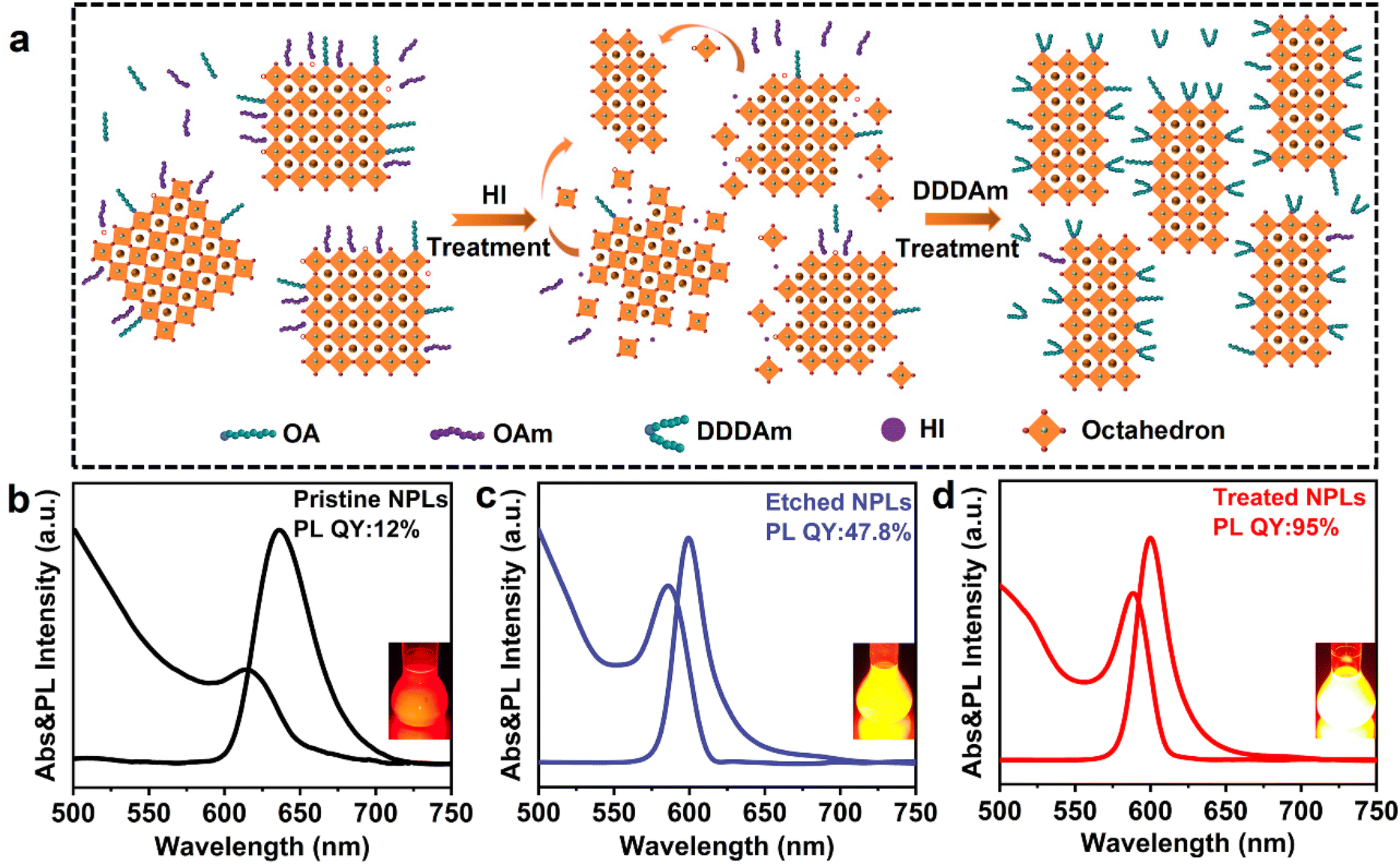 | ||
| Fig. 1 HI-assisted ligand treatment method for the synthesis of CsPbI3 NPLs. (a) Schematic outlines the synthesis strategy. (b–d) Absorption and PL spectra of (b) pristine CsPbI3 NPLs, (c) etched CsPbI3 NPLs using HI, and (c) treated CsPbI3 NPLs using HI and the DDDAm ligand. The insets display digital photos of colloidal solutions on these NPLs under 365 nm UV lamp excitation. | ||
To examine the impact of in situ etching with HI and surface modification with short-chain DDDAm ligands on the morphology of CsPbI3 NPLs, we conducted characterization using transmission electron microscopy (TEM) technology on the pristine, etched, and treated NPLs. The TEM image reveals that pristine CsPbI3 exhibits a hexagonal NPL morphology (Fig. 2a), with an average size of 23.78 nm. Upon the introduction of HI, the pristine CsPbI3 NPLs underwent a regular arrangement, and the NPLs’ width was observed as 2 nm (Fig. 2b), indicating that the prepared NPLs consisted of 3 monolayers,46 consistent with their absorption and PL characteristics. Notably, this regular arrangement of NPLs typically occurs in high-quality NPLs, possibly due to the self-assembly induced by HI etching of incomplete octahedra on the surface of CsPbI3.41 Following the addition of DDDAm, there was no significant change in the morphology of the treated NPLs (Fig. 2c), aligning with the observation that the PL spectrum remained unchanged after adding DDDAm. High-resolution TEM images (Fig. 2d–f) indicate that the lattice spacing of the three types of NPLs is 0.32 nm, consistent with the lattice spacing of the (002) crystal plane of the α-CsPbI3 phase,47 suggesting that the crystal structure of the NPLs remained unaltered during etching and ligand treatment. These results imply that the crystal structure and morphology of the NPLs were preserved throughout the synthesis process with HI-assisted ligand treatment, contributing to the production of CsPbI3 NPLs with good PL properties.
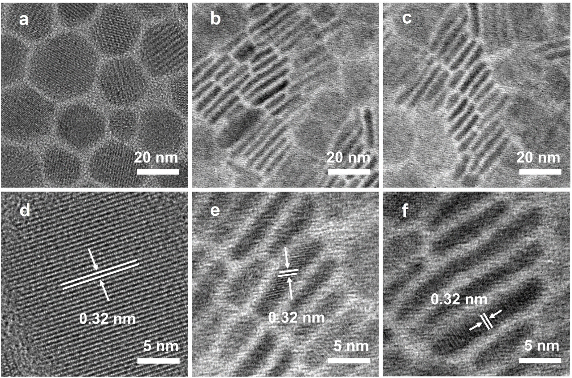 | ||
| Fig. 2 Morphology of CsPbI3 NPLs during the HI-assisted ligand treatment process. TEM images of (a) pristine, (b) etched, and (c) treated NPLs. High-resolution TEM images of (d) pristine, (e) etched, and (f) treated NPLs. | ||
Fig. 3a displays the X-ray diffraction (XRD) pattern of the pristine, etched, and treated CsPbI3 NPLs. The pristine CsPbI3 NPLs exhibit distinct diffraction features consistent with known α-CsPbI3.20,47 In contrast, both etched and treated NPLs show XRD diffraction peaks with apparent periodicity (Fig. S7 and Table S1, ESI†). Calculation using Bragg's equation reveals a corresponding interlayer spacing of 5.1 nm for these NPLs, consistent with the sum of the thickness of CsPbI3 NPLs and the size of surface ligands (OA/OAm) as shown in TEM observation. Such periodic diffraction is typically reported in high-quality NPLs,48 suggesting self-assembly induced by HI etching of incomplete octahedra on the NPLs’ surface. This implies that CsPbI3 NPLs synthesized through HI-assisted ligand treatment exhibit excellent crystallinity.
 | ||
| Fig. 3 The microstructure of the pristine, etched, and treated CsPbI3 NPLs. (a) XRD patterns. (b) FTIR spectra. (c) N 1s, (d) Cs 3d, (e) Pb 4f, and (f) I 3d of XPS spectra. | ||
To investigate the impact of in situ HI etching and short-chain DDDAm ligand modification on the surface states of CsPbI3 NPLs, Fourier-transform infrared (FTIR) spectroscopy was conducted on these CsPbI3 NPLs (Fig. 3b). For pristine NPLs, two stretching peaks at 1820 and 1570 cm−1, attributed to C![[double bond, length as m-dash]](https://www.rsc.org/images/entities/char_e001.gif) O and –COO− vibrations, are observed.49 Additionally, a signal from the N–H bending vibration of amine functional groups is noted at 1624 cm−1, indicating the presence of abundant OA and OAm ligands on the pristine NPLs’ surface.49,50 In etched NPLs, the absorption peaks related to hydrocarbon groups (2798–3045 cm−1 and 1454 cm−1) and OA/OAm are significantly reduced, suggesting the removal of organic ligands after HI etching. For the treated NPLs, it exhibits a prominent N–H signal,49 indicating effective coordination of DDDAm with the NPLs’ surface and efficient passivation of surface defects.
O and –COO− vibrations, are observed.49 Additionally, a signal from the N–H bending vibration of amine functional groups is noted at 1624 cm−1, indicating the presence of abundant OA and OAm ligands on the pristine NPLs’ surface.49,50 In etched NPLs, the absorption peaks related to hydrocarbon groups (2798–3045 cm−1 and 1454 cm−1) and OA/OAm are significantly reduced, suggesting the removal of organic ligands after HI etching. For the treated NPLs, it exhibits a prominent N–H signal,49 indicating effective coordination of DDDAm with the NPLs’ surface and efficient passivation of surface defects.
To further investigate the influence of HI in situ etching and DDDAm ligand modification on the surface atomic coordination environment of CsPbI3 NPLs, X-ray photoelectron spectroscopy (XPS) characterization was conducted on these NPLs (Fig. 3c). For pristine NPLs, only one N peak is detected at 401.7 eV, confirming the presence of protonated amine −NH3+,49 likely originating from proton exchange between OAm and OA. After the addition of HI, the intensity of the –NH3+ signal significantly decreases,49 and another signal peak appears at 401.1 eV, indicating the removal of OA and the formation of a non-protonated amine (NH2). The treated NPLs with surface ligand modification show a substantial enhancement of the NH2 signal at 401.1 eV,51,52 associated with the non-protonated amine of DDDAm. The binding energy of Cs 3d shows no significant changes after HI in situ etching and DDDAm treatment (Fig. 3d). Upon the addition of HI, the binding energies of Pb 4f shift from the initial 142.05 eV and 137.2 eV (pristine CsPbI3) to 142.3 eV and 137.45 eV (etched CsPbI3), and I 3d binding energies change from the original 629.3 eV and 617.8 eV (pristine NPLs) to 629.7 eV and 618.2 eV (etched NPLs). This is attributed to the enhancement of chemical bonds between Pb2+ and I− in the surface octahedron [PbI6]4− due to the introduction of HI and excess I− ions. Following the addition of DDDAm, the Pb 4f binding energy increases by 0.1 eV, and the I 3d binding energy increases by 0.3 eV,53 indicating the strengthening of the interaction between DDDAm and I− ions, influencing the chemical environment around them.41,49 These results further confirm that HI in situ etching removed the octahedral [PbI6]4− and assisted in bridging strong L-shaped coordination with DDDAm on the surface of NPLs, effectively passivating the surface defects of the CsPbI3 NPLs and enhancing their optical properties.
It is reported that CsPbI3 NPLs typically exhibit a significant tail emission due to strong quantum confinement effects, believed to be caused by many defects.54,55 In our study, after in situ etching with HI and ligand treatment, the wavelength blue shift and asymmetry in the long-wavelength region of CsPbI3 NPLs were effectively suppressed, indicating a reduction in iodine vacancy defects. To further clarify this point, the Urbach energy (EU) of these NPLs was calculated by plotting the absorption coefficient as a function of photon energy. Generally, the defect density of semiconductors is positively correlated with EU, meaning that samples with more defects exhibit a larger EU.56 The EU values of the pristine, etched, and treated NPLs are shown in Fig. 4a based on the fitting curve of the absorption spectra. The calculation results show that the EU value of pristine NPLs is 43.48 meV. After the introduction of HI, the EU value of the etched NPLs decreased to 19.23 meV, indicating that HI etched the incomplete octahedra on the surface of CsPbI3, and iodine ions reduced the iodine vacancy defects in the NPLs. The treated NPLs with DDDAm ligands showed a decrease in EU value from 19.23 meV to 15.87 meV, indicating that the addition of DDDAm further passivated the surface defects of CsPbI3 NPLs and reduced their defect density. These results confirm that in situ HI etching and DDDAm ligand modification strategies can effectively slow down the defect states on the surface of CsPbI3 NPLs and improve their optical properties.
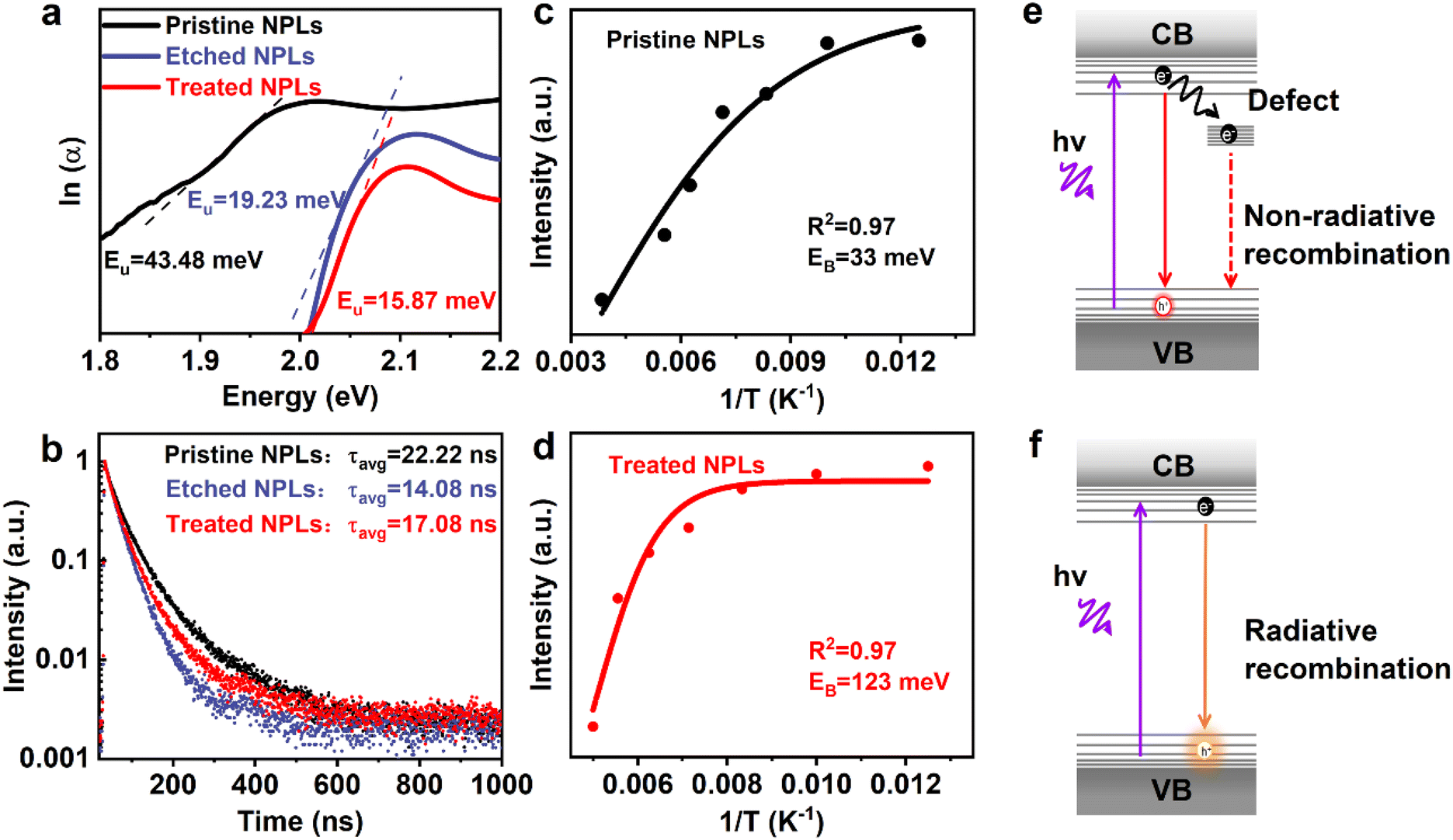 | ||
| Fig. 4 The photophysical properties of CsPbI3 NPLs. (a) Urbach energy spectra and (b) PL decay curves of the pristine, etched, and treated NPLs. (c and d) The function and fitting curve of the reciprocal of the PL intensity and temperature for both the pristine and treated NPLs. (e and f) Schematic representations of the PL radiative recombination process for the pristine and treated NPLs. | ||
To understand the impact of in situ etching with HI and ligand passivation on the radiative recombination of CsPbI3 NPLs, we obtained the PL decay curves of these NPLs as shown in Fig. 4b. The fitted results (Table S2, ESI†) illustrate that the average lifetime (τavg) decreased from 22.22 ns in the pristine NPLs to 14.08 ns in the etched NPLs after the addition of HI etching.46 This decrease is attributed to the introduction of defects caused by HI etching of incomplete octahedra on the CsPbI3 surface and the removal of the ligand OA/OAm on the etched NPL surface. Following the introduction of DDDAm, the average lifetime of the treated NPLs increased to 17.08 ns, indicating that DDDAm further passivated defects on the NPL surface.43 By measuring PL QY and average lifetime data, we calculated the non-radiative rate (knr) using the formula:43

The calculated results shown in Table S2 (ESI)† revealed that, compared to the untreated pristine NPLs, the knr of the etched NPLs was significantly reduced, suggesting that in situ HI etching and DDDAm ligand modification strategies effectively inhibit the non-radiative recombination process of CsPbI3 NPLs.
Temperature-dependent PL spectroscopy (Fig. S8, ESI†) was also conducted on both the pristine and treated NPL samples to gain insight into HI-assisted ligand treatment on the PL recombination of the NPLs. Fig. 4c and d depict the relationship between the integrated strength and temperature of the NPLs, which can be fitted using the following formula:56

Here, I(T) is the PL strength at different temperatures, I0 is the strength at 0 K, Eb is the exciton binding energy, and kB is the Boltzmann constant. The results indicated that the exciton binding energy of the treated NPLs was 123 meV, significantly higher than that of the pristine NPLs at 33 meV. This finding further substantiates that in situ etching and ligand passivation can reduce iodine vacancy defects in CsPbI3 NPLs, diminish shallow electron traps, and address the under-coordination of surface Pb atoms. The corresponding PL recombination process in the treated NPLs before and after treatment is shown in Fig. 4e and f. It is found that the introduction of HI in situ etching and DDDAm ligand modification results in the removal of most surface defects originating from iodine vacancies by HI. Simultaneously, HI introduced excessive iodine ions and DDDAm ligands to fill these trap states, leading to a reduction in non-radiative recombination and a significant increase in radiative recombination. This enhancement in radiative recombination ultimately contributes to the improved PL QY of CsPbI3 NPLs.
Next, we tested the stability of CsPbI3 NPLs through our HI-assisted ligand treatment. These NPLs were placed in n-hexane solution under ambient conditions (temperature 27 ± 5 °C, humidity 70 ± 20%) for 21 days to assess changes in their PL properties and crystal structure. Fig. 5a shows digital photos of pristine and treated NPLs before and after 21 days. It can be observed that the solution of pristine CsPbI3 NPLs changed from red to yellow with partial precipitation, while the treated CsPbI3 NPLs showed no significant color change. The corresponding PL tests indicated that the treated CsPbI3 NPLs maintained 91% PL QY after 21 days, whereas the pristine CsPbI3 NPLs lost their luminescence properties as shown in Fig. 5b. Specifically, the treated CsPbI3 NPLs maintained a PL QY of 61.8% even after 87 days under ambient conditions (see Fig. S9, ESI†), exhibiting outstanding stability, as shown in Table S3 (ESI).† It can be observed that the XRD patterns (Fig. 5c and d) of the treated CsPbI3 NPLs showed no significant change after 21 days, while the XRD pattern of the pristine CsPbI3 NPLs involved from the α-phase to the yellow δ-phase,57 confirming the transformation of its solution from the luminescent perovskite phase to the non-luminescent yellow phase. We tested the stability of both the pristine and treated NPL films after one week of ambient storage (Fig. S10, ESI†). The film with pristine NPLs exhibited a continuous red-shift in the PL peak position, along with a gradual decrease in PL intensity. In contrast, the treated NPL film maintained a stable PL peak position with no significant shift, and the PL intensity remained at 61.4% of the original level. This suggests enhanced stability in the treated NPL films compared to those with the pristine NPLs. We also monitored the PL evolution process of both types of NPLs at different power levels (Fig. 5e, f and Fig. S11, ESI†). Notably, the emission center of the pristine CsPbI3 NPLs continuously shifted towards longer wavelengths even at the lowest power of 100 mW cm−2, while the emission peak of the treated CsPbI3 NPLs did not show a significant shift, even at the highest power of 500 mW cm−2. The excellent spectral stability of the treated CsPbI3 NPLs is attributed to the strong coordination of DDDAm on the NPL surface assisted by HI, inhibiting fusion between NPLs. This suggests that the in situ HI etching and DDDAm ligand modification strategy effectively enhances the stability of CsPbI3 NPLs.
 | ||
| Fig. 5 The stability of CsPbI3 NPLs. (a) Digital photos of the pristine and treated NPLs before and after 21 days of exposure to environmental conditions, and (b) the corresponding PL QY variation curves. (c and d) XRD patterns of the pristine (c) and treated (d) NPLs before and after 21 days of exposure to environmental conditions. (e and f) 2D pseudo color PL spectral evolution of the pristine (e) and treated (f) NPLs under continuous 365 nm UV light irradiation for 1 h. | ||
To evaluate the potential application of CsPbI3 NPLs prepared through in situ etching with HI and passivation using DDDAm ligands in optoelectronic devices, we fabricated a PeLED utilizing the treated CsPbI3 NPLs as the emission layer. The device structure is composed of ITO/PEDOT:PSS/Poly TPD/CsPbI3/TPBi/LiF/Al, as depicted in Fig. 6a. This PeLED exhibits bright EL with an emission center at 600 nm and a FWHM of 23 nm, along with CIE coordinates of (0.60, 0.35) (Fig. S12, ESI†). Notably, as the operational voltage of the PeLED increases, there is no significant shift in the EL peak position (Fig. 6b). This suggests that the strategies involving HI in situ etching and DDDAm ligand modification substantially enhance the stability of the CsPbI3 NPLs. In Fig. 6c, it is demonstrated that the PeLED achieves a maximum brightness of 472.85 cd m−2 at a current density of 31.2 mA cm−2, accompanied by a peak EQE of 2.98% (Fig. 6d) and a luminous efficiency of 7.18 cd A−1 (Fig. S14, ESI†). Even when the brightness exceeds 100 cd m−2, the EQE remains at 2.36% (Fig. S13, ESI†). This performance is comparable to that of NPL-based PeLEDs reported in the literature (Table S4, ESI†), suggesting promising application prospects for CsPbI3 NPLs prepared through HI in situ etching and DDDAm ligand modification strategies in optoelectronic devices.
 | ||
| Fig. 6 EL performance of PeLEDs based on the treated CsPbI3 NPLs. (a) Structure and (b) EL spectra of PeLEDs under different voltage drivings. (c) Current density–brightness–voltage relationship, and (d) EQE–brightness relationship of PeLEDs. | ||
3. Conclusion
In conclusion, we have demonstrated a HI-assisted ligand treatment strategy for the preparation of near-unity QY and highly stable CsPbI3 NPLs. Our study reveals that HI can etch away incomplete octahedral facets on the surface of the NPLs, while the introduced short-chain DDDAm ligands effectively passivate surface defects and enhance the stability. The CsPbI3 NPLs prepared through this strategy exhibit a high PL QY of 95%, and even after 21 days of exposure to environmental conditions, the PL QY remains at 91%, maintaining a remarkable 61.8% after 87 days. The PeLED device based on CsPbI3 NPLs achieves a peak EQE of 2.98%, maintaining an EQE of 2.36% at a high brightness of 100 cd m−2, showing excellent EL performance. This efficient synthesis strategy, utilizing HI-assisted ligand treatment, is expected to be applicable to the synthesis of other perovskite NPLs, facilitating the broader integration of perovskite NPLs in optoelectronic technology.Author contributions
S. C., B. Z., and J. Z. supervised this work. S. C. and Z. L. conceptualized and designed the experiments. Z. L., K. X., and Z. D. carried out the main experimental work, including materials synthesis, optical characterizations, data analysis. Y. S. conducted the fabrication of PeLEDs and the related performance tests. S. C., Z. L., and Y. S. co-wrote the manuscript. All authors were involved in the results discussion and manuscript preparation.Conflicts of interest
The authors declare no conflict of interest.Acknowledgements
This work was supported by the Outstanding Youth Fund of the Guangxi Natural Science Foundation (2022GXNSFFA035032), the National Natural Science Foundation of China (62165001, 12174075), the special fund for “Guangxi Bagui Scholars”, and the “Guangxi Hundred-Talent Program”. The Center for Instrumental Analysis of Guangxi University is acknowledged for providing research facilities and resources for the experiments.References
- Y. Cao, N. Wang, H. Tian, J. Guo, Y. Wei, H. Chen, Y. Miao, W. Zou, K. Pan, Y. He, H. Cao, Y. Ke, M. Xu, Y. Wang, M. Yang, K. Du, Z. Fu, D. Kong, D. Dai, Y. Jin, G. Li, H. Li, Q. Peng, J. Wang and W. Huang, Perovskite light-emitting diodes based on spontaneously formed submicrometre-scale structures, Nature, 2018, 562, 249–253 CrossRef CAS PubMed
.
- C. de Weerd, L. Gomez, A. Capretti, D. M. Lebrun, E. Matsubara, J. Lin, M. Ashida, F. C. M. Spoor, L. D. A. Siebbeles, A. J. Houtepen, K. Suenaga, Y. Fujiwara and T. Gregorkiewicz, Efficient carrier multiplication in CsPbI3 perovskite nanocrystals, Nat. Commun., 2018, 9, 4199 CrossRef PubMed
- G. Rainò, N. Yazdani, S. C. Boehme, M. Kober-Czerny, C. Zhu, F. Krieg, M. D. Rossell, R. Erni, V. Wood, I. Infante and M. V. Kovalenko, Ultra-narrow room-temperature emission from single CsPbBr3 perovskite quantum dots, Nat. Commun., 2022, 13, 2587 CrossRef PubMed
- D. Ma, K. Lin, Y. Dong, H. Choubisa, A. H. Proppe, D. Wu, Y.-K. Wang, B. Chen, P. Li, J. Z. Fan, F. Yuan, A. Johnston, Y. Liu, Y. Kang, Z.-H. Lu, Z. Wei and E. H. Sargent, Distribution control enables efficient reduced-dimensional perovskite LEDs, Nature, 2021, 599, 594–598 CrossRef CAS PubMed
- Y. Wang, Y. Teng, P. Lu, X. Shen, P. Jia, M. Lu, Z. Shi, B. Dong, W. W. Yu and Y. Zhang, Low roll–off perovskite quantum dot light–emitting diodes achieved by augmenting hole mobility, Adv. Funct. Mater., 2020, 30, 1910140 CrossRef CAS
- T. Chen, Q. Yang, P. Zhang, R. Chen, Y. Lin, W. Zhou, L. Sui, X. Zheng, G. Chen and F. Li, Stapled ligand for synthesis of highly emissive and stable CsPbBr3 perovskite nanocrystals in polar organic solvent, Inorg. Chem. Front., 2023, 10, 5303–5310 RSC
- J. He, X. Zhang, C. Xie, H. S. Chen and P. Yang, CsPbX3 nanocrystals embedded in hollow AlO(OH) nanosheet assemblies towards highly bright flexible multicolor emitting films, J. Mater. Chem. C, 2023, 11, 7654–7661 RSC
- K. Wang, Z. Jin, L. Liang, H. Bian, D. Bai, H. Wang, J. Zhang, Q. Wang and S. Liu, All-inorganic cesium lead iodide perovskite solar cells with stabilized efficiency beyond 15%, Nat. Commun., 2018, 9, 4544 CrossRef PubMed
- C. Yi, C. Liu, K. Wen, X.-K. Liu, H. Zhang, Y. Yu, N. Fan, F. Ji, C. Kuang, B. Ma, C. Tu, Y. Zhang, C. Xue, R. Li, F. Gao, W. Huang and J. Wang, Intermediate-phase-assisted low-temperature formation of γ-CsPbI3 films for high-efficiency deep-red light-emitting devices, Nat. Commun., 2020, 11, 4736 CrossRef CAS PubMed
- X. Hu, Y. Xu, J. Wang, J. Ma, L. Wang and W. Jiang, Ligand-modified synthesis of shape-controllable and highly luminescent CsPbBr3 perovskite nanocrystals under ambient conditions, Inorg. Chem. Front., 2022, 9, 6080–6090 RSC
- H. Wu, J. Qiu, J. Wang, Y. Wen, Q. Wang, Z. Long, D. Zhou, Y. Yang and D. Wang, The dual-defect passivation role of lithium bromide doping in reducing the nonradiative loss in CsPbX3 (X = Br and I) quantum dots, Inorg. Chem. Front., 2021, 8, 658–668 RSC
- Y.-C. Yang, Y.-W. Peng, A.-T. Lee, G. Kumar and M. H. Huang, CsPbBr3 and CsPbI3 rhombic dodecahedra and nanocubes displaying facet-dependent optical properties, Inorg. Chem. Front., 2021, 8, 4685–4695 RSC
- Q. Wang, X. Wang, Z. Yang, N. Zhou, Y. Deng, J. Zhao, X. Xiao, P. Rudd, A. Moran, Y. Yan and J. Huang, Efficient sky-blue perovskite light-emitting diodes via photoluminescence enhancement, Nat. Commun., 2019, 10, 5633 CrossRef CAS PubMed
- X.-K. Liu, W. Xu, S. Bai, Y. Jin, J. Wang, R. H. Friend and F. Gao, Metal halide perovskites for light-emitting diodes, Nat Mater., 2020, 20, 10–21 CrossRef PubMed
- W. Shi, X. Zhang, H. S. Chen, K. Matras-Postolek and P. Yang, Zn-derived ligand engineering towards stable and bright CsPbI3 nanocrystals for white emitting, J. Mater. Chem. C, 2022, 10, 13117–13123 RSC
- Z. Dai, J. Chen and B. Yang, Yb2+-alloyed Cs4PbI6−CsPbI3 perovskite nanocomposites for efficient and stable pure-red emission, J. Phys. Chem. Lett., 2021, 12, 10093–10098 CrossRef CAS PubMed
- W. Shi, X. Zhang, K. Matras-Postolek and P. Yang, Mn-derived Cs4PbX6 nanocrystals with stable and tunable wide luminescence for white light-emitting diodes, J. Mater. Chem. C, 2022, 10, 3886–3893 RSC
- Y. Wu, C. Wei, X. Li, Y. Li, S. Qiu, W. Shen, B. Cai, Z. Sun, D. Yang, Z. Deng and H. Zeng, In situ passivation of PbBr64– octahedra toward blue luminescent CsPbBr3 nanoplatelets with near 100% absolute quantum yield, ACS Energy Lett., 2018, 3, 2030–2037 CrossRef CAS
- H. Huang, M. I. Bodnarchuk, S. V. Kershaw, M. V. Kovalenko and A. L. Rogach, Lead halide perovskite nanocrystals in the research spotlight: stability and defect tolerance, ACS Energy Lett., 2017, 2, 2071–2083 CrossRef CAS PubMed
- J. Hu, C. Bi, X. Zhang, Y. Lu, W. Zhou, Z. Zheng, Y. Tang, F. Lu, Z. Yao, B. Tian, X. Wang, K. Selvakumar, J. Tian and M. Sui, Yellow-light emitted single halide CsPbI3 nanowire, Appl. Mater. Today, 2022, 29, 101592 CrossRef
- M. Imran, V. Caligiuri, M. Wang, L. Goldoni, M. Prato, R. Krahne, L. De Trizio and L. Manna, Benzoyl halides as alternative precursors for the colloidal synthesis of lead-based halide perovskite nanocrystals, J. Am. Chem. Soc., 2018, 140, 2656–2664 CrossRef CAS
- F. Liu, Y. Zhang, C. Ding, S. Kobayashi, T. Izuishi, N. Nakazawa, T. Toyoda, T. Ohta, S. Hayase, T. Minemoto, K. Yoshino, S. Dai and Q. Shen, Highly luminescent phase-stable CsPbI3 perovskite quantum dots achieving near 100% absolute photoluminescence quantum yield, ACS Nano, 2017, 11, 10373–10383 CrossRef CAS PubMed
- M. Lai, Q. Kong, C. G. Bischak, Y. Yu, L. Dou, S. W. Eaton, N. S. Ginsberg and P. Yang, Structural, optical, and electrical properties of phase-controlled cesium lead iodide nanowires, Nano Res., 2017, 10, 1107–1114 CrossRef CAS
- M. Zhang, C. Bi, Y. Xia, X. Sun, X. Wang, A. Liu, S. Tian, X. Liu, N. H. de Leeuw and J. Tian, Water–driven synthesis of deep–blue perovskite colloidal quantum wells for electroluminescent devices, Angew. Chem., Int. Ed., 2023, 62, 202300149 CrossRef PubMed
- W. Shi, X. Zhang, C. Xie, H. S. Chen and P. Yang, Blue emitting CsPbBr3: high quantum confinement effect and well–adjusted shapes (nanorods, nanoplates, and cubes) toward white light emitting diodes, Adv. Opt. Mater., 2023, 11, 202302129 Search PubMed
- C. Xie, X. Zhang, H. S. Chen and P. Yang, Synthesis–kinetics of violet– and blue–emitting perovskite nanocrystals with high brightness and superior stability toward flexible conversion layer, Small, 2023, 19, 2308896 CrossRef
- F. Ke, C. Wang, C. Jia, N. R. Wolf, J. Yan, S. Niu, T. P. Devereaux, H. I. Karunadasa, W. L. Mao and Y. Lin, Preserving a robust CsPbI3 perovskite phase via pressure-directed octahedral tilt, Nat. Commun., 2021, 12, 461 CrossRef CAS PubMed
- P. Luo, W. Xia, S. Zhou, L. Sun, J. Cheng, C. Xu and Y. Lu, Solvent engineering for ambient-air-processed, phase-stable CsPbI3 in perovskite solar cells, J. Phys. Chem. Lett., 2016, 7, 3603–3608 CrossRef CAS PubMed
- Y. Wang, G. Chen, D. Ouyang, X. He, C. Li, R. Ma, W. J. Yin and W. C. H. Choy, High phase stability in CsPbI3 enabled by Pb–I octahedra anchors for efficient inorganic perovskite photovoltaics, Adv. Mater., 2020, 32, 2000186 CrossRef CAS PubMed
- Y. Wang, Y. Chen, T. Zhang, X. Wang and Y. Zhao, Chemically stable black phase CsPbI3 inorganic perovskites for high–efficiency photovoltaics, Adv. Mater., 2020, 32, 2001025 CrossRef CAS
- Q. A. Akkerman, S. G. Motti, A. R. Srimath Kandada, E. Mosconi, V. D'Innocenzo, G. Bertoni, S. Marras, B. A. Kamino, L. Miranda, F. De Angelis, A. Petrozza, M. Prato and L. Manna, Solution synthesis approach to colloidal cesium lead halide perovskite nanoplatelets with monolayer-level thickness control, J. Am. Chem. Soc., 2016, 138, 1010–1016 CrossRef CAS PubMed
- C. Otero-Martínez, J. Ye, J. Sung, I. Pastoriza-Santos, J. Pérez-Juste, Z. Xia, A. Rao, R. L. Z. Hoye and L. Polavarapu, Colloidal metal–halide perovskite nanoplatelets: thickness–controlled synthesis, properties, and application in light–emitting diodes, Adv. Mater., 2022, 34, 2107105 CrossRef PubMed
- X. Zhang and P. Yang, CsPbX3 (X = Cl, Br, and I) nanocrystals in substrates toward stable photoluminescence: nanoarchitectonics, properties, and applications, Langmuir, 2023, 39, 11188–11212 CrossRef CAS
- B. Han, B. Cai, Q. Shan, J. Song, J. Li, F. Zhang, J. Chen, T. Fang, Q. Ji, X. Xu and H. Zeng, Stable, efficient red perovskite light–emitting diodes by (α, δ)–CsPbI3 phase engineering, Adv. Funct. Mater., 2018, 28, 1804285 CrossRef
- S. Wang, J. Jin, Y. Qi, P. Liu, Y. Xia, Y. Jiang, R. X. He, B. Chen, Y. Liu and X. Z. Zhao,
δ–CsPbI3 intermediate phase growth assisted sequential deposition boosts stable and high–efficiency triple cation perovskite solar cells, Adv. Funct. Mater., 2019, 30, 1908343 CrossRef
- Y. Yin, H. Cheng, W. Tian, M. Wang, Z. Yin, S. Jin and J. Bian, Self-assembled δ-CsPbI3 nanowires for stable white light emission, ACS Appl. Nano Mater., 2022, 5, 18879–18884 CrossRef CAS
- J. T. Griffiths, F. W. Rocca Rivarola, N. J. L. K. Davis, R. Ahumada-Lazo, J. A. Alanis, P. Parkinson, D. J. Binks, W. Y. Fu, F. De La Pena, M. B. Price, A. Howkins, I. Boyd, C. J. Humphreys, N. C. Greenham and C. Ducati, Effect of size on the luminescent efficiency of perovskite nanocrystals, ACS Appl. Energy Mater., 2019, 2, 6998–7004 CrossRef CAS
- Y. Shen, L. P. Cheng, Y. Q. Li, W. Li, J. D. Chen, S. T. Lee and J. X. Tang, High–efficiency perovskite light–emitting diodes with synergetic outcoupling enhancement, Adv. Mater., 2019, 31, 1901517 CrossRef PubMed
- H. Wang, X. Zhang, Q. Wu, F. Cao, D. Yang, Y. Shang, Z. Ning, W. Zhang, W. Zheng, Y. Yan, S. V. Kershaw, L. Zhang, A. L. Rogach and X. Yang, Trifluoroacetate induced small-grained CsPbBr3 perovskite films result in efficient and stable light-emitting devices, Nat. Commun., 2019, 10, 665 CrossRef CAS PubMed
- H. E. Sánchez-Godoy, E. A. Erazo, A. F. Gualdrón-Reyes, A. H. Khan, S. Agouram, E. M. Barea, R. A. Rodriguez, I. Zarazúa, P. Ortiz, M. T. Cortés, V. Muñoz-Sanjosé, I. Moreels, S. Masi and I. Mora-Seró, Preferred growth direction by PbS nanoplatelets preserves perovskite infrared light harvesting for stable, reproducible, and efficient solar cells, Adv. Energy Mater., 2020, 10, 2002422 CrossRef
- Z. Shen, S. Zhao, D. Song, Z. Xu, B. Qiao, P. Song, Q. Bai, J. Cao, G. Zhang and W. Swelm, Improving the quality and luminescence performance of all–inorganic perovskite nanomaterials for light–emitting devices by surface engineering, Small, 2020, 16, 1907089 CrossRef CAS PubMed
- C. Zhang, Q. Wan, B. Wang, W. Zheng, M. Liu, Q. Zhang, L. Kong and L. Li, Surface ligand engineering toward brightly luminescent and stable cesium lead halide perovskite nanoplatelets for efficient blue-light-emitting diodes, J. Phys. Chem. C, 2019, 123, 26161–26169 CrossRef CAS
- Q. Chen, S. Cao, K. Xing, M. Ning, R. Zeng, Y. Wang and J. Zhao, Mg2+-assisted passivation of defects in CsPbI3 perovskite nanocrystals for high-efficiency photoluminescence, J. Phys. Chem. Lett., 2021, 12, 11090–11097 CrossRef CAS PubMed
- C. Otero-Martínez, D. García-Lojo, I. Pastoriza-Santos, J. Pérez-Juste and L. Polavarapu, Dimensionality control of inorganic and hybrid perovskite nanocrystals by reaction temperature: from no–confinement to 3D and 1D quantum confinement, Angew. Chem., Int. Ed., 2021, 60, 26677–26684 CrossRef
- S. Shin, N. Gwak, H. Yoo, H. Jang, M. Lee, K. Kang, S. Kim, S. Yeon, T. Ann Kim, S. Kim, G. W. Hwang and N. Oh, Fluoride-free synthesis strategy for luminescent InP cores and effective shelling processes via combinational precursor chemistry, Chem. Eng. J., 2023, 466, 143223 CrossRef CAS
- Y. Tong, E. Bladt, M. F. Aygüler, A. Manzi, K. Z. Milowska, V. A. Hintermayr, P. Docampo, S. Bals, A. S. Urban, L. Polavarapu and J. Feldmann, Highly luminescent cesium lead halide perovskite nanocrystals with tunable composition and thickness by ultrasonication, Angew. Chem., Int. Ed., 2016, 55, 13887–13892 CrossRef CAS PubMed
- C. Bi, J. Hu, Z. Yao, Y. Lu, D. Binks, M. Sui and J. Tian, Self–assembled perovskite nanowire clusters for high luminance red light–emitting diodes, Adv. Funct. Mater., 2020, 30, 2005990 CrossRef CAS
- B. Bai, C. Zhang, Y. Dou, L. Kong, L. Wang, S. Wang, J. Li, Y. Zhou, L. Liu, B. Liu, X. Zhang, I. Hadar, Y. Bekenstein, A. Wang, Z. Yin, L. Turyanska, J. Feldmann, X. Yang and G. Jia, Atomically flat semiconductor nanoplatelets for light-emitting applications, Chem. Soc. Rev., 2023, 52, 318–360 RSC
- C. Bi, Z. Yao, X. Sun, X. Wei, J. Wang and J. Tian, Perovskite quantum dots with ultralow trap density by acid etching–driven ligand exchange for high luminance and stable pure–blue light–emitting diodes, Adv. Mater., 2021, 33, 2006722 CrossRef CAS PubMed
- M. Xie, J. Guo, X. Zhang, C. Bi, X. Sun, H. Li, L. Zhang, D. Binks, G. Li, W. Zheng and J. Tian, Suppressing ion migration of mixed–halide perovskite quantum dots for high efficiency pure-red light–emitting diodes, Adv. Funct. Mater., 2023, 33 Search PubMed
- Y.-H. Kim and T.-W. Lee, Engineering colloidal perovskite nanocrystals and devices for efficient and large-area light-emitting diodes, Acc. Mater. Res., 2023, 4, 655–667 CrossRef CAS
- A. Liu, C. Bi and J. Tian, All solution–processed high performance pure–blue perovskite quantum–dot light–emitting diodes, Adv. Funct. Mater., 2022, 32, 2207069 CrossRef CAS
- Z. Yang, X. Yuan, Y. Song, M. Chen, K. Xing, S. Cao, J. Zheng and J. Zhao, Thickness-dependent photoluminescence properties of Mn-doped CsPbBr3 perovskite nanoplatelets synthesized at room temperature, J. Phys. Chem. C, 2023, 127, 21227–21234 CrossRef CAS
- C. M. Guvenc, Y. Yalcinkaya, S. Ozen, H. Sahin and M. M. Demir, Gd3+-doped α-CsPbI3 nanocrystals with better phase stability and optical properties, J. Phys. Chem. C, 2019, 123, 24865–24872 CrossRef CAS
- W. Zhang, Y. Ye, C. Liu, Z. Zhao, J. Wang, J. Han and X. Zhao, Revealing the effects of defects on ultrafast carrier dynamics of CsPbI3 nanocrystals in glass, J. Phys. Chem. C, 2019, 123, 15851–15858 CrossRef CAS
- Y. Song, X. Yuan, K. Xing, S. Cao, J. Zheng, B. Zou and J. Zhao, Decyl disulfide surface treatment improved photoluminescence quantum yield and stability of blue-emitting CsPbBr3 nanoplatelets, Mater. Res. Bull., 2023, 164, 112257 CrossRef CAS
- M. Chen, T. Zhang, A. Elsukova, Z. Hu, R. Zhang, Y. Wang, X. Liu, X. Liu and F. Gao, Kinetically controlled synthesis of quasi–square CsPbI3 nanoplatelets with excellent stability, Small, 2023, 2306360, DOI:10.1002/smll.202306360
Footnotes |
| † Electronic supplementary information (ESI) available. See DOI: https://doi.org/10.1039/d4qi00168k |
| ‡ Both authors contributed equally to this work. |
| This journal is © the Partner Organisations 2024 |