
Solvent-free synthetic protocols for halide perovskites
Xinrui
Zhang
a,
Jiaomao
Zheng
b,
Yifan
Wang
a,
Zhenlong
Wang
a,
Luyao
Zheng
b,
Amin
Nozariasbmarz
b,
Kai
Tao
a,
Binghe
Ma
a,
Bed
Poudel
 b,
Kai
Wang
*b and
Tao
Ye
*a
b,
Kai
Wang
*b and
Tao
Ye
*a
aMinistry of Education Key Laboratory of Micro/Nano Systems for Aerospace, Northwestern Polytechnical University, 127 Youyi Road, Xi'an 710072, China. E-mail: yetao@nwpu.edu.cn
bDepartment of Materials Science and Engineering, Pennsylvania State University, University Park, PA 16802, USA. E-mail: kqw5449@psu.edu
First published on 5th May 2023
Abstract
Halide perovskites have been extensively researched in the past decade, and explored in fields stepping out from photovoltaics towards photothermal and thermoelectric energy conversion, light-emission, high-energy electromagnetic radiation detection, memristors/artificial synapses, ferroelectricity, etc. These frontier applications will fundamentally require a benign material platform of great sample quality but easy accessibility. Traditional synthesis of halide perovskites follows a wet chemistry route, that is, dissolving–precipitation through a solution medium. However, commonly used solvents are of high-cost, environmentally unfriendly, and have high treatment complexity and low post-processing convenience. Breakthroughs on solvent toxicity minimization or even solvent exemption can pave a new roadmap to future development of perovskite-based applications. In this work, we discuss new opportunities in solvent-free synthesis including newly researched vapor deposition and mechanochemical methods, as well as other potential insights in this direction.
Introduction
Halide perovskites have attracted huge attention due to their excellent performance in various optoelectronic fields, including solar energy conversion, light-emission, high energy radiation detection, memristors/artificial synapses, ferroelectrics, photothermal conversion, thermoelectric cooling/energy generation, etc. For practical application in any device manifestations, sample quality is of paramount importance to the performance, which is fundamentally correlated to the synthetic methodology.1 The quality can be defined as features, such as lattice defects, grain size, grain boundary density, surface roughness/coverage/uniformity, topography, and crystalline orientation, of perovskites obtained from different methods, which vary significantly from sample to sample, batch to batch, and so as to the resultant performance at device level. Solution-processing methods have been the dominant synthetic methods for halide perovskite materials, with merits of low-cost, operational ease, and high compatibility for thin film manufacturing, but remaining insufficiently effective in terms of (i) solvent toxicity considerations, (ii) residual solvent induced instability issues, and (iii) timely and energetically effortful synthesis for bulk samples.2Briefly, most typically used solvents (e.g., N,N-dimethylformamide (DMF), N-methyl-2-pyrrolidone (NMP), dimethyl sulfoxide (DMSO), and N,N-dimethylacetamide (DMAC)) are of high toxicity (both DMF and DMAC are classified as substances of very high concern (SVHCs) and toxic to reproduction by the European Chemicals Agency (ECHA)), requiring additional purification techniques when considering real manufacturing at large scale.3 Secondly, high quality samples from solution methods will require complex solvent systems (including multiple aforementioned solvents as well as additional additives), which can lead to the multi-level presence of impurities, lattice distortions, and the non-uniformity of the resultant films as well as the residual solvent within the lattice which can act as a center to develop material degradation. Thirdly, for applications such as X-ray detection, thermoelectrics, and other top-down manufacturing-oriented applications, bulk samples with large volume are needed. However, solution methods make the synthesis time-inefficient because of the low crystalline growth rate and yield (low-yield (10–35%) and time-consuming (0.1–10 mm3 h−1)).4
The solution-processed methods for perovskite mainly involve two approaches, one-step deposition and two-step deposition. In one-step deposition, the perovskite formation process can be explained by the classical nucleation/growth crystallization mechanism, which includes three stages: supersaturation of the solution, nucleation, and crystal growth, which can be explained by the LaMer model (Fig. 1a).5–7 A supersaturated solution is a prerequisite for nucleation. Heating and other solvent evaporation acceleration processes can facilitate the supersaturation process to saturation (Cs). As the solvent continues to evaporate, the process of crystal nucleation begins once the solution reaches supersaturation (Cnumin), and the nucleation rate increases with increasing supersaturation. It is worth noting that once the crystal nucleus is formed, crystal growth begins immediately (Fig. 1b). In Fig. 1b, upon entering the third stage after entering supersaturation, the crystal nucleus begins to grow, and the growth rate increases sharply with increasing supersaturation concentration. Finally, as the solute is continuously consumed and the concentration drops below Cnumin, the nucleation process stops, and the crystal continues to grow. In classical nucleation theory, the nucleation rate (N) is affected by the nucleation factor (P) and the probability of atomic diffusion (G), so eqn (1) follows:
 | (1) |
 | ||
| Fig. 1 (a) Schematic nucleation and subsequent growth processes. (b) Schematic relations of the nucleation and growth rates with solute concentration. Reproduced with permission.9 Copyright 2019, Royal Society of Chemistry. (c) Schematic of the two growth mechanisms in two-step deposition methods for crystalline MAPbI3 perovskites. (i) Solid–liquid interfacial reaction mechanism at a lower MAI concentration, and (ii) dissolution–recrystallization growth mechanism at a higher MAI concentration. Reproduced with permission.8 Copyright 2015, American Chemical Society. | ||
For the two-step deposition, lead halide is first deposited on the substrate, and the organic halide subsequently infiltrates the layered lead halide crystals to react and form perovskite films. However, the concentration of the organic halide affects the depth of its infiltration into the lead halide. Previous studies investigated this and found that when the concentration of MAI is below 8 mg mL−1, the reaction proceeds according to eqn (2) and perovskite is generated in situ. When the concentration of MAI is >10 mg mL−1, MAI rapidly reacts with the surface PbI2 to form perovskite crystals, which prevents further reaction between MAI and the underlying PbI2. When the concentration of MAI further increases to above 20 mg mL−1, the surface PbI2 still undergoes reaction (eqn (2)). However, the underlying PbI2 reacts according to eqn (3) and (4), and the resulting supersaturated PbI42− recrystallizes with MA+ to form MAPbI3 perovskite (Fig. 1c).8
| PbI2(s) + MA+(sol) + I−(sol) → MAPbI3(s) | (2) |
| MAPbI3(s) + I−(sol) → MA+(sol) + PbI42−(sol) | (3) |
| PbI2(s) + 2I−(sol) → PbI42−(sol) | (4) |
The high boiling point of various solvents slows down the evaporation rate of the solvents,9 making it difficult for crystallization. A multi-solvent strategy can optimize the proceeding of the supersaturation. While on the other hand, the solute–solvent interactions are different for each precursor component and solute–solvent interactions can also alter the final product(s) composition,10–17 making the resultant film rather non-uniform. Additional solvent-related issues include (i) residual solvent in the final perovskite due to the high boiling point and strong interaction with precursor,18 (ii) solvent-induced crystal imperfection such as the presence of a large population of point defects, lattice distortion, surface traps, and grain boundaries,19–25 (iii) additional requirements for energy/effort input (that is, additional energy and procedures are needed to remove the solvent which further introduces more non-uniformity during these operations).19,26
In contrast, the “solvent-free” method can circumvent all the aforementioned issues. Compared to the mainstream solution (wet chemistry) method, the solvent-free method has been less investigated, and there are only two main methods which are classified into (i) mechanochemical synthesis and (ii) vapor-based deposition. Mechanochemical synthesis was first mentioned in 1820 by Faraday who reduced AgCl to Ag using Zn, Cu, Sn, or Fe, by grinding with a pestle in a mortar without solvent.27 Afterwards, this method was employed for large-scale preparation of pure metal clusters, supported nanoparticles, metal–organic frameworks (MOFs), and covalent organic frameworks (COFs).1 Recently, several examples of perovskite synthesis through the mechanochemical method have proposed a new solvent-free route for obtaining high-quality perovskites. The vapor-based deposition method has also been attempted due to its great reliability and reproducibility. The high vacuum environment ensures a low concentration of moisture and oxygen in the final products, effectively addressing the residual solvent issue typically encountered in solution-processed counterparts. The low moisture and oxygen concentration contributes to improved material stability, resulting in a longer device lifetime.28 Furthermore, the absence of residual solvents can potentially resolve crystal quality issues caused by solvent remnants, which have a detrimental impact on device performance. This is how in commercial organic light emitting diodes (OLEDs) the organic fluorescent dye as the active layer for the device is deposited, as solution-processing cannot perfectly solve the residual solvent-induced instability issue for the organics in industry.29
Mechanochemical synthesis method
Fig. 2 compares the solution-processed synthesis and mechanochemical synthesis methods. Taking a classic MAPbI3 (i.e., CH3NH3PbI3) as an example, in the solution-processed synthesis, the perovskite films can be formed in the spin coater within a closed chamber (Fig. 2a). After the corresponding solution is dropped onto a substrate (e.g., in a two-step method PbI2/DMF and CH3NH3/IPA (isopropyl alcohol) are sequentially dropped), the stage spinning can accelerate the solvent evaporation. In the meantime, annealing is needed to further remove the solvent in order to proceed the crystallization via the supersaturation route (Fig. 2b & c).30,31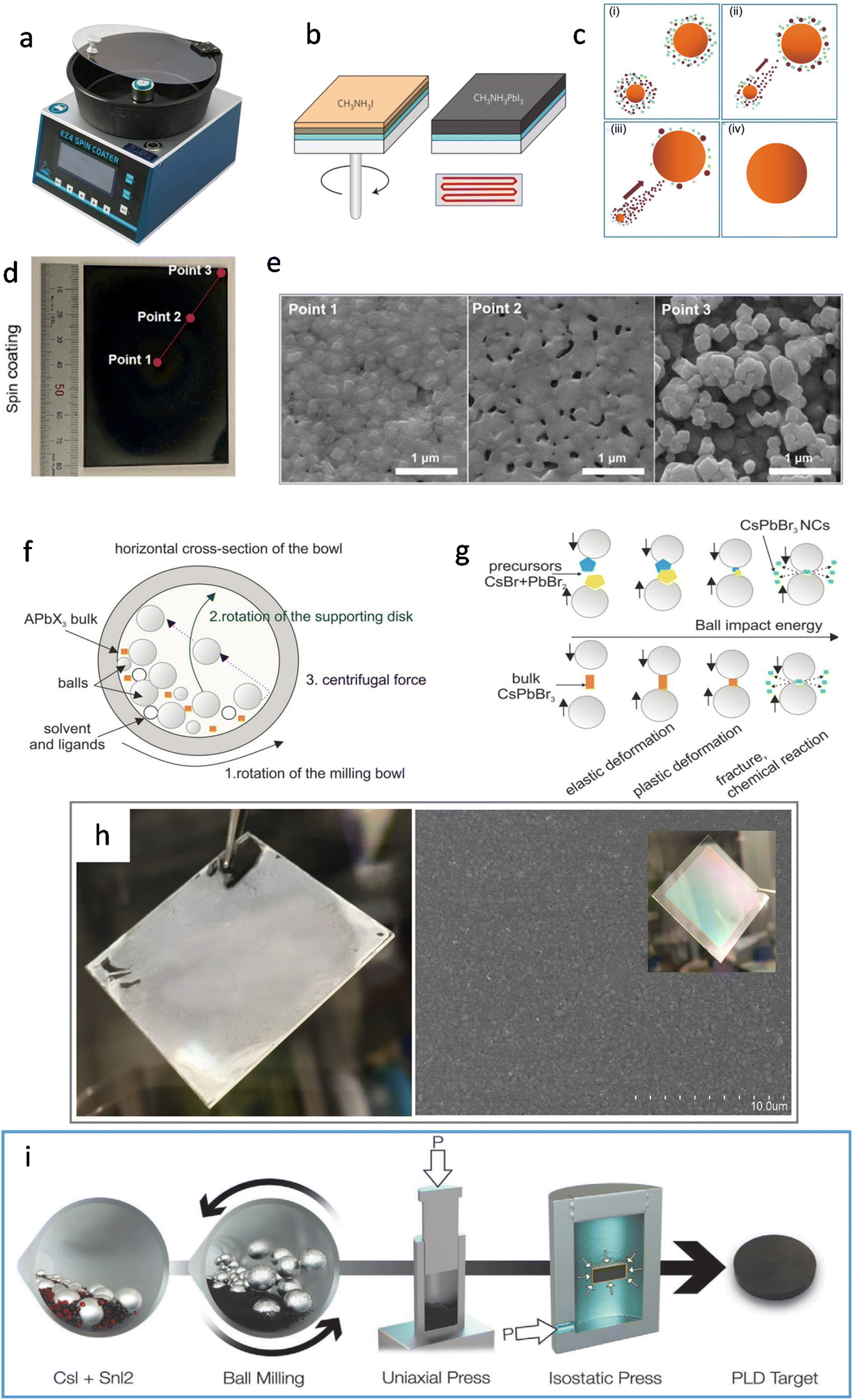 | ||
| Fig. 2 (a) Photograph of the spin coater. (b) The two-step deposition method in the solution-processed method. Reproduced with permission.31 Copyright 2014, Springer Nature. (c) Schematic of the Ostwald ripening model, showing the dynamic coarsening process of the perovskite grains with annealing time: (i) initial stage, (ii) early stage, (iii) middle stage, (iv) final stage. Reproduced with permission.30 Copyright American Chemical Society. (d) Photograph of CsPbI2Br. (e) SEM images of different locations of the thin film formed by spin coating. Reproduced with permission.32 Copyright 2021, Elsevier Inc. (f) Cross-section of a ball mill under operation. Reproduced with permission.36 Copyright 2018, American Chemical Society. (g) Schematic of processes that initiate a mechanochemical reaction. Reproduced with permission.36 Copyright 2018, American Chemical Society. (h) Photograph of spin-coated inhomogeneous Cs3Cu2I5 film (left) and SEM image and photograph (inset) of SSVD-film of Cs3Cu2I5 showing good homogeneity (right). Reproduced with permission.37 Copyright 2019, American Chemical Society. (i) Illustration of the PLD target fabrication process. From left to right: Stoichiometric mixture of CsI and SnI2 powders, ball milling, uniaxial press applying 33 MPa and hydraulic press applying 360 MPa isostatically, and final target.38 Reproduced with permission. Copyright 2020, Wiley-VCH. | ||
However, the surface uniformity of the perovskite film will be affected by the inhomogeneous solvent evaporation, nucleation, and crystal growth over the whole substrate. The larger the substrate, the greater the inhomogeneity, thus reducing the film uniformity. In Heo et al.'s work, they demonstrated the lack of uniformity in the formation of perovskite film using the spin coating technique.32 In Fig. 2d and e, SEM images of three locations from the center to the edge reveal noticeable structural irregularities in the CsPbI2Br perovskite as a function of the distance from the center of the spin-coating. This suggests that as the distance from the center increases, there is a greater variation in crystal morphology, with a higher occurrence of pinholes, ultimately resulting in reduced film uniformity. The low solubility of inorganic perovskite precursors and their rapid crystallization pose a challenge in controlling the simultaneous growth of perovskite films at different positions on a large substrate during the spin-coating process.33–35
Compared to the solution method, mechanochemical synthesis can exclude the solvent involvement throughout the whole synthesis. Fig. 2f & g show the sequential process of the traditional mechanochemical method. There are two sub-processes: ball milling and solidification. The conventional ball milling process needs a bowl and a set of grinding balls that are made of high-hardness materials (Fig. 2f). When the ball mill rotates according to a certain direction and angular velocity, the precursors are crushed by the collision of balls. At the same time, plastic/elastic deformations and eventually fractures occur, which produce dislocations that react together to form the product (Fig. 2g).36,39 By adjusting the rotation speed and the size of the grinding balls, the energy input and the size of the crystallites can be fine controlled.40 Although the all-solid-state method does not involve any solvents, the ball-milled particles usually display non-uniform sizes ranging from the nanometer-to-micrometer scales. Throughout the mechanochemical synthesis (ball-milling) process, there are still some limitations in the compatibility with film fabrication, the prepared powder is eventually dissolved in a solvent and spin-coated into a film. Another promising alternative is to melt the powder (prepared by ball milling) and then cool it to crystallize the perovskite.
In 2018, Posudievsky et al. reported the synthesis of CH3NH3PbI2Br, CH3NH3PbI3−xClx, and (C6H13NH3)2PbI2X2 (X = Cl, Br, I) hybrid perovskites by a solventless ball milling treatment of the mixture of lead iodides and alkylammonium halides.41 In particular, the CH3NH3PbI2X perovskite crystal particles were uniform in regard to shape and size (below 70 nm). Besides, mechanochemically prepared hybrid perovskites can be flexibly adapted to have different organic cations (via simply changing the precursor chemicals), and series of materials can be provided for photoelectrical fundamental studies. For example, through these methods, it has been discovered that the corresponding photoluminescence wavelength is dependent on the size of the organic cation and the type of halide ion. In 2019, Palazon et al. combined the ball milling method and single-source vapor deposition (SSVD) method to prepare uniform pinhole-free Cs3Cu2I5 films.37 This method, to some extent, solved the problem of incompatible film fabrication within the single mechanochemical synthesis method. Specifically, after the precursors were mixed in a certain stoichiometric ratio and ball-milled to obtain the powder, they prepared the perovskite films by two methods for a comparison study: solution spin coating vs. thermal single-source vacuum deposition. The films obtained by the spin-coating method showed significant inhomogeneity due to the limited solubility of the inorganic metal halides in organic solvents, whereas the films deposited by single source deposition exhibited a good homogeneity (Fig. 2h). However, contamination caused by the grinding balls was found during the ball milling process. The generation of contamination might be controlled by optimizing the synthesis conditions (powder-to-ball weight ratio and whether the same grinding balls and bowl had been used previously). In 2020, Morales-Masis et al. optimized the technique by combining mechanochemical synthesis with pulsed laser deposition (PLD) for the preparation of black γ-CsSnI3 films (Fig. 2i).38 Equimolar amounts of CsI and SnI2 were placed in an argon-filled vessel for ball milling, and the mixed powder was obtained by grinding. The powder was then rolled into disk-shaped samples in a uniaxial press and the samples were exposed to an isostatic pressure of 360 MPa. The isostatic pressing could create a compact and dense target which was suitable for PLDs, so no further heating and sintering were required. Finally, the obtained samples were placed in a vacuum chamber for PLD single-source deposition for the perovskite films. Fig. 3a shows a bright-field TEM (transmission electron microscopy) image of the dense CsSnI3 film with elongated grain particles. This study also proved that Cs, Sn, and I were uniformly distributed throughout the CsSnI3 film, which could be evaluated using cross-section energy-dispersive X-ray (EDX) spectroscopy mapping (Fig. 3b).
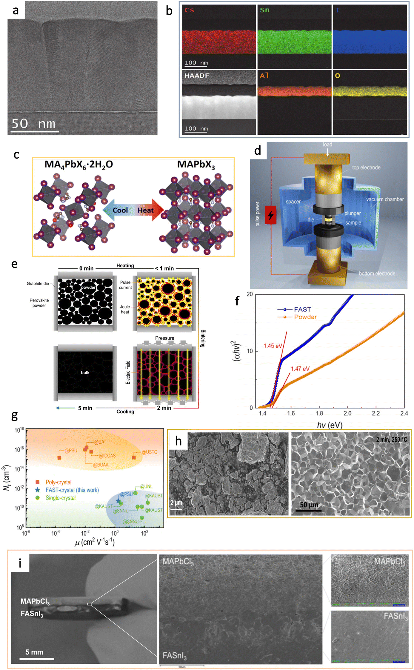 | ||
| Fig. 3 (a) Cross-section bright-field TEM image of a PLD-grown black γ-CsSnI3 film on Si. Reproduced with permission.38 Copyright 2020, Wiley-VCH. (b) High-angle annular dark-field (HAADF) image and EDX mapping of the constituent elements of CsSnI3 and the Al2O3 capping layer. EDX confirms uniform distribution of Cs, Sn, and I along the thickness of the layer and conformal coating of the Al2O3 capping layer. Reproduced with permission.38 Copyright 2020, Wiley-VCH. (c) Schematic of the reversible transformation between MA4PbX6·2H2O and MAPbX3. Reproduced with permission.42 Copyright 2021, American Chemical Society. (d) Schematic of the FAST equipment. Reproduced with permission.4 Copyright 2022, Springer Nature. (e) Processing diagram showing the solid densification of halide perovskites in a graphite die. Reproduced with permission.4 Copyright 2022, Springer Nature. (f) Tauc plot for powder and FAST-MAPbI3. Reproduced with permission.4 Copyright 2022, Springer Nature. (g) Comparison of trap density and mobility between FAST-MAPbI3 and state-of-the-art solution-processed thin film and single crystal of MAPbI3. The orange square, blue star, and green circle represent the poly-crystal, the FAST-crystal, and the single crystal, respectively. Reproduced with permission.4 Copyright 2022, Springer Nature. (h) SEM images of the ball-milled MAPbI3 (left) and FAST-MAPbI3 (right). Reproduced with permission.4 Copyright 2022, Springer Nature. (i) Photo of the bilayer heterojunction of MAPbCl3 and FASnI3, magnified cross-sectional SEM at the heterointerface, showing an intimate interface between the two perovskites. Reproduced with permission.4 Copyright 2022, Springer Nature. | ||
Solvent-free mechanochemical synthesis can also be used to prepare degradation or by-products of 3D perovskite counterparts, which can be converted to perovskite by certain treatments. In 2021, Palazon et al. synthesized 0D MA4Pb(Br1−xIx)6·2H2O powders by ball milling, and demonstrated MA4PbI6·2H2O reversible transformation to a 3D perovskite analog (MAPbI3) by controlled (de)hydration under thermal annealing and simple cooling in humid air conditions (Fig. 3c).42 Based on the conventional mechanochemical (ball milling) method, our group recently reported a new electrical and mechanical field-assisted sintering technique (EM-FAST, FAST for simplicity) for the preparation of high-quality perovskite.4 The whole process was operated in an airtight chamber consisting of a mechanical loading system with a high-power electrical circuit in a controlled atmosphere (Fig. 3d). Perovskite powder (by ball milling) was fixed in the die which was quickly heated to a high temperature by a high pulse current (1–10 kA). Meanwhile, the opposite static mechanical stress was applied simultaneously up and down to compress the sample. Through rapid heating and compressing, the powder sample could transform into a solid bulk crystal (Fig. 3e). Certain properties of FAST-MAPbI3 are similar to single crystals. According to the Tauc plot (Fig. 3f), the optical bandgap of FAST-MAPbI3 was calculated to be 1.45 eV, which is closer to the optical bandgap of a single crystal (1.51 eV) than to the typical thin film optical bandgap (1.6 eV). Using single carrier space charge limited current (SCLC) theory, the calculated trap density and hole mobility of FAST-MAPbI3 are 5.4 × 1010 cm−3 and 1.7 cm2 V−1 s−1, respectively. These values of FAST-MAPbI3 are located in a region closer to the single crystals rather than typical polycrystalline films in the trap density–mobility plot (Fig. 3g), and the trap density is significantly lower than that of solution-processed MAPbI3. Trap density and hole mobility can be expressed by the equations:
 | (5) |
 | (6) |
 | (7) |
Vapor vacuum deposition methods
In addition to mechanochemical synthesis methods, vapor-based synthesis methods also play an important role in the solvent-free synthesis of the perovskite films, and have been continuously developed and improved in the past decade. The vapor-deposition method was first applied to prepare layered perovskite crystals in 1997. Tsutsui et al. demonstrated the early possibility of preparing layered and cubic perovskites by dual-source vapor deposition of lead iodide and organic ammonium iodide.43 Later, many researchers noticed that the excellent properties of perovskites allowed them to use alternative materials for solar cells. The power conversion efficiency (PCE) of the perovskite solar cells (PSCs) has improved from 15.4% in the first work about vapor-deposited PSCs to 24.24% in the latest research results in 2022.44,45 Although the PCE of the vapor-processed PSCs is slightly inferior to that of the solution method-based devices, the precise regulation of the film's composition, crystallinity, thickness, uniformity, and other parameters indicate that the vapor-processed method shows great potential in massive and large-area fabrication of perovskite thin films in the future.In general, the core of the vapor-based method is to obtain the gas phase state of the required components by heating evaporation or sublimation, and then precisely controlling the process of vapor deposition onto the substrate in a high or low vacuum chamber. In view of the different deposition sequences of various precursor components in the vapor-based methods, researchers have developed two deposition techniques: co-evaporation deposition and sequential evaporation deposition. Here, we list the representative cutting-edge progresses in these scenarios with regard to high-quality samples.
The co-evaporation method has demonstrated good controllability of the performance of the perovskite, whereby the optimization of perovskite performance can be achieved by artificially changing the content of certain components within the film. It has been proved that both the different halide elements (Cl−, Br− and I−) and the different cations (Cs+, MA+, and FA+) showed impacts on the comprehensive properties of the perovskite films. Although the co-evaporation method has shown outstanding advantages in the preparation of perovskite films, the controllability and real-time monitoring in the process of co-evaporation are still a challenge, especially for the control of the evaporation rate of multiple precursors and the monitoring of film thickness. In a typical co-evaporation method, several quartz-crystal-monitors (QCMs) are fixed near the crucibles with precursors or substrate to simultaneously monitor the deposition status of multiple precursors and the thickness of the layers. Different precursors may interfere with each other's QCM readings during evaporation, especially when precursors with similar properties are being evaporated simultaneously. Thus, the monitored evaporation rates are not highly reliable, and film thickness and deposition rates are often over- or under-estimated, ultimately affecting film quality, resulting in reduced device performance.46,47 To solve this problem, layer-by-layer sequential vapor deposition is an alternative technique that can obtain high-quality and homogeneous perovskite films for the fabrication of high-performance devices, while avoiding the risk of cross-contamination of lead halide and organic ammonium salts.45
Organic cation perovskite
In 2013, Snaith et al. reported the deposition of CH3NH3PbI3−xClx film with a dual-source co-evaporation technique.44 The perovskite absorbers were deposited simultaneously through dual-source evaporation from lead chloride (PbCl2) and methylammonium iodide (CH3NH3I) onto the TiO2-compact-layer-coated fluorine-doped-tin-oxide (FTO) substrates (Fig. 4a). Two sensors directly above the evaporation source monitored the evaporation rates of the two materials, as the film quality was very sensitive to the relative ratio of CH3NH3I to PbCl2 and the overall deposited thickness. The deposited films were extremely uniform and appeared to be crystalline in length scales of hundreds of nanometers, whereas the solution-processed films exhibited numerous deep voids and only partially coated the substrate (Fig. 4c). Similarly, the cross-sectional image of the vapor-deposited perovskite (Fig. 4d) showed good flatness with an average thickness of ∼330 nm, while the solution-processed perovskite film showed an undulating nature with thickness varying from 50 to 410 nm. This remarkable difference in film quality would be more remarkable in large-scale fabrication. In 2014, Lin et al. prepared MAPbI3 perovskite using a layer-by-layer vacuum sublimation technique under 100 °C.46 It was demonstrated that PbI2 was in situ converted to perovskite during the sequential deposition process. Li et al. reported a layer-by-layer vacuum deposition technique for perovskite.48 By alternating the PbCl2 and MAI precursor layers, they obtained MAPbI3−xClx devices with an average PCE of 16.03%. Compared with co-evaporation methods, the layer-by-layer vapor deposition technique simplifies the deposition rates and thin film composition. Bolink et al. prepared MAPb(BrxI1−x)3 perovskites with three-source co-sublimation of MAI, lead iodide (PbI2), and lead bromide (PbBr2) in 2018 (Fig. 4b).49 The evaporation rates of PbI2 and PbBr2 were controlled by adjusting the temperatures of the crucibles. The deposition rate of PbBr2 with respect to PbI2 was increased while the rate of MAI remained constant, and the prepared champion devices based on MAPb(Br0.2I0.8)3 and MAPb(Br0.5I0.5)3 showed different photovoltaic properties (open-circuit voltages (Voc) of 1.080 V, 1.128 V; fill factors (FF) of 80.7%, 79.3%; PCEs of 14.7%, 5.5%, respectively).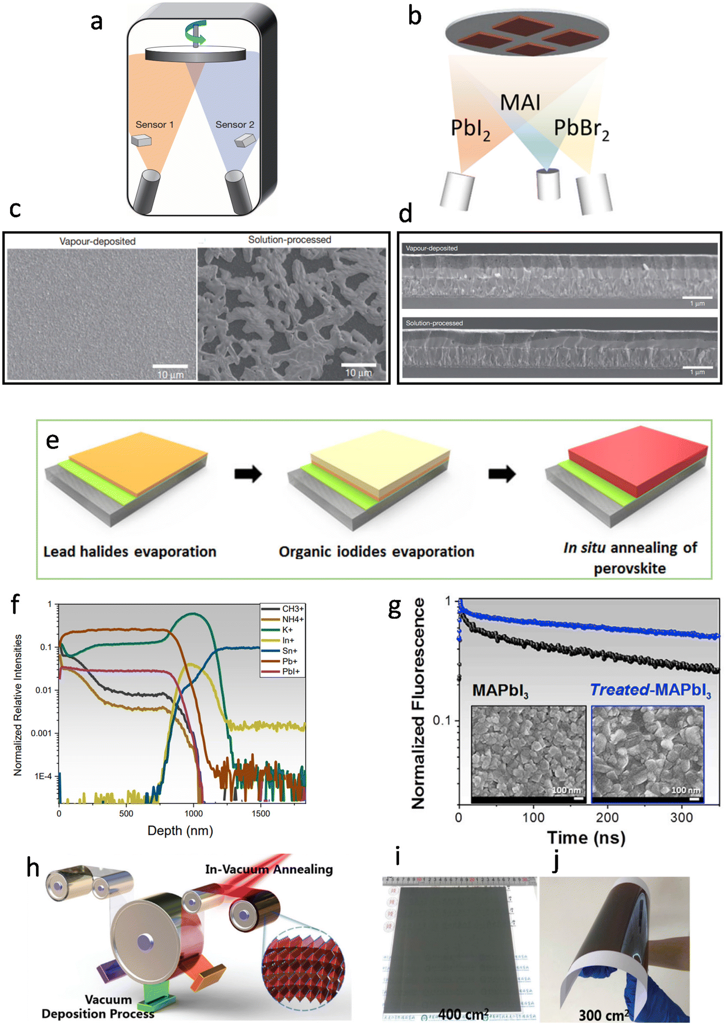 | ||
| Fig. 4 (a) Schematic of the dual-source thermal evaporation system for depositing the perovskite absorbers, the left source was methylammonium iodide, and the right source was PbCl2. Reproduced with permission.44 Copyright 2013, Springer Nature. (b) Schematic of three-source co-evaporation of the perovskite films. Reproduced with permission.49 Copyright 2017, American Chemical Society. (c) SEM top views of a vapor-deposited perovskite film and a solution-processed perovskite film. Reproduced with permission.44 Copyright 2013, Springer Nature. (d) Cross-sectional SEM images under lower magnification of completed solar cells constructed from a vapor-deposited perovskite film and a solution-processed perovskite film. Reproduced with permission.44 Copyright 2013, Springer Nature. (e) Schematic illustration of the fabrication procedures of an all-vacuum-deposited perovskite film. Reproduced with permission.50 Copyright 2019, Wiley-VCH. (f) The depth profile for the positive ions (CH3+, NH4+, K+, In+, Sn+, Pb+, PbI+) on a treated-MAPbI3 film deposited on PCBM/SnO2/FTO glass substrate. Reproduced with permission.54 Copyright 2020, Elsevier Inc. (g) TRPL decays and top-view SEM images of pristine MAPbI3 (black line) and treated-MAPbI3 (blue line). Reproduced with permission.54 Copyright 2020, Elsevier Inc. (h) Schematic of multisource vacuum deposition with an in-vacuum annealing process for large-area perovskite films; photographs of FA-based perovskite films deposited on (i) glass and (j) flexible polyethylene terephthalate (PET) substrates. Reproduced with permission.56 Copyright 2021, Royal Society of Chemistry. | ||
In 2019, Fan et al. proposed a special sequential vapor deposition method to deposit uniform mixed-cation mixed-halide (MAyFA1−yPbIxBr3−x) perovskite films. The devices fabricated based on this strategy showed a PCE of 15.14% (Fig. 4e).50 Moreover, the implementation of sputtered SnO2 films as the electron transport layer (ETL) was firstly demonstrated. Before the evaporation, PbI2 and PbBr2 with an optimized ratio were mixed in one crucible, and as their boiling points were quite close, they could both be fully evaporated. Subsequently, the MA and FA could also be fully evaporated at a very similar rate. In each step, only one crucible was heated to vaporize the precursor, so only one QCM was used to detect the evaporation rate, avoiding the usage of multiple sources.
The ratio between precursors is an important parameter to tune the final crystal quality. For example, Johnston et al. quantified the influence of excess PbI2 on the vapor deposition process of high-quality MAPbI3 formation.51 Excess PbI2 could not only make the bulk or grain boundaries directly passivated, but it also promotes the growth of perovskite crystals with better carrier properties. In addition, excess PbI2 greatly enhanced the absorption of MAI. When only MAI was deposited, there was no MAI on the FTO or glass substrates. The quartz microbalance thickness monitors also proved that the absorption of MAI near the PbI2 substrate was obviously higher than that in PbI2-free areas. Notably, the residual PbI2 made contributions to the photocurrent improvement while the unreacted PbI2 might lead to the photoinstability of the perovskite films.52,53 These carrier transport features can be further tuned through surface treatment.
Bruno et al. implemented a new surface treatment strategy to improve charge carrier transport at the grain boundaries within the MAPbI3 film.54 It has been demonstrated that a few intrinsic point defects such as Pb–I anti-site defects (PbI3−) could be found after the evaporation of organic cations and halides.55 To minimize the adverse effects on film quality, they introduced K+ from potassium acetate (KAc) to improve grain boundary conductivity through the immobilization of uncoordinated species. K+ could permeate deeply and homogeneously in thick MAPbI3 films, and the conductivity of the films was improved with deeper penetration (Fig. 4f). The combination of MAI and KAc could also improve the film morphology, which was reflected by reduced pinholes and increased particle size of the perovskite crystals (Fig. 4g). In 2021, Liu et al. prepared large-area perovskite films on rigid (400 cm2, Fig. 4i) and flexible (300 cm2, Fig. 4j) substrates by sequential vapor deposition (Fig. 4h).56
Due to the easiness in the preparation of large-area perovskite films with the vapor method, MAPbI3 was the preferred perovskite material for research in the beginning. However, the intrinsic instability of MA+ to thermal stress and the ambient air conditions limit the reliability of MAPbI3-based devices under high-temperature conditions and in other complex environments.57–59 Formamidinium iodide (FAI)-based perovskite absorber layers with superior thermal stability have become the preferred choice for the fabrication of single-junction PSCs, and PCEs over 25% were achieved for FA-based PSCs by the solution-based deposition method.60–65 Researchers paid more attention to perovskites containing Cs+ and FA+ for their superior long-term stability and high PCEs.66–71 Additionally, the incorporation of CsI in perovskites resulted in high quality perovskite films without pinholes and improved the stability of flexible PSCs (after 400 bends at a radius of 4 mm, the PCE remained ∼94% of the initial value).72
Organic–inorganic cation perovskite
In 2017, Liu et al. reported the fabrication of pin-hole-free cesium substituted perovskite films by a vacuum co-evaporation method, and the MA0.77Cs0.23PbI3 PSC exhibited a PCE of 20.13%, increased by ∼27% as compared to the pristine MAPbI3 based devices.73 To study the effect of Cs substitution on the crystallization of the MAPbI3 film, X-ray diffraction (XRD) was utilized to characterize the perovskite films with different Cs amounts (0, 0.11, 0.17, 0.23 and 0.34). In the magnified version of the (110) diffraction peak of MA1−xCsxPbI3, the 2θ monotonously moves from 14.14° to 14.36° with Cs content increasing from 0 to 0.34 (Fig. 5a), which proved that Cs cations could be integrated into the MAPbI3 lattice. Moreover, with the increase in Cs cation content, the bandgap of MA1−xCsxPbI3 was enlarged linearly (Fig. 5b) and the absorption peak shifted to shorter wavelength (Fig. 5c), demonstrating that the band gap of MA1−xCsxPbI3 can be fine-tuned by the Cs substitution. The prepared Cs-substituted PSCs show higher stability than typical MAPbI3-based devices with the PCE decreased by only 4.37% of the initial efficiency after the PSCs were stored in the dark for one year. The high stability of the Cs-substituted PSCs could be attributed to the high purity of the crystalline phase, low trap-state density, reduced lattice constant and relaxed strain after the incorporation of Cs.48,74 | ||
| Fig. 5 (a) XRD zoomed in on (110) diffraction peaks of perovskite based on various Cs contents. Reproduced with permission.73 Copyright 2017, Royal Society of Chemistry. (b) The linear relationship of the band gap of perovskite with Cs content. Reproduced with permission.73 Copyright 2017, Royal Society of Chemistry. (c) The band gap of MAPbI3 with different Cs content. Reproduced with permission.73 Copyright 2017, Royal Society of Chemistry. (d) Photograph of the employed evaporation chamber. Reproduced with permission.75 Copyright 2018, Wiley-VCH. (e) Cross-section SEM image of the CsPbBr3–GaN heterojunction. The cross-section of the CsPbBr3 microplatelet single-crystals (MPC) is uniform rectangular. Scale bar: 2 μm. Reproduced with permission.79 Copyright 2019, American Chemical Society. (f) Polarized optical microscopy (OM) image for a single grain. The inset is the photograph of CVD grown CsPbBr3 film with mm-scale grains. (g) Schematic illustration of CVD setup: a two-zone furnace, where the precursor is placed at zone-I, and substrate positions (marked as A, B, and C) are placed in zone-II. Reproduced with permission.80 Copyright 2021, Wiley-VCH. (h) The tube-in-tube setup for the vapor phase epitaxial growth of the CsPbBr3 nanoplates and single crystal thin films on STO substrates under higher temperature (450 °C). Reproduced with permission.81 Copyright 2017, American Chemical Society. (i) Top-view SEM images of PbCl2-alloy-mediated film and reference film. Reproduced with permission.45 Copyright 2022, Science. (j) Top view SEM images of the perovskite thin films fabricated at substrate temperatures of 65 °C, 75 °C, and 85 °C. Reproduced with permission.46 Copyright 2014, Wiley-VCH. | ||
In 2018, Bolink et al. first reported the preparation of multications/anions perovskite compounds using a multiple sources (3 or 4) thermal vacuum deposition method (Fig. 5d).75 However, the uniformity of the films was poorer than that of the samples obtained by simple vacuum vapor deposition methods, indicating that more research was needed to control the morphological homogeneity in the multi-source co-deposition method. Similar results about the effect of excess PbI2 were observed in FA based perovskites by Stranks et al. in 2020.76 In the fabrication of FA0.7Cs0.3Pb(I0.9Br0.1)3 films, excess PbI2 enhanced the film stability and photoelectric properties, yielding longer carrier lifetimes and high photoluminescence quantum efficiency (PLQE). The resultant PSC showed a stable PCE of 18.2% which was the highest performance for the vapor-deposited MA-free system. Li et al. obtained a high-quality Cs0.24FA0.76PbI3−xBrx film with 4 nm SrI2 to accelerate the conversion rate of PbI2 to perovskite, and the film showed large grain sizes, and low trap-state density.77 This indicates that a moderate amount of SrI2 could promote the conversion of PbI2 to perovskite and achieve a champion PCE of 17.66% with a high FF up to 0.79. Later in 2021, Bolink et al. showed the preparation of FA1−nCsnPb(I1−xBrx)3 samples by four-source evaporation under room temperature.78 The bandgaps of the perovskites were tuned between 1.7 eV and 1.8 eV by controlling the amount of bromide and cesium, and the champion PSC exhibited a PCE of 16.8% and retained 90% of its initial efficiency after 2 weeks of continuous operation.
Inorganic cation perovskite
In 2017, Chen et al. reported that they had successfully grown controllable and large-area continuous single-crystalline CsPbBr3 thin films on SrTiO3(100) substrates by a facile vapor-phase epitaxy growth, as well as directionally aligned CsPbBr3 nanosheet arrays (Fig. 5h).81 The resulting single-crystalline CsPbBr3 exhibits excellent crystal quality and optoelectronic properties, such as slow carrier recombination rates, low surface recombination velocities, and low bulk defect densities. Later in 2019, large-area and high-quality CsPbBr3 single crystals were grown on GaN/sapphire substrates by the CVD method.79 The CsPbBr3-GaN formed a type II semiconductor heterojunction, indicating a great opportunity for developing application-level wide-bandgap perovskite micro/nano optoelectronic and photonic devices (Fig. 5e). In 2021, Zhou et al. found that the key to large-grain CsPbBr3 crystals was to control the crystal growth rate.80 They demonstrated the preparation of CsPbBr3 crystals with a grain size of up to 3.1 mm by controlling the growth rate, which was affected by the gas flow rate and deposition location (Fig. 5f & g). In 2022, Yi et al. developed a Cl-alloy-mediated sequential vacuum deposition method for fabricating high-efficiency PSCs with a maximum PCE of 24.42%.45 They demonstrated that the introduction of a moderate amount of Cl in Cs0.05PbI2.05−xClx could accelerate the solid-state diffusion of organic ammonium salt into the lead iodide lattice. Besides, Cl facilitated the crystallization of perovskite and improved the film homogeneity by the reduction of the grain boundaries.82 It can be seen in Fig. 5i that the PbCl2-alloy-mediated film shows a larger grain size under the same annealing time as compared to the plain samples, which indicated fewer defects within the prepared film, resulting in the reduction of the Shockley–Read–Hall (SRH) recombination. More importantly, the phase conversion from α- to δ-phase is one of the main drawbacks of FAPbI3 perovskites and the doping of Cl promotes the transition from the δ-phase to the α-phase and reduces the amount of δ-phase within the perovskite film.83–85It is important to monitor and control the evaporation rate of the precursor in the vapor phase method, while the relevant parameters of the deposited substrate, such as crystallinity, orientation, lattice parameter and morphological properties, also have a significant impact on the performance of the film.86–88 In 2014, Lin et al. observed different crystalline morphologies in perovskite films deposited on substrates with different temperatures.46 When the substrate was heated to 65 °C, only the upper part of PbI2 reacted with MAI to form the perovskite layer, while the bottom part of the PbI2 still remained unchanged. As the temperature gradually increased to 75 °C and 85 °C, the crystal structures were first observed to be fused together and have fuzzy domain boundaries, and the domains reappeared vividly at 85 °C but with a much smaller domain size of about 200 nm (Fig. 5j). Moreover, when the film was sublimated at 85 °C, the crystallization was not as pure as the film at a substrate temperature of 75 °C, probably due to the violent reaction of MAI and PbCl2 at 85 °C. Qi et al. investigated the effect of substrate temperature variation on the adhesion of MAI on the substrate, and the adhesion coefficient of MAI gradually decreased with the increasing of substrate temperature, resulting in the best device performance with Voc of 1.010 V, Jsc of 12.85 mA−2, FF of 66.60%, and overall PCE of 8.64%.89 Meanwhile, the type and chemical properties of the substrate not only affect the growth of the perovskite but also directly impact the energetics of the interface, which determines the rate of extraction and recombination of photogenerated charges in solar cells.90 For instance, the UV photoelectron spectroscopy (UPS) spectra of MAPbI3 were obtained after the increasing of the thickness of MAPbI3 layer-by-layer on different substrates, such as polyethyleneimine (PEIE) and poly(3,4-ethylenedioxythiophene)polystyrene sulfonate (PEDOT:PSS). The results showed that the material characteristics of MAPbI3 could be detected on (PEDOT:PSS) substrates after only 3 nm thickness. In contrast, the formation of perovskite on metal oxide substrates like MoO3 or indium tin oxide (ITO) was only observed when the deposition thickness was 10 nm or 30 nm, respectively.91,92
Outlook and challenges
Benefits of solvent-free methods
 | ||
| Fig. 6 (a) Dark, forward, and backward J–V curves of treated-MAPbI3 PSCs with active areas ranging from 0.16 to 4 cm2. Reproduced with permission.54 Copyright 2020, Elsevier Inc. (b) The J–V curves of a device with >2 cm2 Au electrode measured with different square mask areas. Reproduced with permission.93 Copyright 2019, Elsevier Inc. (c) Evolution of the power conversion efficiencies of FAPbI3 PSCs based on the precursor solution aged for different times. Reproduced with permission.99 Copyright 2022, Wiley-VCH. | ||
The defect tolerance of metal halide perovskites refers to the predominance of shallow-level defects, which do not act as strong non-radiative recombination centers.94 This is considered a unique characteristic of metal halide perovskites and a key reason for their high photovoltaic conversion efficiency, especially in small-area devices. However, non-radiative recombination centers and deep-level defects produced by factors such as point defects, grain boundaries, surfaces, and interfaces still reduce the PCE of PSCs, remarkably for the large area devices. As mentioned above, with increasing device area, solution processing exhibits inhomogeneity in film formation from the center to the edge, resulting in a higher number of defects and significantly lower film quality compared to vacuum deposition.32
In the solution processed method, the vapor pressure of the solvent is determined by temperature and humidity, and the nucleation and growth of perovskite grains are strongly affected by solvent evaporation.95 To obtain reproducible perovskite films, it is necessary to control the temperature and humidity to be consistent throughout the experimental process. In addition, it has been proved that progressive chemical reactions occur in precursor solutions stored under an inert gas atmosphere, indicating different reaction components may participate in the preparation of perovskite films while using the same precursor solution at different times.96–98 This may lead to significant deviations in PSC performance (Fig. 6c), which results in non-reproducibility of perovskite film quality and device performance between batches and among different laboratories.99
In contrast, the vacuum deposition method is solvent-free and performed under high vacuum (≈10−6 Torr), where atmospheric gas molecules are rare. This avoids the impact of some organic solvents in the solution method on the absorption of moisture in the environment, which may affect the quality of perovskite films. In large-scale production, after optimizing the parameters of the equipment, fixed process parameters can be used for deposition to obtain perovskite films with good reproducibility. Organic light-emitting diode (OLED) devices based on thermal evaporation technology have been successfully launched on the market. Recently, a 97-inch OLED display has been released, which supports the compatibility of thermal evaporation technology with large-area film and device fabrication.99
In summary, the vapor-phase methods demonstrate the potential for future preparation of large-area, high-quality, and reproducible perovskite films in multiple batches.
 | ||
| Scheme 1 Retrosynthetic approach for the synthesis of inorganic perovskite type halides using CsX and PbX2 as solid precursors. | ||
High-energy ball milling can introduce energy between the powder of different reactants, thereby promoting the reaction. The degree of reaction completion and chemical stoichiometry can be controlled by adjusting the ball milling rotation speed and time. Pal et al. demonstrated post-synthetic solid-state transformations of CsPbBr3 to CsPb2Br5, and Cs4PbBr6 (Scheme 2),1 which indicated that reaction time and degree of reaction have a significant effect on the composition and structure of the reaction products. Moreover, other factors also need to be taken into consideration, such as the high temperature required for solvent-free synthesis methods, as well as knowledge of the melting points and decomposition temperatures of the precursors and different perovskite materials.40
 | ||
| Scheme 2 Post-synthetic solid-state transformations of CsPbBr3 to CsPb2Br5 and Cs4PbBr6. | ||
Regarding the vapor deposition method, the evaporation and deposition rates of the different precursors in the vacuum chamber largely reflect the stoichiometric ratios of different elements in perovskite. In the evaporation process for organic perovskite, the vapor pressure and diffusivity of low-molecular-weight organic halides can cause unnecessary deposition on the chamber wall, which may cause additional deposition or introduction of impurities in the next vapor deposition cycle; thus, an unwanted stoichiometric ratio of perovskite can be present.99 Recently, perovskite precursors with large molecular weight (FAI) and high sublimation temperature (CsX, X = I, Br, Cl) have been discussed to avoid this problem. Additionally, the state-of-the-art evaporators with a cooling system for the inner chamber wall can prevent redeposition of organic halides.
Quartz crystal microbalances (QCM) are widely used for detecting evaporation rates of corresponding precursors. It was reported that adjusting the position of the QCM and using shielding around the QCM can prevent cross-read on sensors, thereby improving the accuracy of the measured evaporation rates of the precursors.100 Bolink et al. conducted a comprehensive study of the vacuum deposition of MAPBI3 perovskite and established a growth kinetic model, which could control the stoichiometry of MAPbI3 during the vacuum co-deposition process. To accurately control the stoichiometry of perovskite deposited by the gas-phase method, it is necessary to establish growth kinetic models that are applicable to different materials. Roß et al. revealed that the stoichiometry of the deposited film was influenced by the substrate temperature which significantly affected the adhesion of MAI. High substrate temperature prevented the adhesion of MAI and may accelerate the thermal decomposition of MAI (Fig. 7).101 Thus, a suitable substrate temperature should be set for the vacuum deposition of MAI based perovskites.
 | ||
| Fig. 7 Box plot of power conversion efficiency extracted from J–V scans (reverse and forward) measured under simulated AM 1.5G illumination for solar cells prepared at different substrate temperatures and MAI rates on (a) PTAA and (b) MeO-2PACz. (c) Normalized XRD patterns of co-evaporated films on PTAA deposited with different substrate temperatures. Reproduced with permission.101 Copyright 2020, American Chemical Society. | ||
Existing challenges
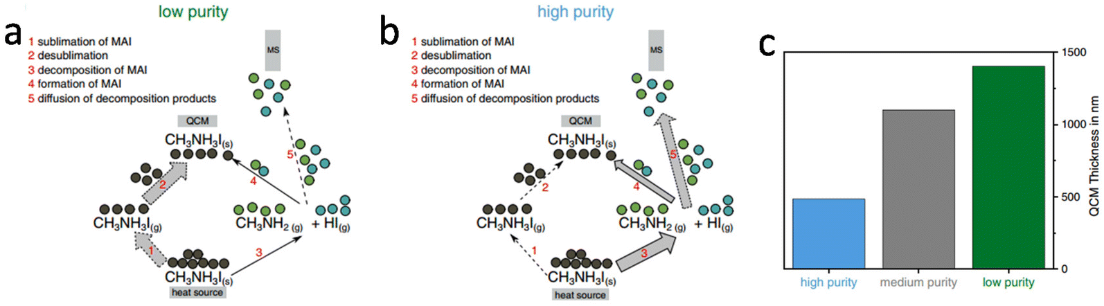 | ||
| Fig. 8 Schematic of sublimation and decomposition processes. For low purity MAI (a), the main path (thick arrows) is the sublimation and desublimation. For high purity MAI (b), the main path is the decomposition into methylamine and hydrogen iodide. (c) Comparison of the peak areas extracted for each material. Reproduced with permission.103 Copyright 2022, Wiley-VCH. | ||
Promising potential
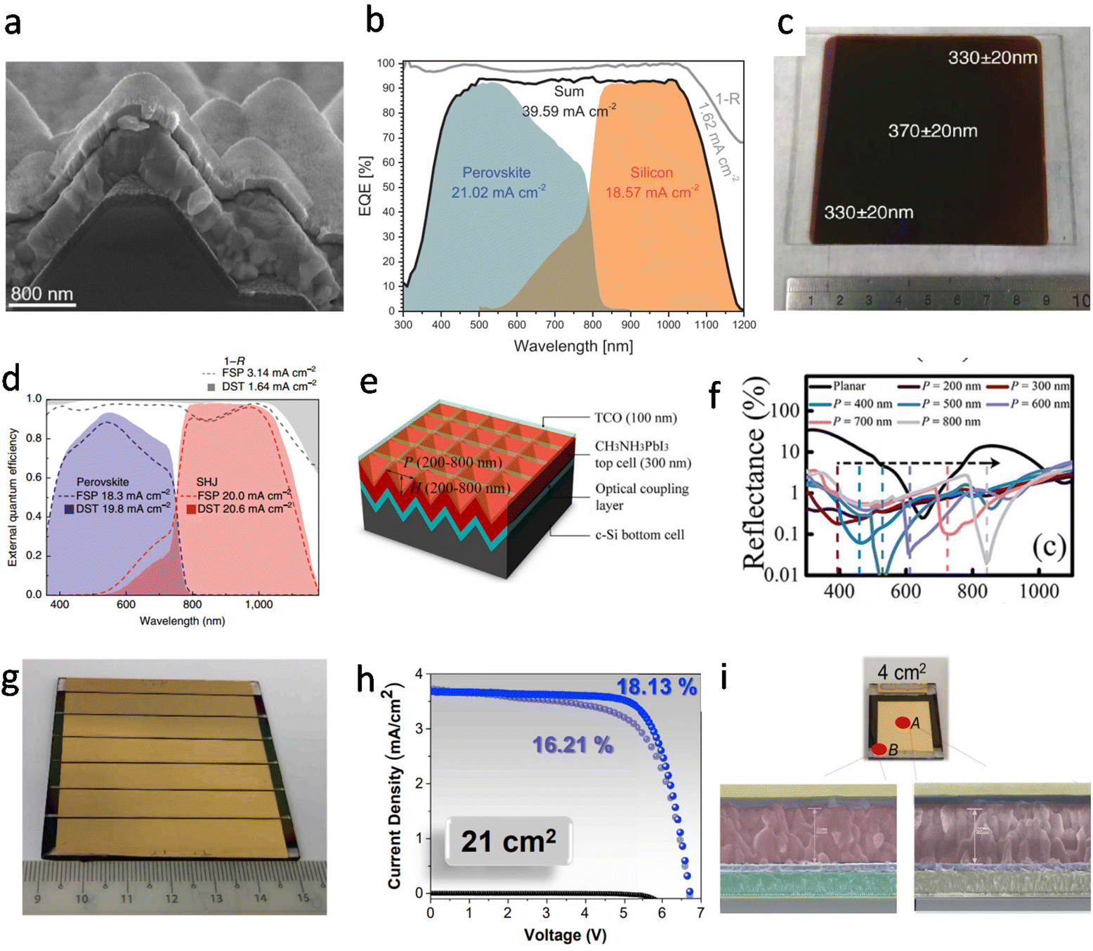 | ||
| Fig. 9 (a) Cross-sectional SEM image of textured silicon bottom cells covered with MA0.5FA0.63PbI3.13, capped with 18 nm of C60 and after the 20 nm SnO2 ALD deposition. Reproduced with permission.110 Copyright 2021, Wiley-VCH. (b) EQE and reflection spectra (denoted as 1 − R) including the integrated current densities of the two sub cells, the sum and reflection. Reproduced with permission.110 Copyright 2021, Wiley-VCH. (c) Photograph of 8 cm × 8 cm thin film of FAPbI3 deposited on a glass substrate. The image shows the substrate after thermal annealing at 170 °C for 1 min. The results of thickness measurements at three positions are superimposed on the image, and a metal ruler with a centimeter scale is shown as a size reference. Reproduced with permission.116 Copyright 2017, American Chemical Society. (d) Improved optics with a fully textured architecture. EQE of perovskite/SHJ monolithic tandem cells with double-side-textured (DST) or front-side-polished (FSP) bottom cells, alongside corresponding total absorptance curves, 1 − R, where R is the reflectance of the device. These EQE and 1 − R spectra do not include losses due to the front-side metal grid. Reproduced with permission.113 Copyright 2018, Springer Nature. (e) Schematic of perovskite/c-Si tandem solar cells (TSC) with inverted nanopyramid structure. The parameters H and P denote the pyramid height and its period, respectively. (f) Reflectance of inverted nanopyramid perovskite/c-Si TSC. Reproduced with permission.115 Copyright 2015, Springer Nature. (g) Image of a 21 cm2 active area perovskite solar module consisting of 6 series-connected sub-cells. Reproduced with permission.54 Copyright 2020, Elsevier Inc. (h) Treated-MAPbI3 perovskite solar module dark, forward, and backward J–V curves measured in air. Reproduced with permission.54 Copyright 2020, Elsevier Inc. (i) 4 cm2 PSC photograph and cross-sectional SEM images of point A and point B. Reproduced with permission.54 Copyright 2020, Elsevier Inc. | ||
Conclusion and perspectives
In conclusion, we have mainly summarized two solvent-free methods for the synthesis of various high-quality perovskites: mechanochemical synthesis and vapor deposition-based synthesis. These two methods can not only circumvent the shortcomings of the mainstream solution-based fabrication methods, such as solvent toxicity, high solvent cost, and poor film formation, but also provide new ideas for the fabrication of large-area perovskite films with excellent optoelectronic properties and greater possibility for mass production considering reproducibility, uniformity, energy–time input, and cleanness, which may pave the route towards real applications based on the halide perovskite materials.Although the above-mentioned solvent-free synthesis methods are constantly being developed and improved, and significant breakthroughs and achievements have been achieved, there are still problems to be solved and space for improvement. (i) Compared with the solution method, the solvent-free method reduces the toxicity of the solvent, but the involvement of the heavy metal lead in most perovskites still makes the experimental process toxic. While significant progress has been made in the field of Pb-free chalcogenide synthesis,116 the latest Pb-free PSCs are now available at a maximum of 14.81%. The development of lead-free perovskite with solvent-free synthesis methods would be a landmark solution. (ii) The tunable absorption band gap of perovskite makes it promising for the multi-junction applications. For example, recent studies have demonstrated the preparation of all-perovskite tandem solar cells with record PCE.117 Briefly, Chiang et al. fabricated all-perovskite tandem solar cells using fully-evaporated methods (employing four evaporation sources), which demonstrated an open circuit voltage of 2.06 V and a power conversion efficiency (PCE) of 24.1%.76 Recognizing this achievement, additional literature on the synthesis of all-perovskite tandem solar cells using vapor-based methods, as opposed to solution-based approaches, also include the following examples. In 2018, Ávila et al. demonstrated the preparation of CH3NH3PbI3–CH3NH3PbI3 tandem solar cells with PCEs exceeding 18%.117 The devices exhibited a remarkably high open-circuit voltage of 2.3 V, confirming the feasibility of the vapor deposition approach for fabricating high-performance tandem PSCs. In addition to the all-vapor-phase deposition method, researchers have also employed combinations of gas-phase and solution-based approaches for all-perovskite tandem solar cells. Palmstrom et al. suggested that an orthogonal solvent system and a solvent-free approach could be utilized to deposit perovskite layers.118 Furthermore, Abdollahi Nejand et al. combined blade coating and vacuum-based deposition processes for the fabrication of all-perovskite tandem solar cells, successfully scaling up laboratory-sized devices from 0.1 cm2 to 12.25 cm2.119 These studies demonstrate the potential of vapor-based and hybrid deposition methods for the fabrication of high-performance all-perovskite tandem solar cells, further validating the relevance and importance of the focus on such approaches. Nevertheless, the perovskite layers in the vast majority of research on all-perovskite tandem solar cells are prepared by solution processing methods, where the presence of solvents has caused many adverse effects on the preparation of high-quality perovskite films as previously discussed. A less or solvent-free synthesis method is expected to optimize the preparation of multi-junction perovskite samples. While the main obstacle is the thickness control in these all-solid methods (for solar cell application the active layer thickness needs to be controlled at the sub-micrometer level to allow sufficient photocarrier drifting), where the mechanochemical methods are less likely compatible but vapor deposition methods hold potential. (iii) The main promise for the mechanochemical methods is the bulk sample application where thermoelectric devices typically require a thick electrode to ensure a sufficient temperature gradient for efficient thermal-electricity conversion, while high energy radiation detectors need a sufficiently large sample thickness to effectively absorb the radiation wave. Although there is a great endeavor being carried out in the direction of perovskite X-ray/gamma-ray detection, most prior reports utilized bulk single crystalline samples for the device. Future works may take advantage of the manufacturing flexibility of the mechanochemical methods to design new p–n junction samples, alloy samples, and multi-layer junction samples for these applications. Further promise can be the development of advanced manufacturing in conjunction with 3D printing techniques, mold printing, laser annealing, etc.
Conflicts of interest
There are no conflicts to declare.Acknowledgements
The authors from NPU acknowledge financial support from the Fundamental Research Funds for the Central Universities (D5000220072). The unfunded collaborative work of L. Z., A. N., B. P., and K. W. is supported by the International Institute of Biosensing (IIB), headquartered at Penn State University.References
- P. Pal, S. Saha, A. Banik, A. Sarkar and K. Biswas, All-Solid-State Mechanochemical Synthesis and Post-Synthetic Transformation of Inorganic Perovskite-type Halides, Chem. – Eur. J., 2018, 24, 1811–1815 CrossRef CAS PubMed.
- K. Wang, D. Yang, C. Wu, M. Sanghadasa and S. Priya, Recent progress in fundamental understanding of halide perovskite semiconductors, Prog. Mater. Sci., 2019, 106, 100580 CrossRef CAS.
- R. Vidal, J.-A. Alberola-Borràs, S. N. Habisreutinger, J.-L. Gimeno-Molina, D. T. Moore, T. H. Schloemer, I. Mora-Seró, J. J. Berry and J. M. Luther, Assessing health and environmental impacts of solvents for producing perovskite solar cells, Nat. Sustainability, 2021, 4, 277–285 CrossRef.
- L. Zheng, A. Nozariasbmarz, Y. Hou, J. Yoon, W. Li, Y. Zhang, H. Wu, D. Yang, T. Ye, M. Sanghadasa, K. Wang, B. Poudel, S. Priya and K. Wang, A universal all-solid synthesis for high throughput production of halide perovskite, Nat. Commun., 2022, 13, 7399 CrossRef CAS PubMed.
- G. Cao, Nanostructures & nanomaterials: synthesis, properties & applications, Imperial College Press, 2004 Search PubMed.
- B. Ding, Y. Li, S.-Y. Huang, Q.-Q. Chu, C.-X. Li, C.-J. Li and G.-J. Yang, Material nucleation/growth competition tuning towards highly reproducible planar perovskite solar cells with efficiency exceeding 20%, J. Mater. Chem. A, 2017, 5, 6840–6848 RSC.
- M. Haruta and B. Delmon, Preparation of homodisperse solids, J. Chim. Phys., 1986, 83, 859–868 CrossRef CAS.
- Y. Fu, F. Meng, M. B. Rowley, B. J. Thompson, M. J. Shearer, D. Ma, R. J. Hamers, J. C. Wright and S. Jin, Solution growth of single crystal methylammonium lead halide perovskite nanostructures for optoelectronic and photovoltaic applications, J. Am. Chem. Soc., 2015, 137, 5810–5818 CrossRef CAS PubMed.
- F. Huang, M. Li, P. Siffalovic, G. Cao and J. Tian, From scalable solution fabrication of perovskite films towards commercialization of solar cells, Energy Environ. Sci., 2019, 12, 518–549 RSC.
- S. J. Yoon, K. G. Stamplecoskie and P. V. Kamat, How lead halide complex chemistry dictates the composition of mixed halide perovskites, J. Phys. Chem. Lett., 2016, 7, 1368–1373 CrossRef CAS.
- B. A. Rosales, L. Men, S. D. Cady, M. P. Hanrahan, A. J. Rossini and J. Vela, Persistent dopants and phase segregation in organolead mixed-halide perovskites, Chem. Mater., 2016, 28, 6848–6859 CrossRef CAS.
- B. A. Rosales, M. P. Hanrahan, B. W. Boote, A. J. Rossini, E. A. Smith and J. Vela, Lead halide perovskites: Challenges and opportunities in advanced synthesis and spectroscopy, ACS Energy Lett., 2017, 2, 906–914 CrossRef CAS.
- L. Men, M. A. White, H. Andaraarachchi, B. A. Rosales and J. Vela, Synthetic development of low dimensional materials, Chem. Mater., 2017, 29, 168–175 CrossRef CAS.
- A. Karmakar, A. M. Askar, G. M. Bernard, V. V. Terskikh, M. Ha, S. Patel, K. Shankar and V. K. Michaelis, Mechanochemical synthesis of methylammonium lead mixed–halide perovskites: unraveling the solid-solution behavior using solid-state NMR, Chem. Mater., 2018, 30, 2309–2321 CrossRef CAS.
- M. P. Hanrahan, L. Men, B. A. Rosales, J. Vela and A. J. Rossini, Sensitivity-enhanced 207Pb solid-state NMR spectroscopy for the rapid, non-destructive characterization of organolead halide perovskites, Chem. Mater., 2018, 30, 7005–7015 CrossRef CAS.
- F. Brivio, C. Caetano and A. Walsh, Thermodynamic origin of photoinstability in the CH3NH3Pb(I1−xBrx)3 hybrid halide perovskite alloy, J. Phys. Chem. Lett., 2016, 7, 1083–1087 CrossRef CAS.
- A. M. Askar, A. Karmakar, G. M. Bernard, M. Ha, V. V. Terskikh, B. D. Wiltshire, S. Patel, J. Fleet, K. Shankar and V. K. Michaelis, Composition-tunable formamidinium lead mixed halide perovskites via solvent-free mechanochemical synthesis: decoding the Pb environments using solid-state NMR spectroscopy, J. Phys. Chem. Lett., 2018, 9, 2671–2677 CrossRef CAS PubMed.
- N. K. Noel, S. N. Habisreutinger, B. Wenger, M. T. Klug, M. T. Hörantner, M. B. Johnston, R. J. Nicholas, D. T. Moore and H. J. Snaith, A low viscosity, low boiling point, clean solvent system for the rapid crystallisation of highly specular perovskite films, Energy Environ. Sci., 2017, 10, 145–152 RSC.
- X. Cao, L. Zhi, Y. Jia, Y. Li, K. Zhao, X. Cui, L. Ci, D. Zhuang and J. Wei, A review of the role of solvents in formation of high-quality solution-processed perovskite films, ACS Appl. Mater. Interfaces, 2019, 11, 7639–7654 CrossRef CAS PubMed.
- J. Schlipf, P. Docampo, C. J. Schaffer, V. Körstgens, L. Bießmann, F. Hanusch, N. Giesbrecht, S. Bernstorff, T. Bein and P. Müller-Buschbaum, A closer look into two-step perovskite conversion with X-ray scattering, J. Phys. Chem. Lett., 2015, 6, 1265–1269 CrossRef CAS PubMed.
- R. Liu and K. J. M. Xu, Solvent engineering for perovskite solar cells: a review, Micro Nano Lett., 2020, 15, 349–353 CrossRef CAS.
- Y.-H. Seo, E.-C. Kim, S.-P. Cho, S.-S. Kim and S.-I. Na, High-performance planar perovskite solar cells: Influence of solvent upon performance, Appl. Mater. Today, 2017, 9, 598–604 CrossRef.
- Y. Li, Z. Zhao, F. Lin, X. Cao, X. Cui and J. Wei, In situ observation of crystallization of methylammonium lead iodide perovskite from microdroplets, Small, 2017, 13, 1604125 CrossRef.
- B. Cai, W.-H. Zhang and J. Qiu, Solvent engineering of spin-coating solutions for planar-structured high-efficiency perovskite solar cells, Chin. J. Catal., 2015, 36, 1183–1190 CrossRef CAS.
- N. Ahn, D.-Y. Son, I.-H. Jang, S. M. Kang, M. Choi and N.-G. Park, Highly reproducible perovskite solar cells with average efficiency of 18.3% and best efficiency of 19.7% fabricated via Lewis base adduct of lead(II) iodide, J. Am. Chem. Soc., 2015, 137, 8696–8699 CrossRef CAS PubMed.
- J. Zhao, Y. Deng, H. Wei, X. Zheng, Z. Yu, Y. Shao, J. E. Shield and J. Huang, Strained hybrid perovskite thin films and their impact on the intrinsic stability of perovskite solar cells, Sci. Adv., 2017, 3, 5616 CrossRef PubMed.
- C. N. R. Rao and K. Biswas, Soft Chemistry Routes, Essentials of Inorganic Materials Synthesis, 2015 Search PubMed.
- H. Zhou, Q. Chen, G. Li, S. Luo, T.-B. Song, H.-S. Duan, Z. Hong, J. You, Y. Liu and Y. Yang, Interface engineering of highly efficient perovskite solar cells, Science, 2014, 345, 542–546 CrossRef CAS.
- R. Karlicek, C.-C. Sun, G. Zissis and R. Ma, Handbook of advanced lighting technology, Springer, 2017 Search PubMed.
- X. Cao, L. Zhi, Y. Li, F. Fang, X. Cui, L. Ci, K. Ding and J. Wei, Fabrication of perovskite films with large columnar grains via solvent-mediated Ostwald ripening for efficient inverted perovskite solar cells, ACS Appl. Energy Mater., 2018, 1, 868–875 CrossRef CAS.
- J.-H. Im, I.-H. Jang, N. Pellet, M. Grätzel and N.-G. Park, Growth of CH3NH3PbI3 cuboids with controlled size for high-efficiency perovskite solar cells, Nat. Nanotechnol., 2014, 9, 927–932 CrossRef CAS PubMed.
- J. H. Heo, F. Zhang, C. Xiao, S. J. Heo, J. K. Park, J. J. Berry, K. Zhu and S. H. Im, Efficient and stable graded CsPbI3−xBrx perovskite solar cells and submodules by orthogonal processable spray coating, Joule, 2021, 5, 481–494 CrossRef CAS.
- X. Jia, C. Zuo, S. Tao, K. Sun, Y. Zhao, S. Yang, M. Cheng, M. Wang, Y. Yuan and J. Yang, CsPb(IxBr1−x)3 solar cells, Sci. Bull. Fac. Agric., Kyushu Univ., 2019, 64, 1532–1539 CAS.
- Y. Wang, T. Zhang, M. Kan, Y. Li, T. Wang and Y. Zhao, Efficient α-CsPbI3 photovoltaics with surface terminated organic cations, Joule, 2018, 2, 2065–2075 CrossRef CAS.
- M. Tai, Y. Zhou, X. Yin, J. Han, Q. Zhang, Y. Zhou and H. Lin, In situ formation of a 2D/3D heterostructure for efficient and stable CsPbI2 Br solar cells, J. Mater. Chem. A, 2019, 7, 22675–22682 RSC.
- L. Protesescu, S. Yakunin, O. Nazarenko, D. N. Dirin and M. V. Kovalenko, Low-cost synthesis of highly luminescent colloidal lead halide perovskite nanocrystals by wet ball milling, ACS Appl. Nano Mater., 2018, 1, 1300–1308 CrossRef CAS PubMed.
- P. Sebastia-Luna, J. Navarro-Alapont, M. Sessolo, F. Palazon and H. J. Bolink, Solvent-free synthesis and thin-film deposition of cesium copper halides with bright blue photoluminescence, Chem. Mater., 2019, 31, 10205–10210 CrossRef CAS.
- V. M. Kiyek, Y. A. Birkhölzer, Y. Smirnov, M. Ledinsky, Z. Remes, J. Momand, B. J. Kooi, G. Koster, G. Rijnders and M. Morales-Masis, Single-source, solvent-free, room temperature deposition of black γ-CsSnI3 films, Adv. Mater. Interfaces, 2020, 7, 2000162 CrossRef CAS.
- E. M. Gutman, Mechanochemistry of materials, Cambridge Int Science Publishing, 1998 Search PubMed.
- B. A. Rosales, L. Wei and J. Vela, Synthesis and mixing of complex halide perovskites by solvent-free solid-state methods, J. Solid State Chem., 2019, 271, 206–215 CrossRef CAS.
- O. Y. Posudievsky, N. V. Konoshchuk, A. G. Shkavro, V. L. Karbivskiy, V. G. Koshechko and V. D. Pokhodenko, Nanostructured Mechanochemically Prepared Hybrid Perovskites Based on PbI2 and Alkylammonium Halides for Optoelectronic Applications, ACS Appl. Nano Mater., 2018, 1, 4145–4155 CrossRef CAS.
- B. A. Huisman, F. Palazon and H. J. Bolink, Zero-dimensional hybrid organic–inorganic lead halides and their post-synthesis reversible transformation into three-dimensional perovskites, Inorg. Chem., 2021, 60, 5212–5216 CrossRef CAS PubMed.
- M. Era, T. Hattori, T. Taira and T. Tsutsui, Self-organized growth of PbI-based layered perovskite quantum well by dual-source vapor deposition, Chem. Mater., 1997, 9, 8–10 CrossRef CAS.
- M. Liu, M. B. Johnston and H. J. Snaith, Efficient planar heterojunction perovskite solar cells by vapour deposition, Nature, 2013, 501, 395–398 CrossRef CAS PubMed.
- H. Li, J. Zhou, L. Tan, M. Li, C. Jiang, S. Wang, X. Zhao, Y. Liu, Y. Zhang, Y. Ye, W. Tress and C. Yi, Sequential vacuum-evaporated perovskite solar cells with more than 24% efficiency, Sci. Adv., 2022, 8, 7422 CrossRef PubMed.
- C. W. Chen, H. W. Kang, S. Y. Hsiao, P. F. Yang, K. M. Chiang and H. W. Lin, Efficient and uniform planar-type perovskite solar cells by simple sequential vacuum deposition, Adv. Mater., 2014, 26, 6647–6652 CrossRef CAS PubMed.
- L. K. Ono, S. Wang, Y. Kato, S. R. Raga and Y. Qi, Fabrication of semi-transparent perovskite films with centimeter-scale superior uniformity by the hybrid deposition method, Energy Environ. Sci., 2014, 7, 3989–3993 RSC.
- D. Yang, Z. Yang, W. Qin, Y. Zhang, S. F. Liu and C. Li, Alternating precursor layer deposition for highly stable perovskite films towards efficient solar cells using vacuum deposition, J. Mater. Chem. A, 2015, 3, 9401–9405 RSC.
- G. Longo, C. Momblona, M.-G. La-Placa, L. N. Gil-Escrig, M. Sessolo and H. J. Bolink, Fully vacuum-processed wide band gap mixed-halide perovskite solar cells, ACS Energy Lett., 2018, 3, 214–219 CrossRef CAS.
- M. Kam, Y. Zhu, D. Zhang, L. Gu, J. Chen and Z. Fan, Efficient mixed-cation mixed-halide perovskite solar cells by all-vacuum sequential deposition using metal oxide electron transport layer, Sol. RRL, 2019, 3, 1900050 CrossRef.
- K. B. Lohmann, J. B. Patel, M. U. Rothmann, C. Q. Xia, R. D. Oliver, L. M. Herz, H. J. Snaith and M. B. Johnston, Control over crystal size in vapor deposited metal–halide perovskite films, ACS Energy Lett., 2020, 5, 710–717 CrossRef CAS.
- J. B. Patel, Q. Lin, O. Zadvorna, C. L. Davies, L. M. Herz and M. B. Johnston, Photocurrent spectroscopy of perovskite solar cells over a wide temperature range from 15 to 350 K, J. Phys. Chem. Lett., 2018, 9, 263–268 CrossRef CAS PubMed.
- F. Liu, Q. Dong, M. K. Wong, A. B. Djurišić, A. Ng, Z. Ren, Q. Shen, C. Surya, W. K. Chan and J. Wang, Is excess PbI2 beneficial for perovskite solar cell performance?, Adv. Energy Mater., 2016, 6, 1502206 CrossRef.
- J. Li, H. Wang, X. Y. Chin, H. A. Dewi, K. Vergeer, T. W. Goh, J. W. M. Lim, J. H. Lew, K. P. Loh, C. Soci, T. C. Sum, H. J. Bolink, N. Mathews, S. Mhaisalkar and A. Bruno, Highly efficient thermally co-evaporated perovskite solar cells and mini-modules, Joule, 2020, 4, 1035–1053 CrossRef CAS.
- B. Chen, P. N. Rudd, S. Yang, Y. Yuan and J. Huang, Imperfections and their passivation in halide perovskite solar cells, Chem. Soc. Rev., 2019, 48, 3842–3867 RSC.
- J. Feng, Y. Jiao, H. Wang, X. Zhu, Y. Sun, M. Du, Y. Cao, D. Yang and S. F. Liu, High-throughput large-area vacuum deposition for high-performance formamidine-based perovskite solar cells, Energy Environ. Sci., 2021, 14, 3035–3043 RSC.
- B. Conings, J. Drijkoningen, N. Gauquelin, A. Babayigit, J. D'Haen, L. D'Olieslaeger, A. Ethirajan, J. Verbeeck, J. Manca and E. Mosconi, Intrinsic thermal instability of methylammonium lead trihalide perovskite, Adv. Energy Mater., 2015, 5, 1500477 CrossRef.
- C. Quarti, E. Mosconi, J. M. Ball, V. D'Innocenzo, C. Tao, S. Pathak, H. J. Snaith, A. Petrozza and F. De Angelis, Structural and optical properties of methylammonium lead iodide across the tetragonal to cubic phase transition: implications for perovskite solar cells, Energy Environ. Sci., 2016, 9, 155–163 RSC.
- E. J. Juarez-Perez, Z. Hawash, S. R. Raga, L. K. Ono and Y. Qi, Thermal degradation of CH3NH3PbI3 perovskite into NH3 and CH3I gases observed by coupled thermogravimetry–mass spectrometry analysis, Energy Environ. Sci., 2016, 9, 3406–3410 RSC.
- J. J. Yoo, G. Seo, M. R. Chua, T. G. Park, Y. Lu, F. Rotermund, Y.-K. Kim, C. S. Moon, N. J. Jeon and J.-P. Correa-Baena, Efficient perovskite solar cells via improved carrier management, Nature, 2021, 590, 587–593 CrossRef CAS PubMed.
- M. Kim, G.-H. Kim, T. K. Lee, I. W. Choi, H. W. Choi, Y. Jo, Y. J. Yoon, J. W. Kim, J. Lee and D. Huh, Methylammonium chloride induces intermediate phase stabilization for efficient perovskite solar cells, Joule, 2019, 3, 2179–2192 CrossRef CAS.
- W. Shockley and H. J. Queisser, Detailed balance limit of efficiency of p–n junction solar cells, J. Appl. Phys., 1961, 32, 510–519 CrossRef CAS.
- Q. Jiang, Y. Zhao, X. Zhang, X. Yang, Y. Chen, Z. Chu, Q. Ye, X. Li, Z. Yin and J. You, Surface passivation of perovskite film for efficient solar cells, Nat. Photonics, 2019, 13, 460–466 CrossRef CAS.
- S.-H. Turren-Cruz, A. Hagfeldt and M. Saliba, Methylammonium-free, high-performance, and stable perovskite solar cells on a planar architecture, Science, 2018, 362, 449–453 CrossRef CAS PubMed.
- G. E. Eperon, S. D. Stranks, C. Menelaou, M. B. Johnston, L. M. Herz and H. J. Snaith, Formamidinium lead trihalide: a broadly tunable perovskite for efficient planar heterojunction solar cells, Energy Environ. Sci., 2014, 7, 982–988 RSC.
- J. W. Lee, D. H. Kim, H. S. Kim, S. W. Seo, S. M. Cho and N. G. Park, Formamidinium and cesium hybridization for photo- and moisture-stable perovskite solar cell, Adv. Energy Mater., 2015, 5, 1501310 CrossRef.
- C. Yi, J. Luo, S. Meloni, A. Boziki, N. Ashari-Astani, C. Grätzel, S. M. Zakeeruddin, U. Röthlisberger and M. Grätzel, Entropic stabilization of mixed A-cation ABX3 metal halide perovskites for high performance perovskite solar cells, Energy Environ. Sci., 2016, 9, 656–662 RSC.
- Z. Li, M. Yang, J.-S. Park, S.-H. Wei, J. J. Berry and K. Zhu, Stabilizing perovskite structures by tuning tolerance factor: formation of formamidinium and cesium lead iodide solid-state alloys, Chem. Mater., 2016, 28, 284–292 CrossRef CAS.
- W. Qiu, A. Ray, M. Jaysankar, T. Merckx, J. P. Bastos, D. Cheyns, R. Gehlhaar, J. Poortmans and P. Heremans, An interdiffusion method for highly performing cesium/formamidinium double cation perovskites, Adv. Funct. Mater., 2017, 27, 1700920 CrossRef.
- K. Schutt, P. K. Nayak, A. J. Ramadan, B. Wenger, Y. H. Lin and H. J. Snaith, Overcoming zinc oxide interface instability with a methylammonium-free perovskite for high-performance solar cells, Adv. Funct. Mater., 2019, 29, 1900466 CrossRef CAS.
- S. Chen, L. Pan, T. Ye, N. Lei, Y. Yang and X. Wang, The lattice reconstruction of Cs-introduced FAPbI1.80Br1.20 enables improved stability for perovskite solar cells, RSC Adv., 2021, 11, 3997–4005 RSC.
- T. Ye, S.-L. Lim, X. Li, M. Petrović, X. Wang, C. Jiang, W.-P. Goh, C. Vijila and S. Ramakrishna, Pinhole-freemixed perovskite film for bending durable mixed perovskite solar cells, Sol. Energy Mater. Sol. Cells, 2018, 175, 111–117 CrossRef CAS.
- X. Zhu, D. Yang, R. Yang, B. Yang, Z. Yang, X. Ren, J. Zhang, J. Niu, J. Feng and S. F. Liu, Superior stability for perovskite solar cells with 20% efficiency using vacuum co-evaporation, Nanoscale, 2017, 9, 12316–12323 RSC.
- M. Saliba, T. Matsui, J.-Y. Seo, K. Domanski, J.-P. Correa-Baena, M. K. Nazeeruddin, S. M. Zakeeruddin, W. Tress, A. Abate and A. Hagfeldt, Cesium-containing triple cation perovskite solar cells: improved stability, reproducibility and high efficiency, Energy Environ. Sci., 2016, 9, 1989–1997 RSC.
- L. Gil-Escrig, C. Momblona, M. G. La-Placa, P. P. Boix, M. Sessolo and H. J. Bolink, Vacuum deposited triple-cation mixed-halide perovskite solar cells, Adv. Energy Mater., 2018, 8, 1703506 CrossRef.
- Y.-H. Chiang, M. Anaya and S. D. Stranks, Multisource vacuum deposition of methylammonium-free perovskite solar cells, ACS Energy Lett., 2020, 5, 2498–2504 CrossRef CAS PubMed.
- X. Deng, J. Hua, F. Huang, Y. Peng, W. Li, Z. Ku and Y.-B. Cheng, Improving the crystal growth of a Cs0.24FA0.76PbI3−xBrx perovskite in a vapor–solid reaction process using strontium iodide, Sustainable Energy Fuels, 2020, 4, 2491–2496 RSC.
- L. Gil-Escrig, C. Dreessen, F. Palazon, Z. Hawash, E. Moons, S. Albrecht, M. Sessolo and H. J. Bolink, Efficient wide-bandgap mixed-cation and mixed-halide perovskite solar cells by vacuum deposition, ACS Energy Lett., 2021, 6, 827–836 CrossRef CAS PubMed.
- L. Zhao, Y. Gao, M. Su, Q. Shang, Z. Liu, Q. Li, Q. Wei, M. Li, L. Fu and Y. Zhong, Vapor-phase incommensurate heteroepitaxy of oriented single-crystal CsPbBr3 on GaN: toward integrated optoelectronic applications, ACS Nano, 2019, 13, 10085–10094 CrossRef CAS PubMed.
- Y. Zhou, K. Fernando, J. Wan, F. Liu, S. Shrestha, J. Tisdale, C. J. Sheehan, A. C. Jones, S. Tretiak and H. Tsai, Millimeter-size all-inorganic perovskite crystalline thin film grown by chemical vapor deposition, Adv. Funct. Mater., 2021, 31, 2101058 CrossRef CAS.
- J. Chen, D. J. Morrow, Y. Fu, W. Zheng, Y. Zhao, L. Dang, M. J. Stolt, D. D. Kohler, X. Wang and K. J. Czech, Single-crystal thin films of cesium lead bromide perovskite epitaxially grown on metal oxide perovskite (SrTiO3), J. Am. Chem. Soc., 2017, 139, 13525–13532 CrossRef CAS PubMed.
- F. Gao, Y. Zhao, X. Zhang and J. You, Recent progresses on defect passivation toward efficient perovskite solar cells, Adv. Energy Mater., 2020, 10, 1902650 CrossRef CAS.
- Y. Fan, H. Meng, L. Wang and S. Pang, Review of stability enhancement for formamidinium-based perovskites, Sol. RRL, 2019, 3, 1900215 CrossRef.
- M. Lyu and N.-G. Park, Effect of additives AX (A = FA, MA, Cs, Rb, NH4, X = Cl, Br, I) in FAPbI3 on photovoltaic parameters of perovskite solar cells, Sol. RRL, 2020, 4, 2000331 CrossRef CAS.
- J.-W. Lee, Z. Dai, C. Lee, H. M. Lee, T.-H. Han, N. De Marco, O. Lin, C. S. Choi, B. Dunn and J. Koh, Tuning molecular interactions for highly reproducible and efficient formamidinium perovskite solar cells via adduct approach, J. Am. Chem. Soc., 2018, 140, 6317–6324 CrossRef CAS PubMed.
- R. Kennedy, R. Madden and P. Stampe, Effects of substrate temperature on the growth and properties of SrRuO3 and CaRuO3 thin films, J. Phys. D: Appl. Phys., 2001, 34, 1853 CrossRef CAS.
- A. R. Patel and D. Lakshminarayana, Effect of substrate temperature on the crystallinity of AgSbSe2 films, Thin Solid Films, 1982, 98, 59–63 CrossRef CAS.
- B. Borer, A. Sonnenfeld and P. R. von Rohr, Influence of substrate temperature on morphology of SiOx films deposited on particles by PECVD, Surf. Coat. Technol., 2006, 201, 1757–1762 CrossRef CAS.
- S. Wang, L. K. Ono, M. R. Leyden, Y. Kato, S. R. Raga, M. V. Lee and Y. Qi, Smooth perovskite thin films and efficient perovskite solar cells prepared by the hybrid deposition method, J. Mater. Chem. A, 2015, 3, 14631–14641 RSC.
- J. Ávila, C. Momblona, P. P. Boix, M. Sessolo and H. J. Bolink, Vapor-deposited perovskites: the route to high-performance solar cell production?, Joule, 2017, 1, 431–442 CrossRef.
- X. Zhou, X. Li, Y. Liu, F. Huang and D. Zhong, Interface electronic properties of co-evaporated MAPbI3 on ZnO (0001): In situ X-ray photoelectron spectroscopy and ultraviolet photoelectron spectroscopy study, Appl. Phys. Lett., 2016, 108, 121601 CrossRef.
- H. Xu, Y. Wu, J. Cui, C. Ni, F. Xu, J. Cai, F. Hong, Z. Fang, W. Wang and J. Zhu, Formation and evolution of the unexpected PbI2 phase at the interface during the growth of evaporated perovskite films, Phys. Chem. Chem. Phys., 2016, 18, 18607–18613 RSC.
- T. Ye, G. Han, A. Surendran, J. Li, T. M. Koh, S. G. Mhaisalkar and W. L. Leong, Large area, high efficiency and stable perovskite solar cells enabled by fine control of intermediate phase, Sol. Energy Mater. Sol. Cells, 2019, 201, 110113 CrossRef CAS.
- K. X. Steirer, P. Schulz, G. Teeter, V. Stevanovic, M. Yang, K. Zhu and J. J. Berry, Defect tolerance in methylammonium lead triiodide perovskite, ACS Energy Lett., 2016, 1, 360–366 CrossRef CAS.
- J. W. Lee, D. K. Lee, D. N. Jeong and N. G. Park, Control of crystal growth toward scalable fabrication of perovskite solar cells, Adv. Funct. Mater., 2019, 29, 1807047 CrossRef CAS.
- X. Wang, Y. Fan, L. Wang, C. Chen, Z. Li, R. Liu, H. Meng, Z. Shao, X. Du and H. Zhang, Perovskite solution aging: what happened and how to inhibit?, Chem, 2020, 6, 1369–1378 CAS.
- H. Min, G. Kim, M. J. Paik, S. Lee, W. S. Yang, M. Jung and S. I. Seok, Stabilization of precursor solution and perovskite layer by addition of sulfur, Adv. Energy Mater., 2019, 9, 1803476 CrossRef.
- G. S. Shin, Y. Zhang and N.-G. Park, Stability of precursor solution for perovskite solar cell: Mixture (FAI + PbI2) versus synthetic FAPbI3 crystal, ACS Appl. Mater. Interfaces, 2020, 12, 15167–15174 CrossRef CAS PubMed.
- J. H. Lee, B. S. Kim, J. Park, J. W. Lee and K. Kim, Opportunities and challenges for perovskite solar cells based on vacuum thermal evaporation, Adv. Mater. Technol., 2022, 2200928 CrossRef.
- B.-S. Kim, L. Gil-Escrig, M. Sessolo and H. J. Bolink, Deposition kinetics and compositional control of vacuum-processed CH3NH3PbI3 perovskite, J. Phys. Chem. Lett., 2020, 11, 6852–6859 CrossRef CAS PubMed.
- M. Roß, L. Gil-Escrig, A. Al-Ashouri, P. Tockhorn, M. Jost, B. Rech and S. Albrecht, Co-evaporated p-i-n perovskite solar cells beyond 20% efficiency: impact of substrate temperature and hole-transport layer, ACS Appl. Mater. Interfaces, 2020, 12, 39261–39272 CrossRef PubMed.
- J. Borchert, H. Boht, W. Fränzel, R. Csuk, R. Scheer and P. Pistor, Structural investigation of co-evaporated methyl ammonium lead halide perovskite films during growth and thermal decomposition using different PbX2 (X = I, Cl) precursors, J. Mater. Chem. A, 2015, 3, 19842–19849 RSC.
- M. Roß, M. B. Stutz and S. Albrecht, Revealing the Role of Methylammonium Iodide Purity on the Vapor-Phase Deposition Process of Perovskites, Sol. RRL, 2022, 6, 2200500 CrossRef.
- J. Borchert, I. Levchuk, L. C. Snoek, M. U. Rothmann, R. E. Haver, H. J. Snaith, C. J. Brabec, L. M. Herz and M. B. Johnston, Impurity tracking enables enhanced control and reproducibility of hybrid perovskite vapor deposition, ACS Appl. Mater. Interfaces, 2019, 11, 28851–28857 CrossRef CAS PubMed.
- T. Liu, K. Chen, Q. Hu, R. Zhu and Q. Gong, Inverted perovskite solar cells: progresses and perspectives, Adv. Energy Mater., 2016, 6, 1600457 CrossRef.
- C. Momblona, L. Gil-Escrig, E. Bandiello, E. M. Hutter, M. Sessolo, K. Lederer, J. Blochwitz-Nimoth and H. J. Bolink, Efficient vacuum deposited p-i-n and n-i-p perovskite solar cells employing doped charge transport layers, Energy Environ. Sci., 2016, 9, 3456–3463 RSC.
- S. S. Mali and C. K. Hong, p-i-n/n-i-p type planar hybrid structure of highly efficient perovskite solar cells towards improved air stability: synthetic strategies and the role of p-type hole transport layer (HTL) and n-type electron transport layer (ETL) metal oxides, Nanoscale, 2016, 8, 10528–10540 RSC.
- J. Zhou, H. Li, L. Tan, Y. Liu, J. Yang, R. Hua and C. Yi, Tuning Hole Transport Properties via Pyrrole Derivation for High-Performance Perovskite Solar Cells, Angew. Chem., Int. Ed., 2023, 62, e202300314 CrossRef CAS PubMed.
- J. W. Jo, M.-S. Seo, J. W. Jung, J.-S. Park, B.-H. Sohn, M. J. Ko and H. J. Son, Development of organic-inorganic double hole-transporting material for high performance perovskite solar cells, J. Power Sources, 2018, 378, 98–104 CrossRef CAS.
- M. Roß, S. Severin, M. B. Stutz, P. Wagner, H. Köbler, M. Favin-Lévêque, A. Al-Ashouri, P. Korb, P. Tockhorn, A. Abate, B. Stannowski, B. Rech and S. Albrecht, Co-Evaporated Formamidinium Lead Iodide Based Perovskites with 1000 h Constant Stability for Fully Textured Monolithic Perovskite/Silicon Tandem Solar Cells, Adv. Energy Mater., 2021, 11, 2101460 CrossRef.
- A. Al-Ashouri, E. Köhnen, B. Li, A. Magomedov, H. Hempel, P. Caprioglio, J. A. Márquez, A. B. Morales Vilches, E. Kasparavicius and J. A. Smith, Monolithic perovskite/silicon tandem solar cell with >29% efficiency by enhanced hole extraction, Science, 2020, 370, 1300–1309 CrossRef CAS PubMed.
- E. M. Tennyson, K. Frohna, W. K. Drake, F. Sahli, T. Chien-Jen Yang, F. Fu, J. Werner, C. Chosy, A. R. Bowman and T. A. Doherty, Multimodal microscale imaging of textured perovskite–silicon tandem solar cells, ACS Energy Lett., 2021, 6, 2293–2304 CrossRef CAS PubMed.
- F. Sahli, J. Werner, B. A. Kamino, M. Bräuninger, R. Monnard, B. Paviet-Salomon, L. Barraud, L. Ding, J. J. Diaz Leon and D. Sacchetto, et al., Fully textured monolithic perovskite/silicon tandem solar cells with 25.2% power conversion efficiency, Nat. Mater., 2018, 17, 820–826 CrossRef CAS PubMed.
- L. Duan, D. Walter, N. Chang, J. Bullock, D. Kang, S. P. Phang, K. Weber, T. White, D. Macdonald, K. Catchpole and H. Shen, Stability challenges for the commercialization of perovskite–silicon tandem solar cells, Nat. Rev. Mater., 2023, 8, 261–281 CrossRef CAS.
- D. Shi, Y. Zeng and W. Shen, Perovskite/c-Si tandem solar cell with inverted nanopyramids: realizing high efficiency by controllable light trapping, Sci. Rep., 2015, 5, 16504 CrossRef PubMed.
- J. Borchert, R. L. Milot, J. B. Patel, C. L. Davies, A. D. Wright, L. Martínez Maestro, H. J. Snaith, L. M. Herz and M. B. Johnston, Large-area, highly uniform evaporated formamidinium lead triiodide thin films for solar cells, ACS Energy Lett., 2017, 2, 2799–2804 CrossRef CAS.
- J. Ávila, C. Momblona, P. Boix, M. Sessolo, M. Anaya, G. Lozano, K. Vandewal, H. Míguez and H. J. Bolink, High voltage vacuum-deposited CH3NH3PbI3–CH3NH3PbI3 tandem solar cells, Energy Environ. Sci., 2018, 11, 3292–3297 RSC.
- A. F. Palmstrom, G. E. Eperon, T. Leijtens, R. Prasanna, S. N. Habisreutinger, W. Nemeth, E. A. Gaulding, S. P. Dunfield, M. Reese and S. Nanayakkara, Enabling flexible all-perovskite tandem solar cells, Joule, 2019, 3, 2193–2204 CrossRef CAS.
- B. Abdollahi Nejand, D. B. Ritzer, H. Hu, F. Schackmar, S. Moghadamzadeh, T. Feeney, R. Singh, F. Laufer, R. Schmager and R. Azmi, Scalable two-terminal all-perovskite tandem solar modules with a 19.1% efficiency, Nat. Energy, 2022, 7, 620–630 CrossRef CAS.
| This journal is © the Partner Organisations 2023 |