 Open Access Article
All-inorganic perovskite solar cells featuring mixed group IVA cations
Yufeng
Li
a,
Changyu
Yang
 b,
Weisi
Guo
a,
Tianwei
Duan
*b,
Zhongmin
Zhou
 *a and
Yuanyuan
Zhou
 *b
*b
aCollege of Chemistry and Molecular Engineering, Qingdao University of Science and Technology, Qingdao 266042, P. R. China. E-mail: zhouzm@qust.edu.cn
bDepartment of Physics, Hong Kong Baptist University, Kowloon, Hong Kong SAR, P. R. China. E-mail: duantw@hkbu.edu.hk; yyzhou@hkbu.edu.hk
First published on 5th April 2023
Abstract
All-inorganic perovskites are promising for solar cells owing to their potentially superior tolerance to environmental factors, as compared with their hybrid organic–inorganic counterparts. Over the past few years, all-inorganic perovskite solar cells (PSCs) have seen a dramatic improvement in certified power conversion efficiencies (PCEs), demonstrating their great potential for practical applications. Pb, Sn, and Ge are the most studied group IVA elements for perovskites. These group IVA cations share the same number of valence electrons and similarly exhibit the beneficial antibonding properties of lone-pair electrons when incorporated in the perovskite structure. Meanwhile, mixing these cations in all-inorganic perovskites provides opportunities for stabilizing the photoactive phase and tailoring the bandgap structure. In this mini-review, we analyze the structural and bandgap design principles for all-inorganic perovskites featuring mixed group IVA cations, discuss the updated progress in the corresponding PSCs, and finally provide perspectives on future research efforts faciliating the continued development of high-performance Pb-less and Pb-free all-inorganic PSCs.
Introduction
Perovskite solar cells (PSCs) are attractive alternatives to commercial silicon-based solar cells owing to their low-cost fabrication processes and high power conversion efficiencies (PCEs). Metal halide perovskite materials based on common ABX3 crystal structures exhibit diverse chemical composition space and large tolerance in structural disorder, as well as numerous photophysical merits, such as high absorption coefficients, long carrier diffusion lengths, and low exciton binding energies.1–15 Since the first study by Miyasaka and coworkers in 2009, the PCEs of PSCs have skyrocketed from 3.8% to 25.7%.16,17 Nevertheless, the state-of-the-art PSCs mainly employ hybrid organic–inorganic perovskites entailing organic A-site cations including CH3NH3+ (MA+) and/or CH(NH2)2+ (FA+), while the future commercial applications of organic–inorganic perovskites are hampered by their poor stability under light, thermal, and moisture conditions. The research on all-inorganic perovskites demonstrates an important strategy to mitigate the stability issue for hybrid organic–inorganic PSCs, which is attributed to the replacement of organic A-site cations with inorganic Cs cations.18–24 The most representative all-inorganic PSCs are based on CsPbI3−xBrx (x = 0–3), which have been developed rapidly owing to their combined features of more appropriate bandgaps and potentally better stability.25 The best CsPbI3−xBrx PSCs have delivered PCEs of >20% and meanwhile, superior environmental stability is shown compared to their hybrid organic–inorganic counterparts.26 Regardless of the promising development of CsPbI3−xBrx PSCs, the occupation of Pb cations in all B-sites of perovskites raises a concern about toxicity, which need to be considered for the future commercialization.27 In this context, the development of all-inorganic PSCs using Pb-less or Pb-free perovskites is important, as it can unlock a possiblity to simultaneously enhance the PCE, stability, and environment-friendliness. Sn and Ge are the two elements that are within the group IVA like Pb but with much less metal toxicity. Since both of them have the same number of valence electrons, Sn and Ge cations are excellent candidates for the partial or complete replacement of Pb cations in the B-sites of perovskite crystal structures, maintaining the beneficial antibonding properties of lone-pair electrons in pure Pb-based perovskites.While recently excellent review works have been done to summarize the research progress in all-inorganic Pb-based PSCs28–33 and all-inorganic Pb-free PSCs34–37 from the perspective of stability and efficiency enhancements, this mini-review mainly focuses on the updated development of all-inorganic Pb-less or Pb-free PSCs via the strategy of mixed group IVA cations, which can represent a new angle of view. In this work, we will first provide a fundamental discussion of perovskites with mixed group IVA cations regarding their crystal and electronic band structures, then summarize the film optimization strategies for the resulting PSCs, and finally indicate promising research directions for developing all-inorganic perovskite solar cells featuring mixed group IVA cations.
Design principle
Crystal structure
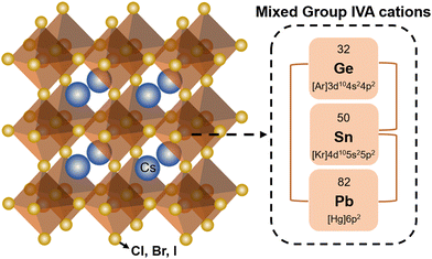
The general chemical formula of all-inorganic perovskites based on mixed group IVA cation is ABX3, where A is a monovalent cation (e.g. Cs+), B is a divalent cation (e.g. Pb2+, Sn2+, Ge2+), and X is a halide ion (e.g. I−, Br−). The ideal crystal structure of ABX3 can be regarded as a grid-like framework composed of BX6-octahedra connected at the corner-sharing vertices in three-dimensional space, and a large A-site is in the voids of a dodecahedron (Fig. 1). The structural stability of perovskites with various compositions can be given empirically by the Goldschmidt tolerance factor (t),38 | (1) |
Experimental and theoretical studies have revealed that the t value of the ABX3 perovskite generally ranges between 0.8 and 1. When the t value deviates from 1, other low-symmetry structures or nonperovskite phases are usually generated.39 Taking CsPbI3 as an example, γ-CsPbI3 (perovskite phase) can be transformed into δ-CsPbI3 (nonperovskite phase) at room temperature (RT) due to the low t value of 0.81.40,41 To obtain stable all-inorganic perovskites, the radius of divalent cations (B-site) should be less than that of lead so that the t value can approach 1. Several potential candidates for divalent cations inculde Ge2+, Sn2+, Cu2+, Ni2+, Co2+, Fe2+, Mn2+, etc. Sn and Ge are regarded as the key Pb substitutes due to their similar electronic structures. According to eqn (1), the value of t will increase gradually towards the perfect cubic phase when Sn or Ge is introduced to replace Pb entirely or partially.38
Electronic band structure
The valence band maximum (VBM) of the ABX3 perovskite is mainly determined by the formation of antibonding orbitals through hybridization between the B cation's s orbitals and the X anion's p orbitals, while the conduction band minimum (CBM) depends on the p orbitals of both the B cation and the X anion. The well-studied inorganic perovskite of CsPbI3 exhibits a bandgap of 1.73 eV, which exceeds the ideal-bandgap region (1.2–1.4 eV) according to the Shockley–Queisser limit.42 Replacing Pb with Sn or Ge with a smaller atom radius can significantly reduce the bandgap and increase the energy conversion efficiency. The experimentally derived bandgaps of CsSnI3 and CsGeI3 are 1.3 eV (ref. 43 and 44) and 1.6 eV, respectively.45 In addition, it is possible to further optimize the electronic band structures in CsSnI3 and CsGeI3. Transition metals with unfilled d orbitals can hybridize with the p orbitals of X anions, leading to an increase in the VBM and bandgap narrowing. For example, the indirect bandgaps of CsSnI3 can dramatically decrease when the replacement of partial Sn2+ ions with small-sized Cu2+ is over half.46The bandgaps of inorganic perovskites can also be effectively changed by the alloying strategy, which entails adjusting the mixing proportion of different ions at either B or X sites. For B-site alloying, benefited from the bowing effect, it is possible to form perovskite B-site alloys with even lower bandgaps than their pure-composition counterparts. This phenomenon has been exemplified by Pb–Sn alloying perovskites.47,48 Taking CsPbxSn1−xBr3 as an example, the bandgaps for CsPbBr3 and CsSnBr3 are 2.37 eV and 1.86 eV, respectively. While the bandgap change in the alloying perovskite is nonlinear in x with a bowing parameter of 0.9 eV, a low Pb content (x ∼ 0.3) in the alloying perovskite shows a much narrowed bandgap of 1.82 eV. Density functional theory (DFT) calculations reveal that this can be related to the crystal structure transformation. It is found that the orthorhombic phase of CsPbBr3 is in a tilted configuration. With the introduction of Sn2+ with a smaller ion radius, a lattice distortion is reduced, and the B–X–B bond angle gradually expands to 180°.49 For X-sitealloying in perovskites, anions exhibit increasing ionization energy and electron affinity from I−, Br− to Cl−, leading to a decrease in the B–X distance, and subsequently causing a large downward shift of the VBM.50,51 Apart from the bandgap factor, the stability issues resulted from anion mixing should also be considered. On one hand, the replacement of I− ions with Br− ions in perovskites can stabilize the perovskite phase. On the other hand, mixed-anion perovskites undergo phase segregation under light stimulus and the migration of halide ions can lead to the formation of in-gap trap states.52 For the A-site alloying in perovskites, it is generally considered that the A-site cations do not directly affect the bandgap, they can still impact the electronic band structures by possibly influencing the B–X bond length.53
All-inorganic PSC devices based on mixed group IVA cations
All-inorganic perovskites based on mixed group IVA cations possess several advantages in terms of phase stability and bandgaps. This section focuses mainly on the three types of perovskite compositions: CsPbxSn1−xIyBr3−y, CsPbxGe1−xIyBr3−y, and CsSnxGe1−xIyBr3−y. Among these, CsPbxSn1−xIyBr3−y is the most extensively studied composition due to the stability of Pb2+ in air. Accordingly, we summarize the performance improvement of all-inorganic CsPbxSn1−xIyBr3−y perovskites from the aspects of compositional engineering, morphology engineering, and additive engineering. Research studies on Sn and Ge-related perovskite compositions are still in their early phases, and only a handful of related studies have been reported, which will be reviewed in details. Furthermore, we will also discuss the research progress on perovskite nanomaterials of the above compositions.CsPbxSn1−xIyBr3−y perovskite
For example, Lee et al. fabricated an all-inorganic Sn-rich perovskite material, CsPb0.4Sn0.6I2.4Br0.6, with an excellent bandgap of 1.35 eV.58 The authors investigated the t value and defect formation energy of perovskite materials with different contents of Sn and Pb through DFT simulation. As the content of Sn2+ increased to 100%, the t value increased from 0.807 to 0.875, but the defect formation energy reached the lowest point when the content of Sn2+ decreased to 50%. Moreover, the authors investigated the humidity stability of perovskite samples with different Sn2+ contents by monitoring the evolution of X-ray diffraction (XRD) patterns, photoluminescence (PL) spectra, and ultraviolet–visible (UV-vis) spectra upon storage in a high-humidity environment for 1 h to several days. The results showed that CsPb0.4Sn0.6I3 has an even higher humidity stability compared to CsPbI3. Subsequently, the authors introduced Br− into CsPb0.4Sn0.6I3to prepare a perovskite material of CsPb0.4Sn0.6I2.4Br0.6, which shows a further improved structural stability together with a high tolerance to the thermal degradation caused by heat-induced strain.
Liang et al. prepared an all-inorganic Sn–Pb hybrid perovskite of CsPb0.9Sn0.1IBr2 in the ambient air,59 and revealed it has a narrow bandgap of 1.79 eV. CsPb0.9Sn0.1IBr2-based PSCs show a high open-circuit voltage (VOC) of 1.26 V and a PCE of 11.33%. In their devices, a layer of carbon electrode replaced the hole transport material (HTM) layer and the gold electrode, which not only avoided the use of expensive noble metal electrodes but also eliminated unstable organic components in the device. As a result, the encapsulated device exhibited negligible degradation after 3 months of storage at RT and remained operational after 2 weeks of heating at 100 °C. Even when exposed to the ambient air of 50–60% relative humidity (RH) for 50 h at RT, an unencapsulated device still maintains 85% of its initial PCE, demonstrating an improved moisture tolereance.
The quality of the perovskite films depends mainly on the preparation method. There are two commonly used fabrication methods, including one-step spin-coating and two-step deposition. However, it is difficult to control the stoichiometry of perovskite films with relatively complex compositions using two-step sequential deposition,59 making one-step deposition the preferred method for synthesizing inorganic perovskites with mixed group IVA cations. Li et al. used a one-step anti-solvent method to prepare CsPb1−xSnxIBr2 perovskite films.62 With an increase in the Sn content, there is a red shift in the UV-vis absorption spectrum of CsPb1−xSnxIBr2, indicating a smaller bandgap with a higher Sn content (Fig. 2a). The reduced bandgap of perovskite materials can absorb more photons and achieve a higher photocurrent under illumination. As the Sn content increases from 0 to 1, results based on scanning electron microscopy (SEM)show a clear effect of alloying on the quality of perovskite films. When the Sn content reaches 0.25, a perovskite film with a compact polycrystalline grain morphology is obtained. However, further increasing the Sn content can lead to an over-acceleration of the crystallization rate, causing an uncontrolled film quality. As a result, the number of pinholes in the perovskite film increases, and the surface becomes rough, leading to undesired carrier recombination and transport properties. Yang et al. found that the grain size of the perovskite films could reach the micrometer level with an increase in the Sn content.63 A similar phenomenon about the larger crystal size by increasing the Sn content can also be observed in CsPb1−xSnxI3-based perovskites (Fig. 2b–h). Similar to the earlier results,61 in the study by Yang et al., both PL and UV-vis spectra exhibit clear red shifts with an increase in the Sn content, and the short-circuit current density (JSC) increases due to the decreased bandgap. The devices with a structure of indium-doped tin oxide (ITO)/poly(3,4-ethylenedioxythiophene)poly(styrenesulfonate) (PEDOT:PSS)/CsSn0.3Pb0.7I3/[6,6]-phenyl-C61-butyric acid methyl ester (PCBM)/bathocuproine (BCP)/Ag exhibited a companion PCE of 9.4%. Besides, the authors also successfully fabricated HTM-free inverted devices based on CsSn0.3Pb0.7I3, which demonstrate a promising PCE of 7.6%.
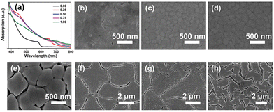 | ||
| Fig. 2 (a) UV-vis absorption spectra of CsPb1−xSnxIBr2 with varing x Reproduced from ref. 63 with permission from Wiley-VCH. Copyright 2018. Top-view SEM images of CsPb1−xSnxI3 films with (b) x = 0, (c) x = 0.25, (d) x = 0.30, (e) x = 0.50, (f) x = 0.75, (g) x = 0.88, and (h) x = 1.00. Reproduced from ref. 64 with permission from the American Chemical Society. Copyright 2020. | ||
Hu et al. employed a one-step spin-coating method without using an anti-solvent to prepare uniform CsPb0.6Sn0.4I3 perovskite films with good structural stability and high Sn2+ stability.64 However, these films remain vulnerable to water and show limited stability in the ambient air. To further improve the environmental stability, the authors first introduced a SnF2·3FACl additive into the CsPb0.6Sn0.4I3 precursor solution to functionalize the grain boundaries of perovskite thin films. Then, an organic salt, (aminomethyl) piperidinium diiodide (4AMP)I2, was used on the surface of CsPb0.6Sn0.4I3 to form a hydrophobic blocking layer and also to passivate the defects of perovskite thin films. Fig. 3a–c show the SEM images of the pristine perovskite film, the SnF2·3FACl incorperated perovskite film, and the SnF2·3FACl and (4AMP)I2 treated perovskite film, which are denoted as N-CsPb0.6Sn0.4I3, G-CsPb0.6Sn0.4I3, and G-S-CsPb0.6Sn0.4I3, respectively. The introduction of SnF2·3FACl can increase the grain size and reduce defect density, and the resulting UV-vis spectroscopy also shows improved absorption characteristics. The trap density of the perovskite films was estimated through space-current-limited-charge (SCLC) measurements.65,66 As shown in Fig. 3d, the trap-filled limited voltages (VTFL) are 1.11 V, 0.61 V, and 0.34 V for CsPb0.6Sn0.4I3, G-CsPb0.6Sn0.4I3, and G-S-CsPb0.6Sn0.4I3, respectively. The estimated trap densities for CsPb0.6Sn0.4I3, G-CsPb0.6Sn0.4I3, and G-S-CsPb0.6Sn0.4I3 are 5.50 × 10¹⁶, 3.02 × 10¹⁶, and 1.68 × 1016 cm−3, respectively. The device structure of fluorine-doped tin oxide (FTO)/NiOx/perovskite/PCBM/BCP/Ag was exploited. The devices based on CsPb0.6Sn0.4I3, G-CsPb0.6Sn0.4I3, and G-S-CsPb0.6Sn0.4I3 show PCEs of 0.92%, 5.68% and 11.28% (Fig. 3e), respectively. In terms of the continuous operation lifetime of the devices under one-sun illumination, after 1000 h of continuous operation, the device still retained 77% of its initial PCE.
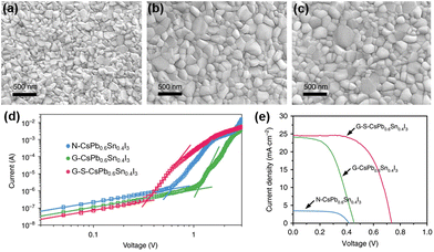 | ||
| Fig. 3 Top-view SEM images of (a) N-CsPb0.6Sn0.4I3, (b) G-CsPb0.6Sn0.4I3, and (c) G-S-CsPb0.6Sn0.4I3, (d) Dark I–V curves of N-CsPb0.6Sn0.4I3, G-CsPb0.6Sn0.4I3, and G-S-CsPb0.6Sn0.4I3 films, and (e) J–V curves of N-CsPb0.6Sn0.4I3, G-CsPb0.6Sn0.4I3, and G-S-CsPb0.6Sn0.4I3 devices. N-CsPb0.6Sn0.4I3, G-CsPb0.6Sn0.4I3, and G-S-CsPb0.6Sn0.4I3 refer to CsPb0.6Sn0.4I3 films without additional treatment, with SnF2·3FACl grain boundary treatment, and with both SnF2·3FACl and (4AMP)I2 treatments, respectively. Reproduced from ref. 64 with permission from Springer Nature. Copyright 2020. | ||
Chen et al. employed a one-step anti-solvent method for synthesizing a group of CsPb1−xSnxI2Br perovskites at a low annealing temperature (60 °C).68 As shown in Fig. 4a, CsPb0.55Sn0.45I2Br can exhibit the best thermal stability as compared to CsPbI2Br and MAPbI3 perovskite films under continuousannealing at 150 °C in an N2 glovebox. Then, Chen et al used CsCl and PbSO4 as additives and passivators, respectively, to improve the performance and stability of CsPb1−xSnxI2Br-based devices. The Cl- ions in CsCl help enlarge perovskite grains and also possibly fill iodine vacancies (VI), while PbSO4 acts as a passivation layer, which not only interacts with the uncoordinated Pb2+ to reduce defect-assisted carrier recombination but also forms a dense and hydrophobiccoating on the surface of the perovskite layer to prevent the intrusion of external oxygen and water as well as the migration of I−. The CsPb0.55Sn0.45I2Br–CsCl–PbSO4-based devices with a stacking structure of ITO/PEDOT:PSS/perovskite/PC61BM/Ag show the highest PCE of 10.39% with negligible hysteresis. Additionally, the CsPb0.55Sn0.45I2Br–CsCl–PbSO4-based device show outstanding shelf stability with 92.5% retention of initial PCE after 2000 h in an N2-filled glovebox, as compared to 72.66% for the CsPb0.55Sn0.45I2Br-based devices (Fig. 4b and c). Fig. 4d shows the operational stability (maximum-power-point tracking, MPPT) of unencapsulated devices with CsPb0.55Sn0.45I2Br, CsPb0.55Sn0.45I2Br–CsCl and CsPb0.55Sn0.45I2Br–CsCl–PbSO4 as the photoactive layers.
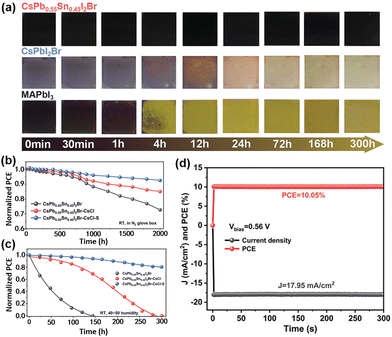 | ||
| Fig. 4 (a) Photographs of CsPb0.55Sn0.45I2Br, CsPbI2Br and MAPbI3 perovskite films under iso-thermal annealing (150 °C) in an N2-filled glove box. The long-term normalized PCE of PSCs (b) in an N2-filled glovebox and (c) in the ambient air (40–50% RH). (d) MPPT of a CsPb0.55Sn0.45I2Br-CsCl-S-based device. Reproduced from ref. 68 with permission from Wiley-VCH. Copyright 2021. | ||
The CsPb0.55Sn0.45I2Br–CsCl–PbSO4-based device retained 80% of its initial PCE after 300 h of continuous illumination, while the PCEs of CsPb0.55Sn0.45I2Br- and CsPb0.55Sn0.45I2Br–CsCl-based devices decreased to zero after 120 h and 280 h of continuous illumination, respectively.
A seed-assisted growth (SAG) method was used to fabricate a series of high-quality CsPb1−xSnxIBr2 films.69 To inhibit the oxidation of Sn2+ to Sn4+, reduce the trap density and improve the perovskite film morphology, zinc oxalate (ZnOx) was introduced into the perovskite precursor solution as an additive. Fig. 5a illustrates the photographs of perovskite solutions with/without ZnOx exposure to air. The color of the ZnOx-treated solution remained unchanged upon storage. In contrast, the control perovskite precursor solution turned reddish-brown from yellow after 72 h, indicating the inhibition of Sn2+ to Sn4+ due to the addition of ZnOx. Moreover, the oxidation product of the oxalate anion was CO2, avoiding the introduction of impurities into the perovskite film. Oxalate is an excellent ligand and can interact strongly with uncoordinated metal ions, as characterized by the Fourier-transform infrared (FTIR) spectra as shown in Fig. 5b. The coordination interaction can retard the crystallization of the perovskite, leading to a high-quality film. As shown in Fig. 5c, there are some pinholes and voids in the control film, while the ZnOx-treated film shows a full coverage with larger grains. Additionally, Zn2+ cations can refill Sn vacancies (VSn) and lead to vacancies (VPb) in the perovskite films. Besides, the introduction of ZnOx can reduce charge recombination and help to improve the device efficiency. As a result, the ZnOx-treated champion device shows a companion PCE of 14.1% with a hysteresis H-index of 4.2% as compared to the 12.9% PCE with a hysteresis H-index of 6.2% for the control device. The ZnOx-treated device also exhibit better long-term shelf lifetime and thermal stability than the control device.
 | ||
| Fig. 5 (a) Photographs confirming oxalate retarding the Sn2+ oxidation. (b) FTIR spectra and the characteristic regions of pure ZnOx, Pb/SnBr2, and Pb/SnBr2 + ZnOx in DMSO. (c) Top-view SEM images of CsPb0.7Sn0.3IBr2 thin films with and without ZnOx. Reproduced from ref. 67 with permission from Wiley-VCH, copyright 2022. | ||
SnF2 has been extensively used as an additive in Sn-based perovskites to retard the oxidation of Sn2+ to Sn4+.70–72 However, its uneven dispersion in the film would lead to the phase separation of the perovskite, resulting in a low-quality film.73 To address this issue, Ban et al. introduced tea polyphenol (TP) into the perovskite precursor solution to retard the oxidation of Sn2+ and modulate perovskite crystallization dynamics.74Fig. 6a shows the color evolution of the perovskite precursor solutions with/without TP (0.5 wt%) in air. The control film (without TP) exhibited a noticeable color variance from yellow to dark red (a typical color of Sn4+ solution) after 72 h of exposure to air, indicating the oxidation of Sn2+. In contrast, the TP-treated film showed no color change after the same period, indicateing that TP can retard the oxidation of Sn2+. In addition to slowing down the oxidation rate of Sn2+ to Sn4+, the coordination between TP and the perovskite, confirmed by FTIR characterization, can promote the crystallization of the perovskite, resulting in a uniform and dense high-quality film (Fig. 6b). As a result, the device with a structure of FTO/c-TiO2/CsPb0.5Sn0.5I2Br/Al2O3/NiO/carbon exhibits an improved PCE of 8.1% with the introduction of TP compared with that of 4.98% for a control device. In addition, the TP-treated device shows an improved shelf lifetime, maintaining 94% efficiency after 60 days of storage in a glovebox.
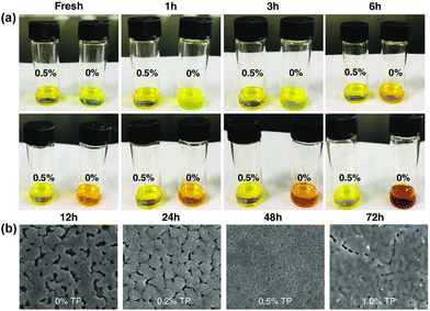 | ||
| Fig. 6 (a) Photographs of CsPb0.5Sn0.5I2Br precursor solutions with and without TP (0.5%). (b) Top-view SEM images of CsPb0.5Sn0.5I2Br thin films with varing TP contents. Reproduced from ref. 74 with permission from Wiley-VCH. Copyright 2020. | ||
CsPbxSn1−xI3 nanowires (NWs) were also synthesized by a two-step synthesis method,78 and their structure and phase transition properties were investigated by XRD (Fig. 7a). A series of XRD patterns of CsPbxSn1−xI3 indicate that there are no characteristic peaks of the starting material, and the characteristic peaks of the yellow (Y-) phase are similar to those of the nonperovskite phase of CsPbI3. After annealing, the generated black-γ (B-γ) phase (photoactive phase) perovskite NWs were obtained (Fig. 7b). The phase transition temperature of NWs with different Sn doping ratios was investigated, showing the growth trend with an increase in the lead content. Moreover, the bandgap of CsPbxSn1−xI3 NWs decreases with an increasein the Sn content. Electrical conductivity measurements showed that both Y-phase and B-phase NWs had higher conductivity with increasing Sn content, consistent with previous findings on the increased hole density in perovskites due to Sn vacancies.79 Moreover, the Seebeck coefficient measurement suggests that the CsPbxSn1−xI3 NWs are p-type semiconductors.
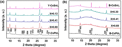 | ||
| Fig. 7 XRD patterns of (a) Y-phase CsPbxSn1−xI3 NWs and (b) B-γ phase CsPbxSn1−xI3 NWs. Reproduced from ref. 78 with permission from the American Chemical Society. Copyright 2018. | ||
CsPbxGe1−xIyBr3−y perovskite
Ge is a metal-like element in nature with relatively low toxicity compared to Pb. Thus, B-site alloying has also been explored for Pb–Ge based perovskites. Yang et al. introduced Ge into CsPbI2Br to fabricate CsPb1−xGexI2Br (x = 0, 0.1, 0.2, 0.3) perovskites at a low temperature (160 °C) in air with 50–60% RH.80 After an optimumaddition of Ge, the CsPb0.8Ge0.2I2Br perovskite film maintains the cubic perovskite phase under 50–60% RH for 120 h, while the cubic phase of the control all-inorganic perovskite film changes to the nonperovskite phase rapidly within 10 min. The CsPb0.8Ge0.2I2Br-based devices showed a champion PCE of 10.8% compared to that of 5.3% for the CsPbI2Br-based devices, which mainly resulted from the lower carrier recombination rate with the incorporation of Ge. In addition, the humidity stability of the device was also tested, and the performance of the device did not decrease after exposure to air with 50–60% RH for more than 7 h. For comparison, a rapid PCE decrease within 2 h is seen for the control CsPbI2Br-based device (Fig. 8).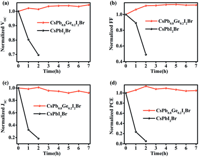 | ||
| Fig. 8 Stability tests of CsPb0.8Ge0.2I2Br and CsPbI2Br PSCs upon the storage in the ambient atmosphere (50--60 % RH): (a) VOC, (b) FF, (c) JSC, and (d) PCE. Reproduced from ref. 80 with permission from Wiley-VCH. Copyright 2018. | ||
Previous studies have shown that Ge is a potential element to replace Pb in Pb-less or even Pb-free perovskites. Because Cu2+ and Ge2+ possess the same ionic radius, Wang et al. used density functional theory (DFT) to study the effect of Ge/Cu binary co-doping on CsPbBr3-based perovskites.81 The authors examined the relationship between the lattice volume of CsPb1−xGexBr3 and CsPb1−xCuxBr3 (Fig. 9a). The higher strength of Cu–Br bonds in CsPb1−xCuxBr3 results in changes in bond lengths and bond angles, improving the charge transport properties of perovskites. When the content of Ge is greater than 27.5%, with the increase of Ge doping concentration, although the light absorption range is broadened, the CBM and VBM of CsPb1−xGexBr3 are larger than the oxidation potentials of H2O/H2 and H2O/O2, respectively, meaning that Ge2+ is easily oxidized to Ge4+ (Fig. 9b). The ability of Cu to redistribute charges allows it to extract electrons from the bulk phase of the perovskite. The formation energy of Cu on the surface is lower than that in the bulk phase due to the tendency of Vpb to appear on the perovskite surface. The Cu doping on the surface effectively inhibits the erosion of the perovskite by moisture. This moisture resistance can be achieved by increasing the doping amount of Cu, and more Cu/Ge doping not only reduces the toxic Pb content but also improves the light absorption in the visible light wavelength range.
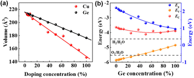 | ||
| Fig. 9 (a) Normalized volumes of Ge- and Cu-doped bulk CsPbBr3. (b) Bandgap coupled to the energies of the VBM and the CBM for CsPb1−xGexBr3. Reproduced from ref. 81 with permission from the American Chemical Society. Copyright 2021. | ||
CsSnxGe1−xIyBr3−y perovskite
Since Ge replaces part of Sn in CsSnI3, the t value of the perovskite reaches 0.94, leading to a high stability of the lattice structure. Chen et al. used the one-step vapor-processing method to fabricate Pb-free CsSn0.5Ge0.5I3.82 Moreover, the extremely high oxidation activity of Ge(II) can form an ultrathin uniform natural oxide surface passivation layer on the surface of the perovskite film after exposing to an ambient atmosphere for 30 s, which is GeO2 as indicated by X-ray photoelectron spectroscopy (XPS) analysis (Fig. 10). The as-obtained perovskite powders remain phase-stable whether directly exposed to high-humidity air or subjected to continuous one-sun illumination. CsSn0.5Ge0.5I3-based devices with a configuration of FTO/PCBM/CsSn0.5Ge0.5I3/spiro/Au show a champion PCE of 7.11%. Moreover, after 500 h of continuous operation under a nitrogen atmosphere, the unencapsulated device can maintain 92% of its initial PCE. Subsequently, several research groups have evaluated tin–germanium hybrid all-inorganic perovskites from the perspectives of the crystal structure, optoelectronic properties, and defect properties based on first-principles calculations.83–86 Through simulation calculations, it is found that the alloy with Ge/Sn = 1 shows the best optical absorption and benign defects. Ge doping has a remarkable effect on eliminating deep defects, which provides new insights into the evolution and regulation of defect properties.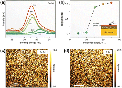 | ||
| Fig. 10 (a) Ge 3d XPS spectra at different incidence angles in a vapor-deposited CsSn0.5Ge0.5I3 film. (b) The corresponding plot of the Ge(II) fraction vs. the incidence angle. (c) and (d) XPS maps of Ge 3d (33 eV) and O 1s (532 eV). Reproduced from ref. 82 with permission from Springer Nature. Copyright 2020. | ||
Liu et al. first fabricated all-inorganic Sn–Ge alloy perovskite nanocrystals (PNCs) using the hot injection method.86 Compared with Sn-based PNCs, these Sn–Ge-based PNCs exhibited significantly improved optical properties, and the stability of perovskites was also effectively enhanced. The partial substitution of Sn atoms by Ge in PNCs can effectively fill the high density of VSn and reduce surface traps, thereby prolonging the exciton lifetime and improving the photoluminescence quantum yields (PLQYs). Although the adding amounts of SnI2 and GeI2 are equal in the synthesis of PNCs, the results indicated that the substitution ratio of Ge does not reach 50%. Therefore, the authors determine the final light-absorbing layer component as CsSn0.6Ge0.4I3. In both UV-vis and PL results, an obvious blue-shift is observed, and the PL of CsSn0.6Ge0.4I3 had a sub-peak at 725 nm in addition to the main peak at 780 nm (Fig. 11a). The authors speculated that there are a small amount of carbon nanorods in addition to PNCs. Time-resolved photoluminescence (TRPL) test results show that the carrier lifetime of CsSn0.6Ge0.4I3 is longer than that of CsSnI3, indicating that Ge incorperation leads to a lower defect concentration. This supports the hypothesis that Ge2+ with a smaller ionic radius easily fills the VSn, reducing the density of defects (Fig. 11b). Conventional devices with a structure of FTO/c-TiO2/CsSn0.6Ge0.4I3/spiro-OMeTAD/MoO3/Au were assembled. The resulting Sn–Ge PNC-based devices show a champion PCE of 4.9% with negligible hysteresis. Moreover, the introduction of Ge can help the improvement of long-term stability because of the inhibition of Sn2+ oxidation.
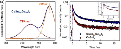 | ||
| Fig. 11 (a) Steady-state PL spectra of CsSn0.6Ge0.4I3 NCs. (b) TRPL spectra of CsSn0.6Ge0.4I3 and CsSnI3. Reproduced from ref. 86 with permission from Wiley-VCH, copyright 2020. | ||
Conclusion and outlook
In summary, all-inorganic mixed group IVA cation perovskites have attracted growing attention due to their potentially high stability and environmental friendliness, leading to promising device performance parameters as presented in Table 1. Nevertheless, there is still a significant gap between their actual device performance and that of state-of-the-art perovskites. We envision that future research efforts in the following directions will contribute to filling the gap.| Devices structure | V OC (V) | J SC (mA cm−2) | FF | PCE (%) | Stability (conditions) | Ref. |
|---|---|---|---|---|---|---|
| FTO/c-TiO2/m-TiO2/CsPb0.9Sn0.1IBr2/carbon | 1.26 | 14.30 | 0.63 | 11.33 | >300 h (encapsulated, 100 °C) | 55 |
| FTO/c-TiO2/m-TiO2/CsPb0.4Sn0.6IBr2 QDs/spiro/Au | 0.63 | 10.13 | 0.46 | 2.9 | >1 month (30%–40% RH, RT) | 75 |
| ITO/SnO2/C60/CsPb0.75Sn0.25IBr2/spiro/Au | 1.21 | 12.57 | 0.76 | 11.53 | Maintaining 80% of its initial PCE after storing for 1000 h (50–60% RH encapsulated, RT) | 58 |
| ITO/PEDOT/PSS/CsPb0.7Sn0.3IBr2/PCBM/(BCP)/Ag | 0.64 | 20.96 | 0.7 | 9.41 | Maintaining 97% of its initial PCE after storing for 6 months and maintaining 94.86% of its initial PCE after 186 h continuous illumination (in a nitrogen-filled glovebox) | 63 |
| FTO/c-TiO2/m-TiO2/CsPb0.5Sn0.5I2Br/Al2O3/NiO/carbon | 0.61 | 20.1 | 0.65 | 8.1 | Maintaining 94% of its initial PCE after storing for 60 days and maintaining 90.1% of its initial PCE for 200 h MPPT (in a nitrogen-filled glovebox) | 72 |
| FTO/NiOx/CsPb0.6Sn0.4I3/PCBM/Ag | 0.774 | 25.87 | 0.67 | 13.37 | No PCE degradation after storing for 2800 h (dry, N2, RT) | 64 |
| ITO/SnO2/CsPb0.7Sn0.3IBr2/PCBM/Ag | 1.18 | 15.5 | 0.77 | 14.1 | Maintaining 75% of its initial PCE after storing for 10 days (in air, RT) | 67 |
| ITO/PEDOT:PSS/CsPb0.55Sn0.45I2Br/sulfate/PCB61M/BCP/Ag | 0.7 | 20.57 | 0.72 | 10.39 | Maintaining 80% of its initial PCE for 300 h MPPT (in air, 40–50% RH) | 66 |
| FTO/PCBM/CsSn0.5Ge0.5I3/spiro/Au | 0.63 | 18.61 | 0.61 | 7.11 | Maintaining 92% of its initial PCE for 500 h continuous operation (N2, 45 °C) | 80 |
| FTO/c-TiO2/CsSn0.6Ge0.4I3 NCs/spiro/MoO3/Au | 0.65 | 11.8 | 0.64 | 4.9 | 84 | |
| FTO/SnO2/CsPb0.8Ge0.2I2Br/P3HT/spiro/Au | 1.27 | 12.15 | 0.7 | 10.8 | No PCE degradation after storing for 7 h (in air, 50–60 RH) | 78 |
From the perspective of materials science, understanding and tailoring morphological defects such as grain boundaries, intragrain defects, and surfaces/heterointerfaces in these perovskites are critical to optimizing the properties and device performance. The inclusion of Sn and Ge cations has been found to significantly influence crystallization kinetics, while the mechanisms have not been elucidated. Multimodal characterization techniques with high spatiotemporal resolutions concerning the particular material characteristics of these perovskites needs to be developed and employed.
From the perspective of device sciences, the relatively high VOC deficit needs to be addressed via novel interface designs. Particularly, perovskites containing Sn or Ge cations generally produce narrower bandgaps and thus wider light absorption than pure Pb perovskites, making the JSC of the resulting devices advantageous. However, these perovskites tend to exhibit higher trap densities and less ideal band alignments in devices, leading to more severe non-radiative recombination. In this context, creating benign device interfaces with a range of organic, inorganic, and hybrid materials is necessary to overcome the VOC bottleneck. In addition to generic interface design rules, we should take the unique oxidation issues for Sn or Ge into consideration.
Conflicts of interest
There are no conflicts to declare.Acknowledgements
Z. Z., Y. L. and W. J. thank the Taishan Scholars Project of Shandong Province (Grant No. 201909121) and the Introduction and Cultivation Plan of Young Innovative Talents in Colleges and Universities of Shandong Province (2019). Y. Z., T. D. and C. Y. acknowledge the Early Career Scheme (No. 22300221), the General Research Fund (No. 12302822) from the Hong Kong Research Grant Council (RGC), and the Excellent Young Scientists Funds (No. 52222318) from the National Natural Science Foundation of China. Y. Z., T. D. and C. Y. also acknowledge the start-up grants, Initiation Grant – Faculty Niche Research Areas (RC-FNRA-IG/20-21/SCI/06), Interdisciplinary Research Matching Scheme (IRMS/20-21/02) and Matching Proof-of Concept Fund (MPCF-001-2022-23) of HKBU. T. D. acknowledges the support from the Hong Kong RGC Postdoctoral Fellowship.References
- K. Galkowski, A. Mitioglu, A. Miyata, P. Plochocka, O. Portugall, G. E. Eperon, J. T. W. Wang, T. Stergiopoulos, S. D. Stranks, H. J. Snaith and R. J. Nicholas, Energy Environ. Sci., 2016, 9, 962–970 RSC.
- T. Baikie, Y. Fang, J. M. Kadro, M. Schreyer, F. Wei, S. G. Mhaisalkar, M. Grätzel and T. J. White, J. Mater. Chem. A, 2013, 1, 5628–5641 RSC.
- Q. Dong, Y. Fang, Y. Shao, P. Mulligan, J. Qiu, L. Cao and J. Huang, Science, 2015, 347, 967–970 CrossRef CAS PubMed.
- J. Tong, Z. Song, D. H. Kim, X. Chen, C. Chen, A. F. Palmstrom, P. F. Ndione, M. O. Reese, S. P. Dunfield, O. G. Reid, J. Liu, F. Zhang, S. P. Harvey, Z. Li, S. T. Christensen, G. Teeter, D. Zhao, M. M. Al-Jassim, M. F. A. M. V. Hest, M. C. Beard, S. E. Shaheen, J. J. Berry, Y. Yan and K. Zhu, Science, 2019, 364, 475–479 CrossRef CAS PubMed.
- D. Ma, K. Lin, Y. Dong, H. Choubisa, A. H. Proppe, D. Wu, Y. Wang, B. Chen, P. Li, J. Z. Fan, F. Yuan, A. Johnston, Y. Liu, Y. Kang, Z. H. Lu, Z. Wei and E. H. Sargent, Nature, 2021, 599, 594–598 CrossRef CAS PubMed.
- R. Lin, J. Xu, M. Wei, Y. Wang, Z. Qin, Z. Liu, J. Wu, K. Xiao, B. Chen, S. M. Park, G. Chen, H. R. Atapattu, K. R. Graham, J. Xu, J. Zhu, L. Li, C. Zhang, E. H. Sargent and H. Tan, Nature, 2022, 603, 73–78 CrossRef CAS PubMed.
- X. Lin, H. Su, S. He, Y. Song, Y. Wang, Z. Qin, Y. Wu, X. Yang, Q. Han, J. Fang, Y. Zhang, H. Segawa, M. Grätzel and L. Han, Nat. Energy, 2022, 7, 520–527 CrossRef CAS.
- X. Zhao, T. Liu, Q. C. Burlingame, T. Liu, R. Holleylll, G. Cheng, N. Yao, F. Gao and Y.-L. Loo, Science, 2022, 377, 307–310 CrossRef CAS PubMed.
- K. Xiao, Y.-H. Lin, M. Zhang, R. D. J. Oliver, X. Wang, Z. Liu, X. Luo, J. Li, D. Lai, H. Luo, R. Lin, J. Xu, Y. Hou, H. J. Snaith and H. Tan, Science, 2022, 376, 762–767 CrossRef CAS PubMed.
- Z. Li, B. Li, X. Wu, S. A. Sheppard, S. Zhang, D. Gao, N. J. Long and Z. Zhu, Science, 2022, 376, 416–420 CrossRef CAS PubMed.
- X. Li, W. Zhang, X. Guo, C. Lu, J. Wei and J. Fang, Science, 2022, 375, 434–437 CrossRef CAS PubMed.
- N. Li, X. Niu, L. Li, H. Wang, Z. Huang, Y. Zhang, Y. Chen, X. Zhang, C. Zhu, H. Zai, Y. Bai, S. Ma, H. Liu, X. Liu, Z. Guo, G. Liu, R. Fan, H. Chen, J. Wang, Y. Lun, X. Wang, J. Hong, H. Xie, D. S. Jakob, X. G. Xu, Q. Chen and H. Zhou, Science, 2021, 373, 561–567 CrossRef CAS PubMed.
- Y. Zou, P. Teng, W. Xu, G. Zheng, W. Lin, J. Yin, L. Kobera, S. Abbrent, X. Li, J. A. Steele, E. Solano, M. B. J. Roeffaers, J. Li, L. Cai, C. Kuang, I. G. Scheblykin, J. Brus, K. Zheng, Y. Yang, O. F. Mohammed, O. M. Bakr, T. Pullerits, S. Bai, B. Sun and F. Gao, Nat. Commun., 2021, 12, 4831 CrossRef CAS PubMed.
- W. Kim, H. Kim, T. J. Yoo, J. Y. Lee, J. Y. Jo, B. H. Lee, A. A. Sasikala, G. Y. Jung and Y. Pak, Nat. Commun., 2022, 13, 720 CrossRef CAS PubMed.
- Y. J. Li, Y. Lv, C.-L. Zou, W. Zhang, J. Yao and Y. S. Zhao, J. Am. Chem. Soc., 2016, 138(7), 2122–2125 CrossRef CAS PubMed.
- A. Kojima, K. Teshima, Y. Shirai and T. Miyasaka, J. Am. Chem. Soc., 2009, 131(17), 6050–6051 CrossRef CAS PubMed.
- https://www.nrel.gov/pv/cell-efficiency.html .
- J. Huang, S. Tan, P. D. Lund and H. Zhou, Energy Environ. Sci., 2017, 10, 2284–2311 RSC.
- T. Leijtens, K. Bush, R. Cheacharoen, R. Beal, A. Bowring and M. D. McGehee, J. Mater. Chem. A, 2017, 5, 11483–11500 RSC.
- E. T. Hoke, D. J. Slotcavage, E. R. Dohner, A. R. Bowring, H. I. Karunadasa and M. D. McGehee, Chem. Sci., 2015, 6, 613–617 RSC.
- J. A. Christians, P. Schulz, J. S. Tinkham, T. H. Schloemer, S. P. Harvey, B. J. T. de Villers, A. Sellinger, J. J. Berry and J. M. Luther, Nat. Energy, 2018, 3, 68–74 CrossRef CAS.
- Y. Wang, M. I. Dar, L. K. Ono, T. Zhang, M. Kan, Y. Li, L. Zhang, X. Wang, Y. Yang, X. Gao, Y. Qi, M. Grätzel and Y. Zhao, Science, 2019, 365, 591–595 CrossRef CAS PubMed.
- P. Wang, X. Zhang, Y. Zhou, Q. Jiang, Q. Ye, Z. Chu, X. Li, X. Yang, Z. Yin and J. You, Nat. Commun., 2018, 9, 2225 CrossRef PubMed.
- X. Sun, Z. Shao, Z. Li, D. Liu, C. Gao, C. Chen, B. Zhang, L. Hao, Q. Zhao, Y. Li, X. Wang, Y. Lu, X. Wang, G. Cui and S. Pang, Joule, 2022, 6, 850–860 CrossRef CAS.
- M. Kulbak, D. Cahen and G. Hodes, J. Phys. Chem. Lett., 2015, 6, 2452–2456 CrossRef CAS PubMed.
- Y. Cui, J. Shi, F. Meng, B. Yu, S. Tan, S. He, C. Tan, Y. Li, H. Wu, Y. Luo, D. Li and Q. Meng, Adv. Mater., 2022, 34, 2205028 CrossRef CAS PubMed.
- J. Rödel, W. Jo, K. T. P. Seifert, E.-M. Anton, T. Granzow and D. Damjanovic, J. Am. Chem. Soc., 2009, 92, 1153–1177 Search PubMed.
- J. Tian, Q. Xue, Q. Yao, N. Li, C. J. Brabec and H.-L. Yip, Adv. Energy Mater., 2020, 10, 2000183 CrossRef CAS.
- Q. Tai, K.-C. Tang and F. Yan, Energy Environ. Sci., 2019, 12, 2375–2405 RSC.
- M. B. Faheem, B. Khan, C. Feng, M. U. Farooq, F. Raziq, Y. Xiao and Y. Li, ACS Energy Lett., 2020, 5(1), 290–320 CrossRef CAS.
- J. Chen and W. C. H. Choy, Sol. RRL, 2020, 4, 2000408 CrossRef CAS.
- Y. Yuan, G. Yan, R. Hong, Z. Liang and T. Kirchartz, Adv. Mater., 2022, 34, 2108132 CrossRef CAS PubMed.
- J. Liang and Y. B. Qi, Mater. Today Nano, 2021, 16, 100143 CrossRef CAS.
- O. O. Bello and M. E. Emetere, Sol. Energy, 2022, 243, 370–380 CrossRef CAS.
- M. Ikram, R. Malik, R. Raees, M. Imran, F. Wang, S. Ali, M. Khan, Q. Khan and M. Maqbool, Sustain. Energy Technol. Assess., 2022, 53, 102433 Search PubMed.
- A. Wang, C. Zuo, X. Niu, L. Ding, J. Ding and F. Hao, Chem. Eng. J., 2023, 451, 138926 CrossRef CAS.
- H. Wei, P. Qiu, Y. Li, Y. Li, M. Peng, X. Zheng and X. Liu, Ceram. Int., 2022, 48, 5876–5891 CrossRef CAS.
- M. Zhu, C. Li, B. Li, J. Zhang, Y. Sun, W. Guo, Z. Zhou, S. Pang and Y. Yan, Mater. Horiz., 2020, 7, 2208–2236 RSC.
- J. Y. Kim, J.-W. Lee, H. S. Jung, H. Shin and N.-G. Park, Chem. Rev., 2020, 120(15), 7867–7918 CrossRef CAS PubMed.
- A. Marronnier, G. Roma, S. Boyer-Richard, L. Pedesseau, J.-M. Jancu, Y. Bonnassieux, C. Katan, C. C. Stoumpos, M. G. Kanatzidis and J. Even, ACS Nano, 2018, 12(4), 3477–3486 CrossRef CAS PubMed.
- R. J. Sutton, M. R. Filip, A. A. Haghighirad, N. Sakai, B. Wenger, F. Giustino and H. J. Snaith, ACS Energy Lett., 2018, 3(8), 1787–1794 CrossRef CAS.
- Z. Xiao, Y. Zhou, H. Hosono, T. Kamiya and N. P. Padture, Chem. – Eur. J., 2018, 24, 2305–2316 CrossRef CAS PubMed.
- M. H. Kumar, S. Dharani, W. L. Leong, P. P. Boix, R. R. Prabhakar, T. Baikie, C. Shi, H. Ding, R. Ramesh, M. Asta, M. Grätzel, S. G. Mhaisalkar and N. Mathews, Adv. Mater., 2014, 26, 7122–7127 CrossRef CAS PubMed.
- T. C. Jellicoe, J. M. Richter, H. F. J. Glass, M. Tabachnyk, R. Brady, S. E. Dutton, A. Rao, R. H. Friend, D. Credgington, N. C. Greenham and M. L. Böhm, J. Am. Chem. Soc., 2016, 138, 2941–2944 CrossRef CAS PubMed.
- X. Wu, W. Song, Q. Li, X. Zhao, D. He and Z. Quan, Chem. – Asian J., 2018, 13, 1654–1659 CrossRef CAS PubMed.
- M. N. Islam, J. Podder and M. L. Ali, RSC Adv., 2021, 11, 39553–39563 RSC.
- F. Hao, C. C. Stoumpos, R. P. H. Chang and M. G. Kanatzidis, J. Am. Chem. Soc., 2014, 136(22), 8094–8099 CrossRef CAS PubMed.
- A. Rajagopal, R. J. Stoddard, H. W. Hillhouse and A. K.-Y. Jen, J. Mater. Chem. A, 2019, 7, 16285–16293 RSC.
- H. A. Schwartz, H. Laurenzen, A. Marzouk, M. Runkel, K. O. Brinkmann, D. Rogalla, T. Riedl, S. Ashhab and S. Olthof, ACS Appl. Mater. Interfaces, 2021, 13, 4203–4210 CrossRef CAS PubMed.
- S. Tao, I. Schmidt, G. Brocks, J. Jiang, I. Tranca, K. Meerholz and S. Olyhof, Nat. Commun., 2019, 10, 2560 CrossRef PubMed.
- R. M. I. Bandara, S. M. Silva, C. C. L. Underwood, K. D. G. I. Jayawardena, R. A. Sporea and S. R. P. Silva, Energy Environ. Mater., 2022, 5, 370–400 CrossRef CAS.
- D. J. Slotcavage, H. I. Karunadasa and M. D. McGehee, ACS Energy Lett., 2016, 1, 1199–1205 CrossRef CAS.
- L. A. Muscarella, E. M. Hutter, F. Wittmann, Y. W. Woo, Y.-K. Jung, L. McGovern, J. Versluis, A. Walsh, H. J. Bakker and B. Ehrler, ACS Energy Lett., 2020, 5, 3152–3158 CrossRef CAS PubMed.
- M. Hu, G. Wang, Q. Zhang, J. Gong, Z. Xing, J. Gao, J. Wang, P. Zeng, S. Zheng, M. Liu, Y. Zhou and S. Yang, J. Energy Chem., 2022, 72, 487–494 CrossRef CAS.
- H. Yan, J. Huang, X. Zhang, M. Wang, J. Liu, C. Meng, S. Deng, L. Lu, P. Xu, H.-S. Kwok and G. Li, Sol. RRL, 2022, 6, 2100899 CrossRef CAS.
- C.-H. Kuan, H.-H. Shen and C.-F. Lin, RSC Adv., 2021, 11, 3264–3271 RSC.
- A. Swarnkar, W. J. Mir and A. Nag, ACS Energy Lett., 2018, 3, 286–289 CrossRef CAS.
- S. Lee, J. Moon, J. Ryu, B. Parida, S. Yoon, D.-G. Lee, J. S. Cho, S. Hayase and D.-W. Kang, Nano Energy, 2020, 77, 105309 CrossRef CAS.
- J. Liang, P. Zhao, C. Wang, Y. Wang, Y. Hu, G. Zhu, L. Ma, J. Liu and Z. Jin, J. Am. Chem. Soc., 2017, 139(40), 14009–14012 CrossRef CAS PubMed.
- N. Y. Nia, F. Giordano, M. Zendehdel, L. Cinà, A. L. Palma, P. G. Medaglia, S. M. Zakeeruddin, M. Grätzel and A. D. Carlo, Nano Energy, 2020, 69, 104441 CrossRef.
- T. Salim, S. Sun, Y. Abe, A. Krishna, A. C. Grimsdale and Y. M. Lam, J. Mater. Chem. A, 2015, 3, 8943–8969 RSC.
- N. Li, Z. Zhu, J. Li, A. K.-Y. Jen and L. Wang, Adv. Energy Mater., 2018, 8, 1800525 CrossRef.
- Z. Yang, X. Zhang, W. Yang, G. E. Eperon and D. S. Ginger, Chem. Mater., 2020, 32(7), 2782–2794 CrossRef CAS.
- M. Hu, M. Chen, P. Guo, H. Zhou, J. Deng, Y. Yao, Y. Jiang, J. Gong, Z. Dai, Y. Zhou, F. Qian, X. Chong, J. Feng, R. D. Schaller, K. Zhu, N. P. Padture and Y. Zhou, Nat. Commun., 2020, 11, 151 CrossRef CAS PubMed.
- Z. Zhou, Z. Qiang, T. Sakamaki, I. Takei, R. Shang and E. Nakamura, ACS Appl. Mater. Interfaces, 2019, 11(25), 22603–22611 CrossRef CAS PubMed.
- J. Zhan, M. Li and Z. Zhou, Sol. RRL, 2022, 2200082 CrossRef CAS.
- Y. Ahmed, B. Khan, M. B. Faheem, K. Huang, Y. Gao and J. Yang, J. Energy Chem., 2022, 67, 361–390 CrossRef CAS.
- G. Chen, P. Li, T. Xue, M. Su, J. Ma, Y. Zhang, T. Wu, L. Han, M. Aldamasy, M. Li, Z. Li, J. Ma, S. Chen, Y. Zhao, F. Wang and Y. Song, Small, 2021, 17, 2101380 CrossRef CAS PubMed.
- W. Zhang, H. Liu, X. Qi, Y. Yu, Y. Zhou, Y. Xia, J. Cui, Y. Shi, R. Chen and H.-L. Wang, Adv. Sci., 2022, 9, 2106054 CrossRef CAS PubMed.
- E. W.-G. Diau, E. Jokar and M. Rameez, ACS Energy Lett., 2019, 4(8), 1930–1937 CrossRef CAS.
- J. Pascual, M. Flatken, R. Félix, G. Li, S.-H. Turren-Cruz, M. H. Aldamasy, C. Hartmann, M. Li, D. D. Girolamo, G. Nasti, E. Hüsam, R. G. Wilks, A. Dallmann, M. Bär, A. Hoell and A. Abate, Angew. Chem., Int. Ed., 2021, 60, 21583–21591 CrossRef CAS PubMed.
- T. M. Koh, T. Krishnamoorthy, N. Yantara, C. Shi, W. L. Leong, P. P. Boix, A. C. Grimsdale, S. G. Mhaisalkar and N. Mathews, J. Mater. Chem. A, 2015, 3, 14996–15000 RSC.
- S. J. Lee, S. S. Shin, Y. C. Kim, D. Kim, T. K. Ahn, J. H. Noh, J. Seo and S. I. Seok, J. Am. Chem. Soc., 2016, 138(12), 3974–3977 CrossRef CAS PubMed.
- H. Ban, Q. Sun, T. Zhang, H. Li, Y. Shen and M. Wang, Sol. RRL, 2020, 4, 1900457 CrossRef CAS.
- A. Swarnk, A. R. Marshall, E. M. Sanehira, B. D. Chernomordik, D. T. Moore, J. A. Christians, T. Chakrabarti and J. M. Luther, Science, 2016, 354, 92–95 CrossRef PubMed.
- J. Yuan, C. Bi, J. Xi, R. Guo and J. Tian, J. Phys. Chem. Lett., 2021, 12(3), 1018–1024 CrossRef CAS PubMed.
- F. Liu, C. Ding, Y. Zhang, T. S. Ripolles, T. Kamisaka, T. Toyoda, S. Hayase, T. Minemoto, K. Yoshino, S. Dai, M. Yanagida, H. Noguchi and Q. Shen, J. Am. Chem. Soc., 2017, 139(46), 16708–16719 CrossRef CAS PubMed.
- T. Lei, M. Lai, Q. Kong, D. Lu, W. Lee, L. Dou, V. Wu, Y. Yu and P. Yang, Nano Lett., 2018, 18(6), 3538–3542 CrossRef CAS PubMed.
- I. Chung, J.-H. Song, J. Im, J. Androulakis, C. D. Malliakas, H. Li, A. J. Freeman, J. T. Kenney and M. G. Kanatzidis, J. Am. Chem. Soc., 2012, 134(20), 8579–8587 CrossRef CAS PubMed.
- F. Yang, D. Hirotani, G. Kapil, M. A. Kamarudin, C. H. Ng, Y. Zhang, Q. Shen and S. Hayase, Angew. Chem., Int. Ed., 2018, 57, 12745–12749 CrossRef CAS PubMed.
- L. Wang, J. Su, Y. Guo, Z. Lin, Y. Hao and J. Chang, J. Phys. Chem. Lett., 2021, 12(3), 1098–1103 CrossRef CAS PubMed.
- M. Chen, M.-G. Ju, H. F. Garces, A. D. Carl, L. K. Ono, Z. Hawash, Y. Zhang, T. Shen, Y. Qi, R. L. Grimm, D. Pacifici, X. C. Zeng, Y. Zhou and N. P. Padture, Nat. Commun., 2019, 10, 16 CrossRef CAS PubMed.
- F. Valadares, I. Guilhon, L. K. Teles and M. Marques, J. Phys. Chem. C, 2021, 125(39), 21740–21747 CrossRef CAS.
- J. Chang, L. Jiang, G. Wang, W. Zhao, Y. Huang and H. Chen, Phys. Chem. Chem. Phys., 2021, 23, 14449–14456 RSC.
- Y. Raoui, S. Kazim, Y. Galagan, H. Ez-Zahraouyc and S. Ahmad, Sustainable Energy Fuels, 2021, 5, 4661–4667 RSC.
- M. Liu, H. Pasanen, H. Ali-Löytty, A. Hiltunen, K. Lahtonen, S. Qudsia, J.-H. Smått, M. Valden, N. V. Tkachenko and P. Vivo, Angew. Chem., Int. Ed., 2020, 59, 22117–22125 CrossRef CAS PubMed.
| This journal is © The Royal Society of Chemistry 2023 |


