DOI:
10.1039/D2NR07252A
(Review Article)
Nanoscale, 2023,
15, 7227-7248
Localised strain and doping of 2D materials
Received
27th December 2022
, Accepted 28th March 2023
First published on 28th March 2023
Abstract
There is a growing interest in 2D materials-based devices as the replacement for established materials, such as silicon and metal oxides in microelectronics and sensing, respectively. However, the atomically thin nature of 2D materials makes them susceptible to slight variations caused by their immediate environment, inducing doping and strain, which can vary between, and even microscopically within, devices. One of the misapprehensions for using 2D materials is the consideration of unanimous intrinsic properties over different support surfaces. The interfacial interaction, intrinsic structural disorder and external strain modulate the properties of 2D materials and govern the device performance. The understanding, measurement and control of these factors are thus one of the significant challenges for the adoption of 2D materials in industrial electronics, sensing, and polymer composites. This topical review provides a comprehensive overview of the effect of strain-induced lattice deformation and its relationship with physical and electronic properties. Using the example of graphene and MoS2 (as the prototypical 2D semiconductor), we rationalise the importance of scanning probe techniques and Raman spectroscopy to elucidate strain and doping in 2D materials. These effects can be directly and accurately characterised through Raman shifts in a non-destructive manner. A generalised model has been presented that deconvolutes the intertwined relationship between strain and doping in graphene and MoS2 that could apply to other members of the 2D materials family. The emerging field of straintronics is presented, where the controlled application of strain over 2D materials induces tuneable physical and electronic properties. These perspectives highlight practical considerations for strain engineering and related microelectromechanical applications.
1. Fundamentals of strain and doping
1.1. Susceptibility of 2D materials for strain and doping
The isolation of graphene in 2004 unleashed the veracity of thermodynamic stability in two-dimensional (2D) materials. One of the plausible explanations for their existence in the real world as 2D crystals is due to the rearrangements of atoms through structural distortions such as gentle crumbling or stretching.26 However, these distortions influence the electronic properties and often alter the energy band gap.32 For example, the physical deposition of 2D materials over a substrate of certain roughness and dielectric constant can lead to super-lubricious contact,36 regulated out-of-plane deformation,38 pseudo-magnetic field39 or confinement effects,40 depending on the type of the interfacial interactions (van der Waals, ionic or covalent).41 The surface atoms of 2D materials are also directly exposed to the local environment such as airborne impurities, chemical analytes and substrates, and are thus susceptible to mechanical strain, doping and/or strain-induced doping.14 Therefore, these structural distortions and the influence of the surroundings play a crucial role to govern their localised physical and electronic characteristics.
Graphene is considered an ideal prototypical example of an atomic 2D system due to the combination of extreme elastic deformability (up to 25%),42 high room-temperature charge mobility (μ = 15![[thin space (1/6-em)]](https://www.rsc.org/images/entities/char_2009.gif) 000 cm2 V−1 s−1), and linear energy–momentum dispersion relation at Dirac point.26 Graphene is sensitive towards its host surface that serves as a support; even a cleaned silica substrate with minimal roughness (in picometers) and trapped charges in the oxide layer exhibits high electron–hole charge puddles to graphene under a strain variation comparable to the length scale that causes localised charge fluctuations leading to variation in the energy of the Dirac point.43 These unique features make graphene an excellent candidate to study pivotal aspects of strain such as deformed lattice-induced band-gap engineering, superconducting phenomena, topotronics and straintronics.1,44 Moreover, the endeavour of graphene research encourages the exploration of other 2D families such as group-VI transition metal dichalcogenides (TMDs), MXenes, 2D perovskite,45 2D-Xenes (X = Si, Ge, Sn) and so on.46
000 cm2 V−1 s−1), and linear energy–momentum dispersion relation at Dirac point.26 Graphene is sensitive towards its host surface that serves as a support; even a cleaned silica substrate with minimal roughness (in picometers) and trapped charges in the oxide layer exhibits high electron–hole charge puddles to graphene under a strain variation comparable to the length scale that causes localised charge fluctuations leading to variation in the energy of the Dirac point.43 These unique features make graphene an excellent candidate to study pivotal aspects of strain such as deformed lattice-induced band-gap engineering, superconducting phenomena, topotronics and straintronics.1,44 Moreover, the endeavour of graphene research encourages the exploration of other 2D families such as group-VI transition metal dichalcogenides (TMDs), MXenes, 2D perovskite,45 2D-Xenes (X = Si, Ge, Sn) and so on.46
This review highlights the intertwined relationship between strain and doping in 2D materials that need to be deconvoluted for their individual contribution. Here we focus on different structural modulation and interfacial interactions of graphene and other 2D materials (MoS2, etc.) that lead to their strain and doping. The emphasis will be dedicated to the physics of charge transport associated with structural modification. The distribution of strain and doping will be covered through scanning probe techniques and Raman spectroscopy. Finally, we will discuss the integration of strain and doping into mainstream technologies for future applications in solid-state devices and sensing applications.
1.2. Influence of strain on graphene
The effect of strain on the electronic properties can be envisioned through distortion in the lattice structure. In graphene, carbon atoms are hexagonally arranged with two carbon atoms per unit cell (Fig. 1a).20 The lattice basis is defined by vectors  and
and  where
where  and a0 is the carbon–carbon separation of 0.14 nm. The straining of graphene affects its lattice vector and its associated electronic band structure. The three-dimensional point group of a graphene crystal is D6h.44 It has been observed that under hydrostatic strain for deformation up to 15%, no such significant change in D6h (6/mm) symmetry appears in the hexagonal lattice apart from pseudo gaps at G and M points, but Dirac point (DP) is clamped to the K point (Fig. 1b). Nevertheless, non-hydrostatic strain such as uniaxial strain lowers the symmetry of the graphene lattice associated to sixfold and threefold rotational symmetries. There is a transition from hexagonal D6h (6/mm) to rhombic D2h (mmm); also, the triangular shape Brillouin Zone (BZ) is converted into a polygon, as shown in Fig. 1c and d. The pseudo gap between K and K′ increases under the effect of strain for both armchair and zig-zag configuration. Accordingly, the DP is also shifted from high-symmetry points within the BZ. Under the effect of shear strain, graphene lattice symmetry is transformed to monoclinic, a further lower symmetry class associated to symmetry group 2/m. It has been observed that shear strain causes band gap opening in the graphene far enough from the failure strain.14 Thus, modulation in the electronic band is possible without compromising the mechanical stability of graphene through shear straining (Fig. 1e).20 These effects are investigated through phonon dispersion of graphene through acoustic phonon modes (A) and optical phonon modes (O) of graphene unit cell. The combination of these phonon modes is useful to evaluate the out-of-plane and in-plane vibration of the carbon atoms through Raman scattering.47
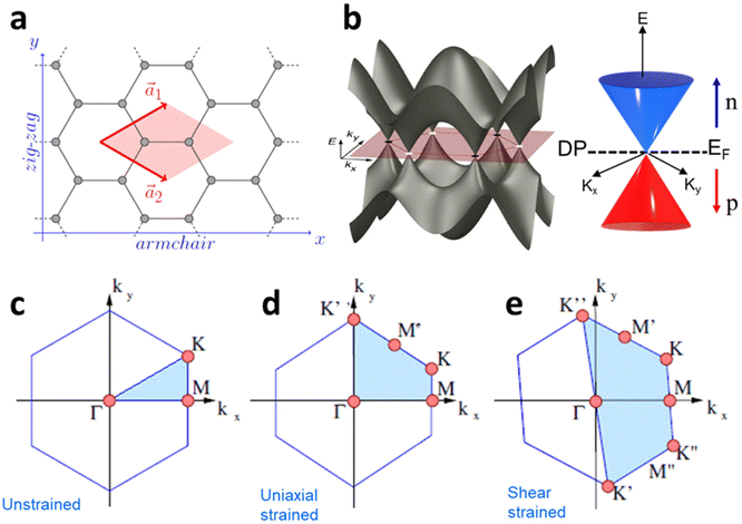 |
| | Fig. 1 (a) Hexagonal arrangement of carbon atoms in graphene, with vector basis  and and  . The shaded area represents the unit cell. The inequal crystallographic direction armchair along x-axis and zigzag along y-axis. (b) The high-symmetry (K) points of the hexagonal Brillouin zone (G, M, K) with a representation of characteristic linear bands intersecting at the Dirac point (DP) overlapped with Fermi energy level (EF) for unstrained and doped graphene. The shift of EF either to n or p leads to n-type and p-type doping respectively. Reprinted with permission from ref. 12 Copyright (2022) from IOP Publishing. (c–e) Illustration of BZ of graphene under strain. Reprinted with permission from ref. 20 Copyright (2022) from American Physical Society. . The shaded area represents the unit cell. The inequal crystallographic direction armchair along x-axis and zigzag along y-axis. (b) The high-symmetry (K) points of the hexagonal Brillouin zone (G, M, K) with a representation of characteristic linear bands intersecting at the Dirac point (DP) overlapped with Fermi energy level (EF) for unstrained and doped graphene. The shift of EF either to n or p leads to n-type and p-type doping respectively. Reprinted with permission from ref. 12 Copyright (2022) from IOP Publishing. (c–e) Illustration of BZ of graphene under strain. Reprinted with permission from ref. 20 Copyright (2022) from American Physical Society. | |
1.3. Influence of strain in MoS2
The physical distortion in MoS2 and other TMDs induces extrinsic disorder mostly after deposition over the substrate due to its intrinsic roughness and interfacial interaction such as ionic, covalent, electrovalent, van der Waals (vdW), etc.36 The roughness of the substrate is an inherent factor that inevitably leads to localised bending of the flexible 2D materials. Unlike the atomic layer of graphene, 1L MoS2 has three atomic layers (S–Mo–S) and exhibits a significant alternation in electronic structure that causes charge fluctuations during localised bending;23 see schematic in Fig. 2a and b. The electronic band structure dispersion over a supported substrate exhibits a deviation from its strain-free suspended membrane, where in the former, large broadening of electronic band structures along the energy axis has been observed.23 The local corrugation of MoS2 over silica substrate (i.e., vdW interaction) is reported to cause band gap (Eg) widening up to 2.65 eV without any aid of external straining. During the bent state, the spatial distribution of the S-atoms is altered. The atomic distances between the S-atoms increases in the inner (or outer) and decreases (or inner) in the sulphur layer; see Fig. 2c and d. The effect of these morphological corrugations is monitored through scanning tunnelling microscopy (STM) and correlated with localised variation with the Eg in Fig. 2d. It has been observed that there is a direct correlation with the conformation of MoS2 and its difference in the conduction band minimum (CBM) and valence band maximum (VBM) shows strain induced Eg modulation.13 The relation between the radius of curvature of the bent MoS2, induced strain and its variations in the Eg is illustrated in Fig. 2e, where a power law relationship is identified between band gap and radius of curvature, which is also related to the transformation of the direct to indirect band gap with increasing strain. This intrinsic corrugation-induced bending has converted 80% area of 1L MoS2 into the indirect band (around strain 1.5%) which is also reflected in the reduction of photoluminescence (PL) intensity. It has been observed that the strain values lying between 0.47–0.62% are responsible for the direct band gap, while 1.0–1.2% strain is responsible for indirect transition (Fig. 2f). The localised spatial distribution of indirect (dark blue colour) and direct (red colour) band gap along with local bending strain contour plot for MoS2-silica system is presented in Fig. 2g.13 The modulation of band gap due to physical strain is also regulated to texture designed surfaces. It has been observed that a strain up to 2.4% can alter the optical band gap around 108 meV.48 Over a textured surface such as nanocones, the externally induced strain can be reached up to 3% that leads to the band gap reduction up to 0.46 eV.49
 |
| | Fig. 2 Substrate induced strain in MoS2: (a) schematic illustration of 1L MoS2 with compressive and tensile strain. (b) Localised bending curvature from substrate roughness. (c) The conformation-induced bending curvature influences the separation distance between the inner and outer layers of sulphur atoms in atomic MoS2. (d) STM line profile of MoS2 topography and its associated band gap variations. (e) The relation between strain induced from morphology and radius of curvature of a bent MoS2 with band gap. (f) Transformation of direct to indirect transition band gap at different strain values. Reprinted with permission from ref. 13 Copyright (2022) from John Wiley and Sons. (g) Spatial distribution of localised region showing indirect and direct transition of the band gap. Reprinted with permission from ref. 23 Copyright (2022) from Springer Nature. | |
1.4. Gate doping and chemical doping
In the modern-day electronics, it is imperative to understand the modulation in electronic properties of the material through external stimulating environment. The injection of the charge carriers, either electrons, holes or ions to 2D materials can be performed through an electric field, electrochemical doping or chemical treatment without altering the physical properties.10 Generally, the electric field doping is carried out through field effect transistors (FET) with changing conducting channels between the mounted 2D material and applied gate voltage (Vg). A positive Vg injects electrons, while negative Vg induces higher density of holes in the 2D material, consequently altering the electric current. The relation between the surface charge density n and applied voltage Vg is illustrated in eqn (1):| |  | (1) |
where, ε0 and ε are the permittivity of free space and the supported substrate respectively, t is the thickness of the supported substrate oxide layer (e.g., silica), and e is the electron charge. The coefficient of the surface charge density induced by field effect, n/Vg, is estimated as 7.2 × 1010 cm−2 V−1. The change in carrier concentration shifts the Fermi energy (EF) of the 2D material accordingly. For monocrystalline graphene, EF of holes and electrons has been observed to be directly proportional to their concentrations (EF ∝ n), which is qualitatively different to its 3D bulk structure (EF ∝ n2/3).50 Under pristine conditions, graphene conductivity (σ) also increases linearly with Vg for both injections of electrons and hole carriers. The carrier mobility (μ = σ/ne) has been measured up to 15000 cm2 V−1 s−1 for both carriers independent of temperature range between 10–100 K.16
The electronic doping of graphene can also be carried out through adsorbate deposition of different electron affinities. Surface dopant with higher work function than the host material, such as metal oxides and oxidising gases (e.g., MoO3, NO2), causes p-type doping, while the surface dopant of lower work function, named as alkali metals and gases rich in electron pair (e.g., NH3), are responsible for the donation of electrons and causes n-doping. This phenomenon at the molecular scale can be explained through direct surface charge exchange across the electrochemical potential gradient at the interface between the 2D materials and surface dopant, which corresponds to the relative position of graphene EF and the molecular orbital level of surface dopants. If graphene EF is higher than the energy level of lowest unoccupied molecular orbital (LUMO) of an adsorbate, the electron will flow from graphene to the adsorbate, making graphene p-type doped. If the EF of graphene is lower than the level of highest unoccupied molecular orbital (HOMO), graphene gains the electron and becomes n-type doped (Fig. 3a).3 In semiconductors (e.g., metal dichalcogenides) with finite Eg, the energy level of valence band, conduction band and EF relative to LUMO/HOMO of the adsorbate molecule determine the type of doping to reach thermal equilibrium. If VBM of the semiconductor lies above the lowest level of LUMO, the electron will be transferred from the valence band to the adsorbate during contact. This charge migration changes the electron density at the interfaces which lead to band bending in upward direction and hole accumulation at the semiconductor, causing p-type doping. Nevertheless, if the CBM of the semiconductor lies slightly lower than the highest occupied HOMO level before contact, the electron will transfer from HOMO of the adsorbate to the conduction band of the semiconductor. It causes downward band bending and higher accumulation of the electrons in the semiconductor (n-type doping) until the stage of thermal equilibrium is reached (Fig. 3b).
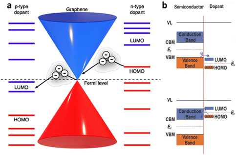 |
| | Fig. 3 Charge transfer mechanism between 2D materials and surface dopant: (a) schematic diagram of the energy bands of graphene with different electron affinities of the dopant. Reprinted with permission from ref. 3 Copyright (2022) from Beilstein Journal of Nanotechnology. (b) Schematic band diagram of the semiconductor based 2D materials towards surface dopants. Reprinted with permission from ref. 17 Copyright (2022) from John Wiley and Sons. | |
1.5. Influence of doping on conductivity
The electrical doping, either by electric field or surface adsorbate leads to alteration in current. Quantitively, the electrical conductivity σ and carrier concentration n can be related by σ ∝ na, where a < 1 for charge impurities and a > 1 for structural distortion such as ripples. Fig. 4a–c shows an example of graphene-based FET device demonstrating the change in conductivity from its pristine state to adsorbed impurities (K-atoms and NO2 gases) for different concentrations. It has been observed that the minimum conductivity with increasing the concentration of impurities (such as potassium atoms) saturates to a constant value around 4e2/h (for h as Planck constant) for graphene.2 Also, it leads to shifts in minimum Vg and is responsible for the asymmetry in the conductive curves for different polarities due to the change in the dopant concentration. The slope of the conductivity curve σ(Vg) unravels the measure of impurity scattering (so called field-effect mobility; μ = Δσ/Δne). Thus, the deviation in the slope values indicates that the doping from the impurities influences the scattering rate as observed in Fig. 4b for K-atoms and in Fig. 4c for NO2 adsorption.
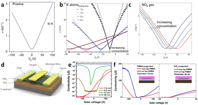 |
| | Fig. 4 Ambipolar transfer characteristics at different gate voltage (Vg) for (a) pristine graphene,2 (b) potassium adsorbed graphene at different concentration added at different time interval16 and (c) NO2 doped graphene at different concentration.27 Reprinted with permission from ref. 2, 16 and 27 Copyright (2022) from Springer Nature. (d) Schematic set-up of MoS2 FET with top gate (dielectric). (e) Conductivity of MoS2 as function of thickness from unipolar to ambipolar. (f) Conductivity of MoS2 at different substrates (SiO2 and PMMA). Reprinted with permission from ref. 33 Copyright (2022) from AIP Publishing. | |
Unlike graphene as zero-gap semi-metal, single layer of TMD, such as molybdenum disulphide (MoS2), have a wide band gap (Eg ≫ 1.8 eV) which is useful for monitoring electronic doping with reasonable high mobilities ∼217 cm2 V−1 s−1 (and >500 cm2 V−1 s−1 for bulk).51 The mobility of MoS2 varies with its thickness, which is related to the long-range dielectric effect and the dominance of long-range disorder that minimises the scattering of charges (Fig. 4d and e). The mobility of the charges in MoS2 can also be modulated through the addition of the superstrate (sometimes top gate) with highly dielectric materials (HfO2, ZrO2 PMMA) (Fig. 4f).33 The variation in the Eg of MoS2 with the thickness (Fig. 4e) makes it interesting for nanoelectronics applications to replace silicon in complementary metal–oxide–semiconductor (CMOS) logic devices. It is ideal for a semiconductor with Eg > 0.4 eV to have a current on/off ratio (Ion/Ioff) in the range between 104 and 107. While this value is limited in pristine graphene,52 the single crystal of MoS2 has demonstrated Ion/Ioff > 106 at an applied voltage of ±4 V comparable to silicon films.53 As shown in Fig. 4e and f, the conductivity of MoS2 varies with thickness and the nature of substrate; thinner layer (bi-layer) shows the n-type unipolar behaviour mostly over the SiO2 substrates. Nevertheless, MoS2 displays ambipolar behaviour around 6 layers with lower mobility of holes than electrons. At bulk state (>50 nm), major carrier of holes has been reported, indicating the p-type operation, which is suitable for FET and sensing applications.33 At similar thickness, dielectric polymeric support leads to the ambipolar trend in the conductivity, compared to unipolar trend over the SiO2 substrates with lower mobility. It has been argued that the presence of short-range disorder, chemical interaction with silica, or interface roughness scattering play important roles to bring down the conductivity.33
1.6. Measuring doping through Raman spectroscopy
Raman spectroscopy is a non-destructive optical characterisation technique sensitive to changes in the lattice structure, the electronic states, and the energy band of several 2D materials. The Raman active modes of the 2D materials are strongly related to the coupling between electrons and phonons (Fig. 5a and b).17 A shift in peak position (ωG) in the Raman active peak from its charge neutral state indicates the altering conditions of carrier concentration. In graphene, the extra charge carriers residing in honeycomb lattice structure lead to dynamical perturbation of G mode (∼1580 cm−1) lattice vibration. During the Raman scattering process, there is a creation and annihilation of long-wavelength virtual electron–hole pair across the Dirac point.54 The energy range of the virtual electron–hole pairs are regulated through Pauli principle, which is decided by EF level. In undoped graphene, the onset energy (ħωG) is considered zero. Under doped conditions, the increase/decrease in the carrier concentration improves the onset energy for vertical transition of an electron from a π valence band to a π* conduction band state to create virtual electron–hole pairs to 2EF (under the limitation of Pauli principle). Thus, the rise/fall of onset energy conditions leads to upshift/downshift of the G mode of graphene.17 At variable Vg, it has been observed G-peak position shift is minimum at the DP, indicating blue shift (stiffening) in G-peak position for both polarities. It is anticipated that the stiffening of the G mode is due to non-adiabatic removal of Kohn anomaly, which is usually responsible for phonon softening in graphitic materials under the condition of strong electron–phonon interaction.55
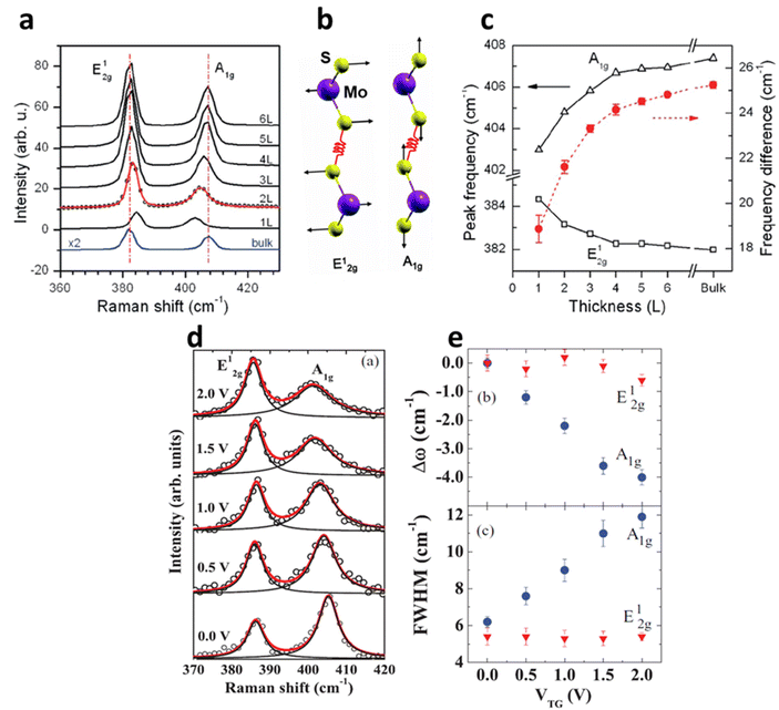 |
| | Fig. 5 (a) Raman spectrum of MoS2 at a different number of layers. (b) The schematic illustration of S and Mo atoms vibrations for E12g and A1g phonon modes. Reprinted with permission from ref. 1 Copyright (2022) from American Physical Society. (c) The shift in the Raman modes of MoS2 at different thicknesses. Reprinted with permission from ref. 15 Copyright (2022) from American Chemical Society. (d) The shift in the Raman modes and its broadening of 1L MoS2 at different top-gate voltages (V). The Raman peaks are fitted with Lorentzian line fit to monitor the peak shift and its broadening. (e) The shift in peak positions (Dω) and peak width (FWHM) of E12g and A1g at the gate voltage range 0–2 V. Reprinted with permission from ref. 28 Copyright (2022) from American Physical Society. | |
Also, the width of G phonon (GG) modes responds complimentarily to the stiffening of G mode. Yan and co-workers21 observed the Vg dependence for both ωG and GG that exhibit symmetrical changes at Vg = 18 V (Fig. 5c). A similar trend has also been demonstrated by Das et al.10 at Vg = 0.6 V which is directly related to the band structure of graphene as shown in Fig. 5d. The reduction in the GG (15 cm−1 to 6.5 cm−1) with increasing |Vg − VDP| indicates longer phonon lifetime relating to electron and hole concentration. This trend has been understood as Landau damping of phonons at higher carrier concentration in which the mode decays into particle–hole pair.21 At the 2D Raman modes (∼2700 cm−1) of graphene, the photoexcited electron emits an A1g phonon and the valley changes from K to K′ due to conservation of momentum. The effect of electronic doping of 2D Raman mode is different from G mode that electronic doping over 2D has minimal effect until a certain carrier concentration (∼3 × 1013 cm−2) is achieved through the polymeric ionic layer at ∼3 V. At higher Vg there is a redshift (softening), while for the hole doping there is a blue shift (Fig. 5e and f).17
Raman spectroscopy of semiconducting TMDs is also influenced by carrier doping determined by phonon characteristics. In MoS2, the evolution of the zone centre of E12g and A1g is due to lateral displacement of Mo–S atoms in the basal plane and atomic sulphur vibration along the c-axis respectively (Fig. 6a and b). The layer dependent Raman studies of MoS2 have shown the decrease in E12g frequency and increase in A1g phonons with increasing thickness (Fig. 6c). This opposite trend of E12g reflects the stacking induced structural change in the MoS2, and its anomalous phenomenon is attributed to enhanced dielectric screening of long-range Coulomb interaction between the effective charges at higher thickness.1 In 1L MoS2, increasing concentration of electrons occupies the bottom of the conduction band at K point, which has the characteristics of dz2 of Mo.28 This occupancy of the antibonding state in the conduction band enhances the total electronic energy of the system, resulting in weaker Mo–S bonds and phonon softening of A1g (red shift up to 4 cm−1) Raman mode as illustrated in Fig. 6d and e. The out-of-plane A1g Raman mode preserves the symmetry of the system and has strong electron phonon coupling than E12g, which explains the minor alteration (0.6 cm−1) of E12g under biasing conditions. Similarly, GA1g increases up to 6 cm−1 while GE12g remains insensitive. The phonon softening of A1g MoS2 at higher electron concentration has a distinctive trend than phonon hardening in graphene, as the latter blocks the generation of phonon induced electron–hole pair. Nevertheless, having a finite Eg, MoS2 shows different responses at various laser energy, especially at resonance excitation of laser energy used in the investigation.56–58
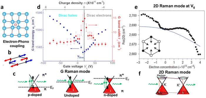 |
| | Fig. 6 Raman scattering of graphene: (a) schematic diagram of electron–phonon coupling. (b) G-phonon mode of vibrating carbon atoms. (c) Effect of G-peak position (ωG) and G-peak width GG at different Vg. Reprinted with permission from ref. 10 Copyright (2022) from Springer Nature. (d) Shift in 2D peak position ωG at different carrier concentration induced from different Vg, inset showing the schematic diagram vibration of carbon bonds in 2D Raman mode. Reprinted with permission from ref. 21 Copyright (2022) from American Physical Society. (e) Schematic of a Raman process in Dirac cones of graphene G Raman mode and (f) 2D Raman mode. Reprinted with permission from ref. 17 Copyright (2022) from John Wiley and Sons. | |
2. Deconvolution of strain and doping of 2D materials
2.1. Construction of strain and doping correlation
Unlike textured surfaces that induce static straining, soft surfaces such as polymeric materials allow dynamic strain and doping in 2D materials. Since Mohiuddin et al.8 first reported the G and 2D peak position shifts due to applied uniaxial strain, comprehensive studies on Raman spectroscopy of graphene in response to mechanical stimulus had been carried out.47 It is observed that the compression (tension) of the lattice reduces (increases) the interatomic distances and in turn leads to the redistribution of electronic charges, which upshifts (downshifts) the vibrational Raman modes.47,59 Consider a general strain tensor| |  | (2) |
where superscripts l and t represent the strain components in longitudinal and transverse directions, respectively. The rate of hydrostatic strain (εh = εll + εtt) of Raman mode i (G or 2D) can be related by Grüneisen parameter as:8,47| |  | (3) |
where ωi is the Raman peak position, ω0i is the strain-free Raman peak position, and γi is the Grüneisen parameter of the corresponding Raman mode. For an applied uniaxial strain εuni, the G peak splits into G+ and G− due to the non-zero shear component of the strain (εll ≠ εtt), while 2D peak does not split as it is associated with phonons at K point.60,61 Given that εll = εuni and εtt = −νεuni where ν is the Poisson's ratio of graphene, the Grüneisen parameter can then be expressed by:| |  | (4) |
| |  | (5) |
where Δω is the Raman shift deviated from the no-strain point ω0. When studying interactions between graphene and other 2D materials, however, biaxial strain εbi is usually involved.14 In such case, εll = εtt = εbi and G peak no longer splits due to the cancellation of shear deformation components; hence eqn (3) can be rewritten as:| |  | (6) |
or,
By applying the experimentally or theoretically determined value of γi,8,62,63 one can deduce the strain distribution of graphene through Raman shifts measurement. At low strain regime (ε < 0.5%), the phonon frequencies of both G and 2D vary linearly with strain.8 Hence, γi is a defined constant which will be useful in the construction of a correlation plot that will be discussed in later sections.
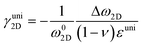
Raman modes of graphene are also susceptible to carrier concentration n due to the modification of electron–phonon coupling,10,64 which is generalised in Fig. 7a following results from Das and coworkers.10 Both p-doping and n-doping upshift G mode owing to the removal of the Kohn anomalies at Γ point,55 while an increase in carrier concentration (higher n-doping or less p-doping) always downshifts 2D mode due to the electronic transition of the energy of the phonons in double-resonant scattering.10,54 As pristine graphene and hybrid systems thereof are usually p-doped,35,65–67 it is expected the coordinates of Raman peak positions of unstrained graphene lie on the green coloured line in Fig. 7a. Low p-doping level (−1.0 × 1013 cm−2 < n < 0) can be well approximated by a first-order polynomial in terms of G or 2D peak position; it is thus possible to introduce a doping coefficient ki that:
 |
| | Fig. 7 Illustration of strain and doping correlation plot (Pos G vs. Pos 2D) of (a) graphene for both p- and n-doping, (b) graphene for only p-doping, and (c) MoS2. Each Raman dataset in G-2D axes represent the corresponding strain and doping in ε–n axes. | |
As ki is already known from Fig. 7a, the carrier concentration of graphene can be computed by measuring its Raman shifts. The interaction between graphene and other 2D materials often leads to both mechanical and electrical modulation, and this combined effect of strain and doping on Raman shift can be formulated by summing up eqn (7) and (8):
Lee and co-workers67 were the first to separate the effect of strain and doping by noticing that ε and n are linearly independent. By keeping other external effects constant such as single calibrated laser wavelength for dispersive Raman modes (e.g. D and 2D modes in graphene) and constant low laser power to avoid laser-induced temperature change throughout different measurements,68 ΔωG − Δω2D space can be regarded as a linear transformation of ε–n space, and each coordinate of Raman peak position represent a unique strain and doping configuration, i.e.,
| |  | (10) |
where
| |  | (11) |
In graphene system, ω1 and ω2 correspond to G and 2D modes respectively. A correlation plot can therefore be drawn in Fig. 7b with contour lines representing isostrain and isodoping. The value of strain and doping can then be evaluated by an inverse transformation:
| |  | (12) |
Using this equation, we can measure two Raman shifts, G and 2D for graphene, to determine two quantities of strain and doping. The sets of eqn (7)–(12) are not only applicable to graphene, but also to other 2D materials, such as MoS2, where subscripts (1) and (2) represent E12g and A1g modes respectively.69 Straining MoS2 leads to the modification of carrier effective masses and band gap energy,48,70 which consequently shifts the phonon frequencies of E12g and A1g modes. On the other hand, doping MoS2 results in the occupation of antibonding states at the K point,28,69 which results in downshifts of both E12g and A1g modes. Therefore, with Grüneisen parameters γi and doping coefficients ki of E12g and A1g modes known, we can also construct an analogous correlation plot of MoS2 to decouple strain and doping (Fig. 7c).
2.2. Determination of Grüneisen parameters and doping coefficients of 2D materials
Grüneisen parameters of graphene can be characterised either experimentally or theoretically by various techniques. At uniaxial strain, a typical method would be depositing graphene on a flexible substrate such as polyethylene terephthalate (PET) and bending the substrate (Fig. 8a).8 Assuming graphene is adhered to the substrate, this induces strain on graphene, which leads to Raman peak shifting (Fig. 8b). Grüneisen parameters can then be deduced by linear fitting of peak positions using eqn 4 and 5. Alternatively, pressure-induced compressive strain leading to shifts of graphene Raman peaks also enables the calculation of Grüneisen parameters.71 Several empirical methods for Grüneisen parameters at biaxial strain have also been developed, including piezoelectric actuator,72 nanobubble curvature,73 shallow depression on patterned SiO2,74 and recently, substrate-induced strain by thermal expansion coefficient (TEC) mismatch.75 Theoretically, Grüneisen parameters can also be deduced by DFT and first-principles calculations,8 which agree well with experimental values. Similarly, Grüneisen parameters of TMDs at uniaxial strain are measured by depositing it on polymers with subsequent bending48,70 as well as density functional theory with first-principles calculations.76 Michail et al.22 lately introduced in situ determination of Grüneisen parameters of MoS2 at biaxial strain using flexible cruciform substrate (Fig. 8c) backed by DFT calculations, which is essential for the evaluation of localised strain in 2D materials. Values of the above parameters of graphene and MoS2 are listed in Tables 1 and 2 respectively.
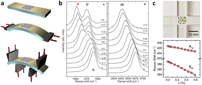 |
| | Fig. 8 Determination of Grüneisen parameters: (a) Schematic diagram of bending of graphene on PET substrate and (b) the corresponding Raman shift with increasing tensile strain. Reprinted with permission from ref. 8 Copyright (2022) from American Physical Society. (c) Illustration of MoS2 bending measurement and its influence on Raman shift. Reprinted with permission from ref. 22 Copyright (2022) from IOP Publishing. | |
Table 1 Determination of Grüneisen parameters of graphene
|
γ
G
|
γ
2D
|
Strain |
Method |
Ref. |
| 1.99 |
2.7 |
Uniaxial |
Experimental |
71
|
| 1.99 |
3.55 |
Uniaxial |
Experimental |
8
|
| 1.87 |
2.7 |
Uniaxial |
Theoretical |
8
|
| 1.8 |
2.6 |
Biaxial |
Experimental |
73
|
| 1.8 |
2.8 |
Biaxial |
Experimental |
72
|
| 1.95 |
3.15 |
Biaxial |
Experimental |
75
|
| 2.4 |
3.8 |
Biaxial |
Experimental |
74
|
| 1.8 |
2.7 |
Biaxial |
Theoretical |
8
|
Table 2 Determination of Grüneisen parameters of MoS2
|
γ
E2G1
|
γ
A1G
|
Strain |
Method |
Ref. |
| 0.6 |
0 |
Uniaxial |
Experimental |
70
|
| 1.1 |
0 |
Uniaxial |
Experimental |
48
|
| 0.65 |
0.21 |
Uniaxial |
Theoretical |
76
|
| |
| 0.6 |
0.22 |
Biaxial |
Experimental |
22
|
| 0.56 |
0.13 |
Biaxial |
Theoretical |
22
|
Measurement of doping coefficients can be obtained directly by electronic top-gated field-effect transistor10,28 discussed in the previous section. An applied top-gated voltage contributes to a change in the doping concentration of 2D materials, which can be monitored by Raman spectroscopy. Generally accepted values of doping coefficients are respectively kG = −1.407 × 10⁻¹² cm−1, k2D = −0.285 × 10⁻¹² cm−1,10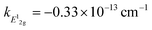 and kA1g = −2.22 × 10⁻¹³ cm−1.28
3. Applications of strain and doping model
While the evaluation of strain and doping is first used to understand the mechanisms in thermal annealing of graphene,7,67 it could also be used for studying intrinsic mechanical and electronic properties of pristine 2D materials such as the contribution of strain and doping by structural defects,14 the interaction of two layered materials in vertical heterostructure,4,5,9,77 corrosion in 2D material covered metal surfaces37 and textured surfaces,11 and the temperature-dependent strain and doping measurements.6,78,79 The above applications will be discussed individually in the following section.
3.1. Thermal annealing of graphene
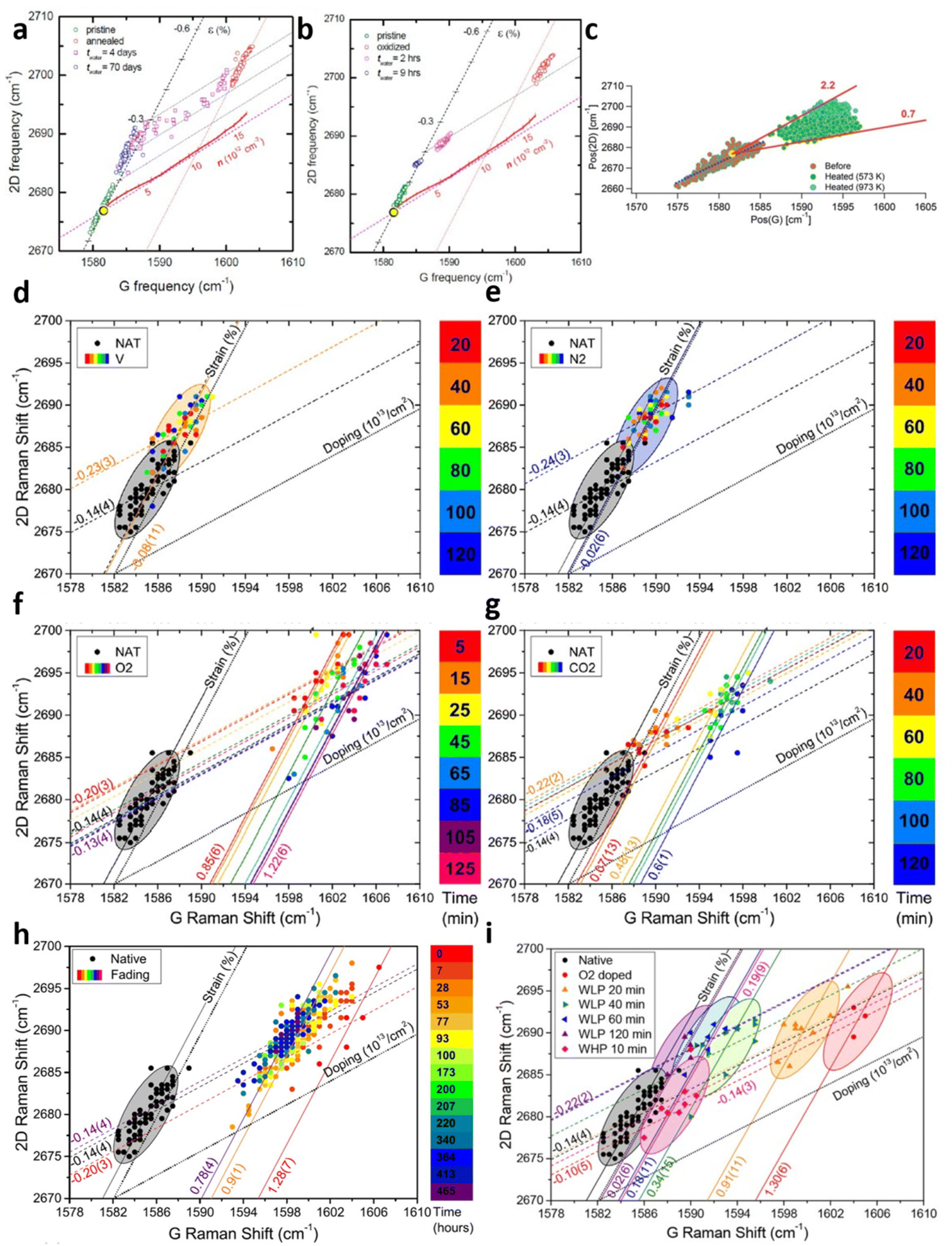
While Lee et al.67 demonstrated the modulation of compressive strain and hole doping due to thermal annealing of graphene on silica (Gr/SiO2), the research continued to explore the origin of the phenomenon and its reversibility as shown in Fig. 9a.7 The annealing of Gr/SiO2 leads to compressive strain of 0.28%, which can be attributed to the lattice contraction. Given the negative thermal expansion coefficient (TEC) of graphene compared to the positive one of silica,14,80 the expansion of graphene and the shrinking of underlying silica result in compressive strain of graphene during the cooling process.81 Thermal annealing also reduces the electron concentration by 1 × 1013 cm−2 because of oxygen-mediated hole doping.65 As for reversibility, water immersion counters the doping effect where the carrier concentration returns to the pristine undoped stage. Considering no further change in strain or doping after drying in ambient conditions,7 it is shown that doping by thermal annealing is reversible by water immersion. The in situ measurement illustrates the edge of the graphene flake is quicker to achieve this water-induced recovery than the central region (i.e., basal plane),7 suggesting the p-doping by annealing may be due to trapped oxygen beneath Gr/SiO265 that the intercalation of water between Gr/SiO2 interface leads to the replacement of oxygen molecules by water and thus the prohibition of oxygen-mediated hole doping. This speculation is supported by a separate measurement7 where graphene is oxidised to form nanopores throughout the layer with subsequent annealing and immersion in water as shown in Fig. 9b. The shorter time required for the doping level to return to the pristine one, as well as the similar recovery speed between the edge and the inner region7 suggests the nanopores provide additional intercalation channel to enable water diffusion to the Gr/SiO2 interface.
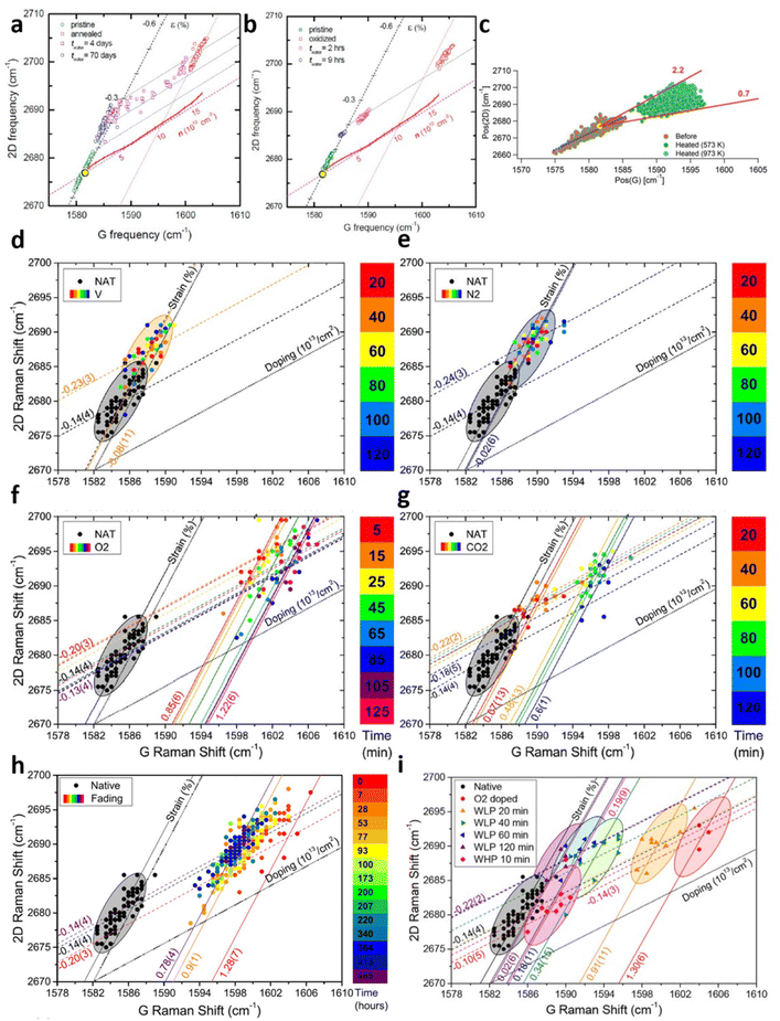 |
| | Fig. 9 Strain and doping evaluation in graphene annealing: (a) annealing effect and its water-induced recovery for pristine Gr/SiO2 and (b) oxidised Gr/SiO2. Reprinted with permission from ref. 7 Copyright (2022) from American Chemical Society. (c) Annealing effect at different elevated temperatures. Reprinted with permission from ref. 18 Copyright (2022) from RSC Publishing. (d) Annealing effect under vacuum, (e) nitrogen, (f) oxygen, and (g) carbon dioxide over time. NAT corresponds to native Gr/SiO2. (h) De-doping effect of annealed graphene in air and (i) water over time. Reprinted with permission from ref. 29 Copyright (2022) from Elsevier. | |
Graphene annealing can be further studied by tuning the annealing temperature as well as re-annealing with the help of in situ Raman spectroscopy, as depicted in Fig. 9c.18 Cooled Gr/SiO2 after thermal annealing at 573 K shows a compressive strain of 0.13% and hole doping of 1.1 × 1013 cm−2, agreeing well with previous experimental studies.7,67 Higher annealing temperature at 973 K allows the compressive strain continues to develop but the doping level remains comparable. This result supports the earlier explanation that higher temperature culminates in a stronger lattice contraction effect while the oxygen-mediated p-doping has already taken place at low temperature and hence a higher temperature no longer strengthens the hole doping. It is also suggested that thermal annealing leads to closer contact between graphene layer and silica which increases the p-doping of graphene. While the air exposure of first-time annealed Gr/SiO2 does not shift the Raman modes back to the pristine stage, real-time re-annealing studies18 show that this Raman shifting is reversible starting from the second annealing cycle (compared to annealed graphene). This can be attributed to the carbon–carbon bond and phonon interactions that the irreversible changes (such as oxygen-mediated doping and changes in contact between graphene and substrate) are completed.
A comprehensive study of thermal annealing in graphene was carried out by Armano et al.29 by heating Gr/SiO2 under different gases, including vacuum, nitrogen, oxygen, and carbon dioxide with increasing number of time intervals as shown in Fig. 9d–g respectively. Pristine Gr/SiO2 has an intrinsic compressive strain of 0.14% with negligible doping during the CVD fabrication. In vacuum and nitrogen environments, thermal treatment increases the compressive strain to 0.23% and 0.24% respectively but does not dope the sample. This effect is already observed in the first 20 minutes while longer treatment does not undergo any further modification. Thermal annealing under oxygen and carbon dioxide also leads to comparable compressive strain of 0.20% and 0.22%; however, significant p-doping occurs, reaching up to 1.22 × 1013 cm−2 and 0.6 × 1013 cm−2 respectively. It is worthy to note that with increasing heating time, oxygen mediated p-doping takes place in two steps: a fast and substantial hole doping (0 → 0.85 × 1013 cm−2, 0 → 5 min) followed by a slow and lesser hole doping (0.85 × 1013 cm−2 → 1.22 × 1013 cm−2, 5 → 125 min). These two processes may be either the adsorption of oxygen molecules to graphene at the basal plane,82,83 or oxygen and water involved electron transfer in a redox reaction.84,85 In contrast, the compressive strain is reduced back to the pristine stage with further temporal steps (>100 minutes), which may be associated with the softening in mechanical interaction by the intercalation of water molecules in Gr/SiO2 interface.29 As for the reversibility, the effect of air exposure is shown in Fig. 9h that graphene is de-doped from 1.28 × 1013 cm−2 to 0.78 × 1013 cm−2 after 465 hours in air. This de-doping process also occurs in two steps that the fading mainly takes place in the first 7 hours of air exposure. It is thus possible to interpret these results as two doping (and de-doping) stages. The fast and substantial doping and slow de-doping of 0.9 × 1013 cm−2 can be attributed to a low activation barrier and a deep energy trap which is probably due to the adsorption of oxygen molecules beneath graphene. Low activation barrier is due to minimal charge transfer in adsorption86 while deep energy trap can be explained by the localisation of oxygen molecules on the Gr/SiO2 interface protected from atmosphere by graphene, i.e., oxygen molecules between graphene and silica inducing p-doping cannot be reached easily by air.69,82,83,87 The slow doping and fast de-doping of 0.4 × 1013 cm−2 can be correlated to high activation energy and shallow energy trap which is probably due to electron transfer in redox reaction, as redox reaction needs a high energy barrier while large interaction of charges with atmosphere provides a low energy trap.84,85 This theory can be further supported by in situ water immersion measurement in Fig. 9i. While the doping level of graphene is reduced by 0.4 × 1013 cm−2 in the first 20 min, corresponding to the second stage and is comparable to the air exposure environment, it continues to slowly drop to the pristine level associated to the first stage unlike air treatment, which is due to the ability of water diffusing across the graphene to remove the oxygen molecules on the Gr/SiO2 interface.7 With the help of strain and doping model, the mechanics of thermal annealing of graphene and its reversibility are extensively explored.
3.2. Modulation of strain and doping by structural defects and textured surfaces
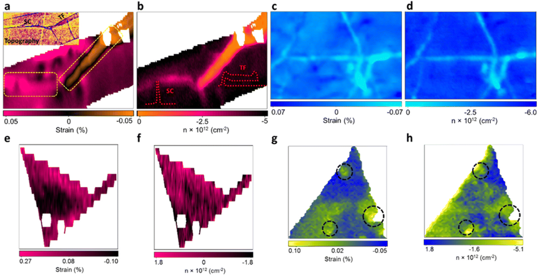
With the benefit of the deconvolution model, the variation of strain and doping in pristine 2D materials culminated from structural defects in the manufacturing process were studied by Tripathi et al.14 Combining the model with atomic force microscopy (AFM) enables the identification and measurement of common structural defects in different materials with different fabrication methods, including mechanically exfoliated (ME) graphene (Fig. 10a and b), chemical vapor deposited (CVD) graphene (Fig. 10c and d), ME MoS2 (Fig. 10d and e), and CVD MoS2 (Fig. 10f and g). In ME graphene, wrinkles are one of the common line defects arising from the balance between adhesion energy and bending energy during the transfer process.88,89 Surprisingly, wrinkles with opposite influences to mechanical strain are recognised, which can be attributed to two different buckling orientations:90,91 Small ripples with a height less than 8 nm tend to remain upright to form standing collapsed (SC) wrinkles as illustrated in the inset of Fig. 10b, which correspond to a tensile strain (or release of compressive strain from surrounded basal plane) up to 0.5%. After exceeding this critical height, the excess bending energy leads to the bending of ripples towards the substrate which are referred as the transitional-folded (TF) wrinkles (Fig. 10b inset) and a compressive strain up to 0.5% is induced. The electronic modulations from these two types of wrinkles are also different. As compared to the defect-free region where Gr/SiO2 is originally p-doped with a doping level of 4.2 × 1012 cm−2, SC wrinkles reduce the p-doping to 2.6 × 1012 cm−2 and TF wrinkles exhibit a stronger inhibition against p-doping to 1.1 × 1012 cm−2. This can be interpreted by the less coupling with the substrate in the buckled structure and the gap between graphene and silica is larger in TF than in SC wrinkles.14,92 It is worth noting that the spatial resolution of the Raman probe can be estimated between 200 and 400 nm, depending on the laser wavelength and objective used.14,93 While the resolution is usually larger than the defects, wrinkles, or sometimes the lateral size of the 2D materials, the influence of these effects can still be identified and resolved in the Raman signal. Due to small relative volumetric contribution, the scattering cross-section signals from the localised defects are weak, thus, individual point defects or vacancies in the nanoscale are challenging to be unambiguously characterised with Raman spectroscopy. Nonetheless, structural disorder such as wrinkles having smaller widths (10–40 nm) but larger lengths (few microns) can be well characterised by Raman spectroscopy. Several attempts have been taken to confine the laser into sub-diffraction limit and to enhance the scattering signals to the detectable level by generating a local plasmonics through localised light-metal interaction under surface-enhanced Raman spectroscopy (SERS) and tip-enhanced Raman spectroscopy (TERS) techniques.94 Wrinkles are also observed in CVD graphene (Fig. 10c and d) due to its lower TEC than that of substrate and thus the lattice mismatch during the cooling process in fabrication.80 A compressive strain up to 0.051% and a reduction of p-doping of 2.18 × 1012 cm−2 are measured in the wrinkles region, which is comparable to the TF wrinkles in ME graphene.
 |
| | Fig. 10 Strain and doping maps of structural defects: (a) strain map of ME graphene showing standing collapsed (SC) (left dashed rectangle) and transitional folded (TF) wrinkles (right dashed rectangle). Inset shows the AFM image of topography for the identification of wrinkles. (b) The corresponding doping map of the same region in (a). Inset shows the schematic appearance of SC and TF wrinkles. (c) Strain and (d) doping map of CVD graphene showing the wrinkles in light blue colour. (e) Strain and (f) doping map of ME MoS2 showing the inner defect free region (in black) and wrinkles near the edge (in pink). (g) Strain and (h) doping map of CVD MoS2 showing the pit-holes as indicated by dashed circles. Reprinted with permission from ref. 14 Copyright (2022) from American Chemical Society. | |
In ME MoS2 (Fig. 10e and f), while the defect-free centre region displays accumulation of compression strain ranging from 0.01% to 0.09%, the wrinkles near the edge release the intrinsic compressive strain into a tensile strain of 0.14 to 0.27%. An increase in electron concentration is also observed at the wrinkles region, suggesting the tensile strain in wrinkles be responsible for the increase in the mobility of the charge carrier.14,95 In CVD MoS2 (Fig. 10g and h), the defect-free region possesses a higher built-in tensile strain than ME system, which is due to the TEC mismatch between MoS2 and silica substrate.96 This tension on the basal plane also prevents the formation of wrinkles. Pit-holes, another structural defect, however, emerge from the etching of the silica substrate by alkali metal precursors in CVD fabrication97 and culminates in tensile strain varying from 0.01% to 0.07% with a wide range of modulation on doping. This can be attributed to the bending along the circular trench in pit-hole regions.14 The above results of doping in structural defects are in good agreement with separate Kelvin probe force microscopy (KPFM) measurements, suggesting the versatility for the strain and doping model. While the structural defects modulate the strain distribution, they are randomly spread over the surface which is difficult to regulate. Therefore, controlled strained and doped systems can be achieved through deposition of 2D material over periodic arrays or on textured surfaces, where the protruded surface induces local stretching and contraction of the flexible 2D material. The extent of strain depends on the aspect ratio (height or width/spacing between the protruded regions) of the textured surface and interfacial interactions.98 Recently, a systematic Si grooved surface of different pitch lengths (40 nm, 125 nm and 250 nm) at comparable depth has been investigated (Fig. 11a–c).11 The conformation of the graphene layer to each patterned surface induces different strain between crest and trough regions, which can be validated by Raman mapping through the deconvolution model (Fig. 11d). It has been observed that the flat Si surface induces compressive strain in the graphene which systematically decreases over textured surfaces with reducing pitch length. Such textured architectures were useful to study nanoscale cog of nanogears for the lubrication nanoscale devices. A similar work is presented by the deposition of graphene over silica nanospheres of different diameters, in which the optimised strain distribution around the spherical shaped was used to explore strain engineering in graphene.98
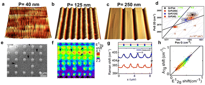 |
| | Fig. 11 Textured induced strain and doping in 2D materials: (a–c) 3D AFM images of graphene-covered Si textured surface of different pitch lengths: 40, 125, and 250 nm, respectively. (d) Correlation plot of graphene over different textured surfaces showing trend of strain and doping with various extent of conformation. Reprinted with permission from ref. 11 Copyright (2022) from John Wiley and Sons. (e) SEM (scanning electron microscopy) micrograph of MoS2-covered pillar-shaped structure. (f) Raman map showing the shift in E12g peak position over the pillar as compared to the flat surface. The marked arrows represent the Raman signal from ripples generated due to strain between two or more nanopillars. (g) Line profile from Raman spectroscopy showing distinguishable shift in Raman modes (E12g and A1g) of MoS2 between pillars and basal surface. (h) Correlation plot showing a trend in the Raman modes, and the solid line revealing the linear trend. Reprinted with permission from ref. 25 Copyright (2022) from American Chemical Society. | |
The optomechanical measurement using MoS2 has been carried out over Si/silica nanopillar arrays (height 420 nm and 820 nm) as shown in Fig. 11e.25 The strain in the suspended MoS2 is regulated by introducing a “tent” structure around the nanopillars. Raman measurements indicate the appearance of the highest strain at the centre of the pillar's apex (Fig. 11f). By monitoring the shift in E12g and A1g, a tensile strain of around 2% has been evaluated, which was claimed to be undervalued due to laser spot size restriction. The maximum strain was anticipated up to 2.4%. The contribution of doping has been determined by measuring the Raman line profile for peak shift in E12g and A1g. The results reveal that the modulation in A1g is more effective than E12g (up to 8.2 times) that depicts a strong doping-dependent signature (Fig. 11g). The correlation plot revealed a linear dependence with a slope of 1.1 indicating the influence of the electron–phonon interaction (Fig. 11h).25
3.3. Strain and doping in vertical heterostructure
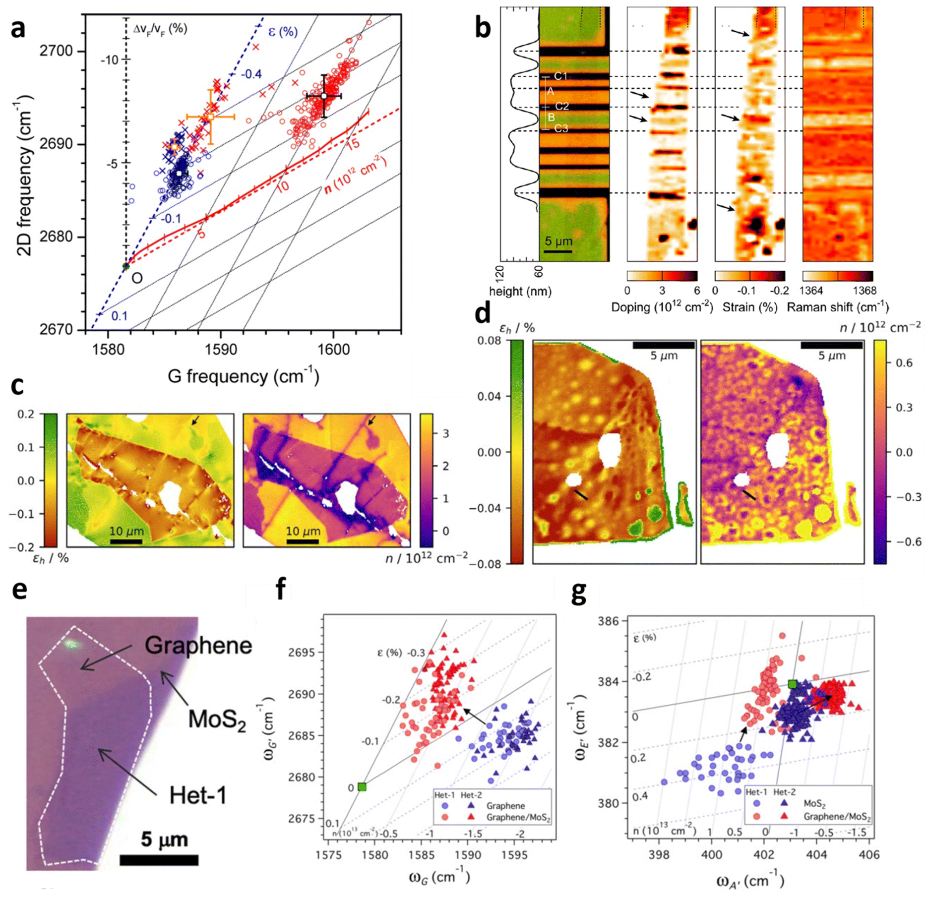
Vertical heterostructures of 2D materials have been used to exploit the synergy from individual layers for a range of applications. Graphene over hexagonal boron nitride (hBN) and MoS2 are among the common examples of vertical heterostructures. Given that hybrid architecture of Gr/hBN is related to field-effect tunnelling99 and Anderson localisation which results in metal–insulator transition,100,101 an investigation of the effect of beneath hBN to the top layer graphene is thus illustrated in Fig. 12a.9 By comparing Gr/hBN with Gr/SiO2 under ambient conditions, the doping from hBN to graphene is found to be insignificant, while hBN induces additional 0.1% compressive strain to graphene compared to Gr/SiO2. The thermal annealing at 673 K barely induces hole doping in Gr/hBN (3 × 1012 cm−2) which is less than that of Gr/SiO2 (1 × 1013 cm−2), possibly due to hydrophobic hBN attracting fewer water molecules in the interface for doping65,102,103 or the reduction in ripple formation in highly flat hBN.65,67,104
 |
| | Fig. 12 Interaction between graphene and hBN: (a) correlation plot of the hBN and annealing effect to graphene. Circles represents bare graphene and crosses represents Gr/hBN. Blue colour corresponds to before annealing and red colour corresponds to after annealing for 2 h at 673 K. Reprinted with permission from ref. 9 Copyright (2022) from American Chemical Society. (b) Left to right: false colour image for hBN/Gr on different substrate, doping map, strain map, and Raman shift. In false colour image, black represents hBN/Gr on MgO/Co electrode, green represents hBN/Gr on silica substrate, and orange corresponds to suspended hBN/Gr. Reprinted with permission from ref. 24 Copyright (2022) from American Chemical Society. (c) Strain and doping map of hBN/Gr/SiO2. hBN locates at the middle of the image while Gr/SiO2 substrate constitutes the background. (d) Strain and doping map of hBN/Gr/hBN. Reprinted with permission from ref. 31 Copyright (2022) from IOP Publishing. (e) Optical image of graphene over MoS2. (f) Correlation plot of Gr/MoS2 in the perspective of graphene and (g) MoS2. Circles and triangles correspond to different samples. Reprinted with permission from ref. 35 Copyright (2022) from American Physical Society. | |
The model can also be applied for the examination on an innovative graphene spin-valve device comprising of MgO/Co, SiO2, and hBN/Gr as depicted in Fig. 12b.24 In the device, hBN/Gr is partly suspended and partly supported on SiO2, and the strain and doping evaluation indicates slight doping (<5 × 1011 cm−2) in the suspended region but significant doping (3 × 1012 cm−2) in SiO2 supported region. The substantial doping may be due to vacancies or charged defects in MgO/Co electrodes as well as local electric field in SiO2.105,106 On the other hand, insignificant strain is observed in suspended region while compressive strain of 0.2% is measured at SiO2 supported region, which may arise from the bending of graphene or substrate-induced effect.67,107
Another inspection of strain and doping distribution was performed in hBN/Gr/SiO2 and hBN/Gr/hBN heterostructures as shown in Fig. 12c and d respectively.31 In the former hybrid, hBN induces compressive strain to graphene owing to the difference in TEC,108 leading to a transition of 0.5% tensile strain in bare graphene to 0.1% compressive strain in hBN-covered graphene region. hBN also results in a decrease in p-doping from 3 × 1012 cm−2 to 1 × 1012 cm−2 by shielding graphene from any environmental adsorbates.31 When graphene is sandwiched between two hBN flakes (Fig. 12d), the strain and doping distribution is less spread, implying the encapsulation provides an insulation from external factors causing the variation. The overall compressive strain of flat graphene is between 0.03% and 0.06%; however, in large bubbles, a tensile strain of 0.06% is induced. There are also small bubbles releasing the compressive strain of graphene to almost non-strained condition. The overall graphene is charge-neutral because of the hBN protection from adsorbates and the prohibition of doping from SiO2 substrate. Bubble regions, however, show a slight p-doping up to 0.6 × 1012 cm−2, which may be attributed to changes in Gr/hBN interaction near the cavity edge owing to interlayer separation or hBN edge potentials.109,110
Given that Gr/MoS2 heterostructure is of interest for applications including optoelectronics and photovoltaics,111–113 the deconvolution model allows the evaluation of induced strain and doping of both materials, which is extensively studied in Fig. 12e–g.35 While bare graphene is originally p-doped with doping level of 1.4 × 1013 cm−2 and experiences tension up to 0.3%, the embedding by MoS2 causes a reduction of p-doping to 0.4 × 1013 cm−2 and a transition from tensile to compressive strain up to 0.3% (Fig. 12f). The measurement on MoS2 Raman modes (Fig. 12g) reveals that MoS2 conversely becomes p-doped and undergoes a drop in tension (compression) in the presence of graphene. Both results demonstrate a donation of electrons from MoS2 to graphene which can be explained by electron-rich feature of MoS2 compared to electron-poor graphene. The induced strain can also be interpreted by different TEC between graphene and MoS2 which leads to lattice mismatch during the CVD process.4,62,114 To examine the possibility of modulation in strain or carrier concentration, both samples are annealed at 623 K in argon.35 Graphene is further p-doped and compressed after annealing, as expected due to the oxygen residue trapped in the interface and the lattice contraction.67,115 While this culminates in an absolute shift in strain and doping of both Gr and Gr/MoS2, the difference in strain and doping among them remains comparable, i.e., the thermal annealing does not alter the relative strain and doping in graphene due to the embedding of MoS2. This is also supported by a similar response in MoS2 annealing in argon35 that the strain and doping modulation are absolute but not relative.
3.4. Graphene on metal surfaces
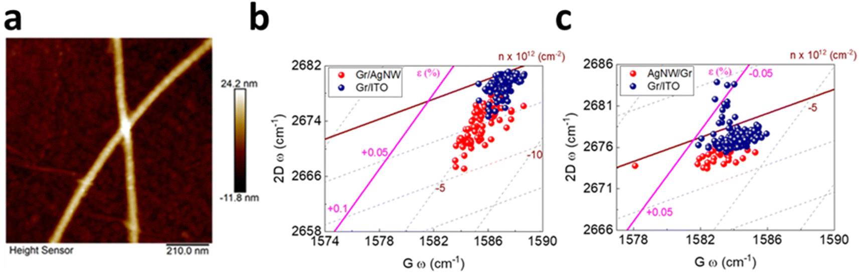
Hybrid between graphene and silver nanowire (AgNW) has recently attracted considerable interest in light of the conductivity enhancement in transparent electrodes as well as the improved performance of photovoltaic devices due to surface plasmon resonance.5,110,116 It is thus rational to study the induced strain and doping in the vertically stacked heterostructure in either Gr/AgNW (Fig. 13a and b) and AgNW/Gr (Fig. 13c) orientation.5 In the former system, the underneath AgNW does not lead to discernible doping but induces tensile strain up to 0.06% to the upper graphene layer, indicating the conformation of graphene by the AgNW. In latter (Fig. 13c), the topping of AgNW on graphene exhibits a similar response, albeit weaker, of negligible doping and 0.01% tensile strain. This can be inferred by a slight extension of carbon–carbon bonds as compared to Gr/ITO.5
 |
| | Fig. 13 (a) AFM image of graphene covered AgNW. (b) Correlation plot of Gr/AgNW and (c) AgNW/Gr heterostructure. Blue colour represents bare graphene while red colour represents incorporation of AgNW. Reprinted with permission from ref. 5 Copyright (2022) from MDPI. | |
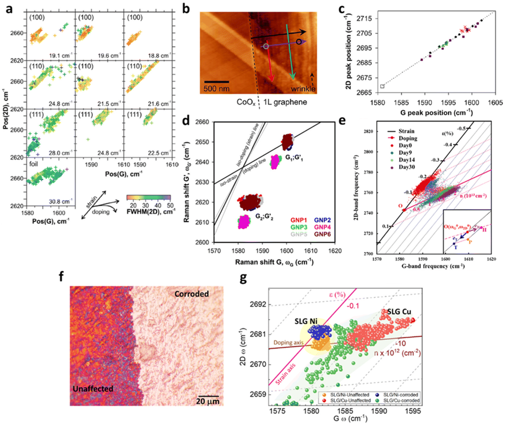
Given copper being the most widely employed substrate for CVD graphene fabrication,117 a detailed understanding of the interplay between the copper catalyst and graphene will thus be essential. The strain and doping evaluation serve as a powerful tool to investigate the effect of crystalline nature and the lattice orientation of copper on the graphene growth, which is illustrated in Fig. 14a.4 The magnitude of compressive strain induced on graphene is highly dependent on the lattice orientation of copper as the following order: Cu (111) > Cu (110) > Cu (100). The vector analysis reveals that Cu (111) induces an additional 0.2% compressive strain when compared to Cu (100), which may be due to the different mismatch between lattice parameter of copper and equilibrium C–C bond length during the formation of different superstructure of graphene at Cu (111) and Cu (100).4,118 This result agrees with a separate molecular dynamics simulation118 suggesting a higher compressive strain in Cu (111) than Cu (100).
 |
| | Fig. 14 Correlation plots of graphene on metal surfaces: (a) correlation plot of graphene on Cu with different lattice orientations including Cu (100), Cu (110) and Cu (111). Reprinted with permission from ref. 4 Copyright (2022) from Elsevier. (b) AFM image and (c) the correlation plot of graphene on Co. The colour of the arrows in the AFM image represents the data points in the correlation plot. Graphene near the edge (red) shows a larger compressive strain than graphene in the inner area (green). Reprinted with permission from ref. 19 Copyright (2022) from American Chemical Society. (d) Correlation plot of graphene on NPs. G1; G′1 corresponds to the flat region and G2; G′2 corresponds to wrinkled region. Reprinted with permission from ref. 30 Copyright (2022) from Springer Nature. (e) Correlation plot of graphene on Cu with time. Reprinted with permission from ref. 34 Copyright (2022) from American Chemical Society. (f) Optical image of graphene over Cu surface which is partially exposed to a strong acid (H2SO4), where both regions have been taken for the Raman analysis. (g) Correlation plot of graphene single layer (SLG) over Cu and Ni showing tension in the corroded region as compared to unaffected. Reprinted with permission from ref. 37 Copyright (2022) from American Chemical Society. | |
Formation of graphene wrinkles on metal surface also provides a magnificent example for the deconvolution model. As shown in Fig. 14b and c,19 the strain and doping distribution of Gr/Co wrinkles are studied. While minimal doping (a change of carrier concentration less than 1.3 × 1012 cm−2) takes place across the entire graphene sheet, compressive strain of 0.38% is induced at the supported region in Gr/Co, which can be attributed to the TEC difference that graphene expands when it is cooled during the fabrication process. A larger compressive strain is induced near the edge than the central region, and hence it can be speculated that the edge of graphene is pinned with the strongest compressive strain, which is gradually relieved along the inner region until wrinkles are generated where compressive strain is the lowest.119–122 A separate measurement19 indicates that compressive strain recovers in between wrinkles, leading to an intriguing phenomenon of ‘strain field’. A deliberate wrinkle generation can also be performed by depositing graphene on iron oxide nanoparticles (NPs) on SiO2 where the induced strain and doping are studied in Fig. 14d.30 Wrinkles are formed by the curvature of NPs and successfully located as G2; G′2 from the flat region (G1; G′1) corroborated from AFM results. In low wrinkling area, graphene is heavily p-doped (1.3 × 1013 cm−2) with insignificant strain which is due to large area coupling with the SiO2 substrate, while high wrinkling reduces the hole doping to 1.2 × 1013 cm−2 with 0.06% tensile strain due to less contact area with the substrate.30,123
The modulation of strain and doping in graphene by the morphology of metal substrate can also be realised by growing graphene on Cu where Cu gradually oxidises to form Cu2O as illustrated in Fig. 14e.34 Recent studies124–126 show that the attachment of water molecules to the structural defects of graphene such as wrinkles and grain boundaries leads to the oxidation of Cu to Cu2O. Between day 0 and day 9, graphene remains compressive (0.15%) with no doping (<1 × 1012 cm−2). With increasing oxidation of Cu beneath, the compressive strain is completely released to non-strained condition and becomes p-doped. On day 30 and onwards, tensile strain even develops in graphene and p-doping increases to 1 × 1013 cm−2. In situ measurement demonstrates this strain and doping effect is faster on defect sites such as wrinkles. The overall result can be explained as graphene initially possesses compressive strain due to lower TEC of graphene than Cu,4,19 the curvature by the oxidation of Cu into Cu2O particles releases the compressive strain.34 As Cu2O is a p-type semiconductor with a band gap of 2.17 eV,127 graphene is also gradually p-doped with time. As the defect sites provide more diffusion pathway for oxidation, accelerated tension generation and hole doping response at that area are recognised.
In addition to the nanoscopic investigation of graphene wrinkles, the chemical and physical changes in Cu foil by corrodents (H2SO4) are successfully identified by graphene through strain and doping at the micro scale.37 Partial surface of polycrystalline Cu exposed to the H2SO4 are physically etched the Gr/Cu surface (Fig. 14f) and affects the carrier concentration (Fig. 14g). By observing a similar phenomenon over graphene deposited on Ni surface, it is suggested that the presence of grain boundaries permeates the corrodents and etches the metal surfaces, causing tension in the graphene layer. Considering the grain boundaries as the weak centre of single layer graphene, multi-layered system has been implemented to protect the Cu surface from biotic and abiotic corrosion, which shows promising results. Thus, the topping of graphene layer can act as a corrosion sensing medium.
3.5. Temperature-dependent strain and doping
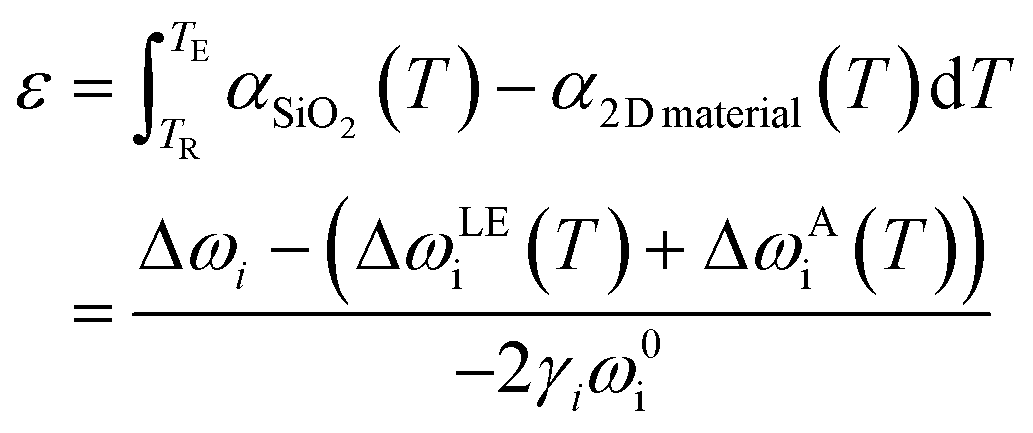
In situ Raman measurement at different temperatures can reveal crucial information of graphene and MoS2 such as TEC,78,80,128 thermal conductivity,129,130 and the strain and doping modulation by external heat.6,79 At elevated temperatures, strain and doping are no longer the exclusive factors for the shift of Raman modes; instead, the lattice expansion and anharmonic coupling also lead to the phonon shifts.130–132 The addition of these thermal influences to eqn (9) results in| | | Δωi = 2γiωi0ε + kin + ΔωiLE + ΔωiA | (13) |
where ΔωiLE and ΔωiA represent the lattice expansion and anharmonicity effect. The Δ sign means the change of the absolute thermal effect, ωiLE(T) and ωiA(T), at the elevated temperature TE from the reference temperature TR, i.e.,ΔωiLE + ΔωiA = ωiLE(TE) + ωiA(TE) − (ωiLE(TR) + ωiA(TR)). For graphene, this combined thermal effect ωiLE(T) + ωiA(T) has been extensively studied and the value can be approximated by a third-order polynomial.131,133 For MoS2, this term is reported to be linearly proportional to temperature and can be estimated by a first order polynomial.129,130 The general accepted values129,131,133 are therefore listed in eqn (14) and Table 3.| | | ωiLE(T) + ωiA(T) = c0 + c1T + c2T2 + c3T3 | (14) |
Table 3 Constants for lattice expansion and anharmonic coupling
| i |
c
0 (cm−1) |
c
1 (cm−1 K−1) |
c
2 (cm−1 K−2) |
c
3 (cm−1 K−3) |
| E12g |
4.101 |
−13.9 × 10⁻³ |
0 |
0 |
| A1g |
3.835 |
−13 × 10−3 |
0 |
0 |
| G |
2.466 |
−4.23 × 10⁻⁴ |
−3.03 × 10⁻⁵ |
1.15 × 10⁻⁸ |
| 2D |
2.442 |
−3.70 × 10⁻³ |
−5.10 × 10⁻⁶ |
−3.53 × 10⁻⁸ |
After subtracting the thermal influences in eqn (13), the strain and doping become the only factors altering the phonon shifts. The assumption of temperature invariance of Grüneisen parameter and doping coefficient allows the re-implement of the strain and doping model. A typical example of this application will be the TEC evaluation of 2D materials,78,80,128 which involves the deposition of the 2D materials on TEC known substrate (usually SiO2) with subsequent heating. The strain developed from the TEC mismatch can then be monitored by Raman spectroscopy and the TEC of the 2D material can hence be calculated:
| | 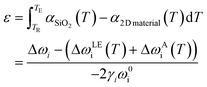 | (15) |
where
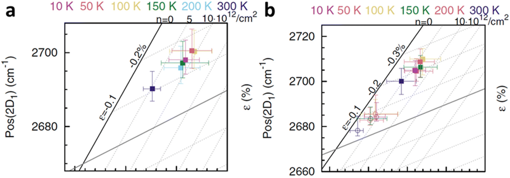
α represents the TEC. The realisation of the temperature-dependent strain and doping model was also attempted by Verhagen
et al.6 to study the cooling effect on monolayer and bilayer isotopically labelled graphene as shown in
Fig. 15a and b respectively. The monolayer graphene is susceptible to the generation of compressive strain when the temperature is reduced from ambient to 100 K; the compression is then saturated at 50 K and even decreases back at 10 K. This compression can be attributed to the TEC mismatch between graphene and SiO
2 substrate.
80 On the other hand, p-doping occurs significantly when the temperature decreases from ambient to 200 K, and the successive cooling does not produce any profound effect. In bilayer, the top layer and bottom layer graphene respond similarly in strain that compression is generated when they are first cooled, which is reduced during further cooling. The doping response between the two layers is different: the p-doping level of the top layer remains almost constant until 10 K and starts to increase after 50 K, while the bottom layer is p-doped when the temperature decreases from ambient to 200 K and the doping level fluctuates beyond that. The temperature induced strain and doping are always stronger in the bottom graphene layer as compared to the top layer, which is due to indirect contact with SiO
2 substrate that the additional graphene layer provides lubricating (weak vdW interface) and charge screening effect.
6
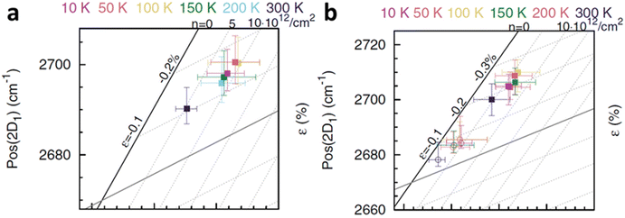 |
| | Fig. 15 Temperature-dependent strain and doping of (a) monolayer graphene and (b) isotopically labelled bilayer graphene. Open circles represent the top layer while filled squares represent the bottom layer. Reprinted with permission from ref. 6 Copyright (2022) from American Physical Society. | |
4. Conclusions
In this review, the fundamentals of strain and doping in 2D materials including graphene and MoS2 are addressed. Under mechanical strain, the change of lattice arrangement leads to a shift in electronic band structure of layered materials, which can be illustrated by the symmetries in hexagonal Brillouin zone for graphene and is related to the transition of direct to indirect band gap for MoS2. Under electrical doping, the relations between applied top gated voltage, surface charge density, and electrical conductivity are extensively demonstrated in different materials. The principles of chemical doping on zero band gap graphene and other semiconductors are also addressed. The combination of strain and doping leads to a shift of Raman modes, which is found to be linearly independent and can be deconvoluted with the help of a correlation plot of Raman peak positions of G and 2D for graphene, and E12g and A1g for MoS2. Several empirical and theoretical methods for the computation of the weightings in such linear transformation, i.e., Grüneisen parameters and doping coefficients, are also presented.
This deconvolution method allows for a non-invasive evaluation of strain and doping of 2D materials on a nanoscopic scale, with higher resolution than conventional techniques such as piezoresistive approaches and field-effect measurements. The simultaneous evaluation of mechanical strain and electrical doping also provides more comprehensive insight than scanning probe techniques such as KPFM, which can only unveil the electrical information.134 The model therefore enables the investigation of a variety of aspects including intrinsic studies, interactions in hybrid vertical heterostructure, corrosion protection, and temperature-dependent studies. An in-depth understanding of the graphene annealing process and its corresponding de-doping results are discussed with the help of correlation plot, where the thermal annealing process can be divided into two steps—a fast doping stage attributed to adsorption of oxygen molecules beneath graphene, and a slow doping stage due to electron transfer in redox reaction. The intrinsic studies of pristine CVD and ME 2D materials show a transition of tensile strain to compressive strain in graphene wrinkles depending on the wrinkles configuration (standing collapsed orientation or transitional-folded). A reduction in p-doping is also observed for graphene wrinkles due to less coupling with the substrate. Recent studies also suggest the generation of patterned compressive strain by depositing 2D materials on a textured surface such that the local strain can be engineered for flexible devices.
The strain and doping studies of hybrid vertical heterostructure become possible thanks to the deconvolution method. The extensive investigation on the interplay between graphene and hBN layers shows that hBN provides protection and charge screening to graphene. Similar inspections are carried out for Gr/MoS2 and Gr/AgNW heterostructure where different contributions to mechanical strain and charge transfer are unveiled by the correlation plot. The release of compressive strain in graphene by the oxide formation and the change in carrier concentration in graphene by the acid corrosion in Gr/Cu demonstrates the feasibility of graphene serving as a chemical sensor. Temperature dependent strain and doping deconvolution allow the computation of TEC and the analysis of the modulation on materials behaviour in low temperature environment. The above applications demonstrate that the strain and doping deconvolution provide an intriguing insight into the emerging field of straintronics where graphene and other 2D materials can be engineered into innovative flexible electronics. The Raman based diagnostic readout is also capable of onsite detection of chemical oxidation and corrosion. Moreover, most biological species which are not Raman active can be exclusively detected from the perspective of 2D materials in terms of strain and doping which is relatively fast and non-invasive than other conventional techniques. Future directions include constructing the strain and doping model to other 2D materials whose Raman active modes are sensitive to mechanical deformation and electronic doping. The determination of the Grüneisen parameters and doping rate of the material could enable the linear transformation of the deconvolution. However, the requirement of possessing two Raman modes which are both independently sensitive to strain and doping limits the employment of this model to many other 2D materials. To date, only graphene and MoS2 are reported to fulfil this prerequisite.22,35,69 It is also possible to apply the model to a variety of research fields such as medical screening, gas sensing and flexible optoelectronics by observing the modulation of strain or doping by foreign molecules, corrosion or oxidation.
Author contributions
FL and MT wrote the manuscript with assistance from RSS, SPO, AAG, IJ and ABD.
Conflicts of interest
There are no conflicts to declare.
Acknowledgements
MT and ABD would like to acknowledge Sussex Strategic Development fund. MT and FL would like to thank Prof. Konstantinos Papagelis (University of Thessaloniki, Greece) and Dr John Parthenios (FORTH/ICE-HT, Greece) for useful discussions.
References
- A. Molina-Sanchez and L. Wirtz, Phys. Rev. B: Condens. Matter Mater. Phys., 2011, 84, 155413 CrossRef.
- J. H. Chen, C. Jang, S. Adam, M. S. Fuhrer, E. D. Williams and M. Ishigami, Nat. Phys., 2008, 4, 377–381 Search PubMed.
- H. Pinto and A. Markevich, Beilstein J. Nanotechnol., 2014, 5, 1842–1848 Search PubMed.
- O. Frank, J. Vejpravova, V. Holy, L. Kavan and M. Kalbac, Carbon, 2014, 68, 440–451 CrossRef CAS.
- F. Lee, M. Tripathi, P. Lynch and A. B. Dalton, Appl. Sci., 2020, 10, 5157 CrossRef CAS.
- T. G. A. Verhagen, K. Drogowska, M. Kalbac and J. Vejpravova, Phys. Rev. B: Condens. Matter Mater. Phys., 2015, 92, 125437 CrossRef.
- L. Yu, Y.-H. Lee, X. Ling, E. J. G. Santos, Y. C. Shin, Y. Lin, M. Dubey, E. Kaxiras, J. Kong and H. Wang, Nano Lett., 2014, 14, 3055–3063 CrossRef CAS PubMed.
- T. M. G. Mohiuddin, A. Lombardo, R. R. Nair, A. Bonetti, G. Savini, R. Jalil, N. Bonini, D. M. Basko, C. Galiotis and N. Marzari, Phys. Rev. B: Condens. Matter Mater. Phys., 2009, 79, 205433 CrossRef.
- G. Ahn, H. R. Kim, T. Y. Ko, K. Choi, K. Watanabe, T. Taniguchi, B. H. Hong and S. Ryu, ACS Nano, 2013, 7, 1533–1541 CrossRef CAS PubMed.
- A. Das, S. Pisana, B. Chakraborty, S. Piscanec, S. K. Saha, U. V. Waghmare, K. S. Novoselov, H. R. Krishnamurthy, A. K. Geim and A. C. Ferrari, Nat. Nanotechnol., 2008, 3, 210–215 CrossRef CAS PubMed.
- A. Mescola, G. Paolicelli, S. P. Ogilvie, R. Guarino, J. G. McHugh, A. Rota, E. Iacob, E. Gnecco, S. Valeri and N. M. Pugno, Small, 2021, 17, 2104487 CrossRef CAS PubMed.
- E. Y. Andrei, G. Li and X. Du, Rep. Prog. Phys., 2012, 75, 056501 CrossRef PubMed.
- B. G. Shin, G. H. Han, S. J. Yun, H. M. Oh, J. J. Bae, Y. J. Song, C. Y. Park and Y. H. Lee, Adv. Mater., 2016, 28, 9378–9384 CrossRef CAS PubMed.
- M. Tripathi, F. Lee, A. Michail, D. Anestopoulos, J. G. McHugh, S. P. Ogilvie, M. J. Large, A. A. Graf, P. J. Lynch and J. Parthenios, ACS Nano, 2021, 15, 2520–2531 CrossRef CAS PubMed.
- C. Lee, H. Yan, L. E. Brus, T. F. Heinz, J. Hone and S. Ryu, ACS Nano, 2010, 4, 2695–2700 CrossRef CAS PubMed.
- K. S. Novoselov, A. K. Geim, S. V. Morozov, D. Jiang, M. I. Katsnelson, I. Grigorieva, S. Dubonos and A. Firsov, Nature, 2005, 438, 197–200 CrossRef CAS PubMed.
- X. Zhang, Z. Shao, X. Zhang, Y. He and J. Jie, Adv. Mater., 2016, 28, 10409–10442 CrossRef CAS PubMed.
- S. D. Costa, J. E. Weis, O. Frank, M. Fridrichová and M. Kalbac, RSC Adv., 2016, 6, 72859–72864 RSC.
- M. S. Bronsgeest, N. Bendiab, S. Mathur, A. Kimouche, H. T. Johnson, J. Coraux and P. Pochet, Nano Lett., 2015, 15, 5098–5104 CrossRef CAS PubMed.
- G. Cocco, E. Cadelano and L. Colombo, Phys. Rev. B: Condens. Matter Mater. Phys., 2010, 81, 241412 CrossRef.
- J. Yan, Y. Zhang, P. Kim and A. Pinczuk, Phys. Rev. Lett., 2007, 98, 166802 CrossRef PubMed.
- A. Michail, D. Anestopoulos, N. Delikoukos, J. Parthenios, S. Grammatikopoulos, S. A. Tsirkas, N. N. Lathiotakis, O. Frank, K. Filintoglou and K. Papagelis, 2D Mater., 2020, 8, 015023 CrossRef.
- D. Rhodes, S. H. Chae, R. Ribeiro-Palau and J. Hone, Nat. Mater., 2019, 18, 541–549 CrossRef CAS PubMed.
- M. Drögeler, F. Volmer, M. Wolter, B. Terrés, K. Watanabe, T. Taniguchi, G. Güntherodt, C. Stampfer and B. Beschoten, Nano Lett., 2014, 14, 6050–6055 CrossRef PubMed.
- J. Chaste, A. Missaoui, S. Huang, H. Henck, Z. Ben Aziza, L. Ferlazzo, C. Naylor, A. Balan, A. T. C. Johnson Jr. and R. Braive, ACS Nano, 2018, 12, 3235–3242 CrossRef CAS PubMed.
-
A. K. Geim and K. S. Novoselov, in Nanoscience and technology: a collection of reviews from nature journals, World Scientific, 2010, pp. 11–19 Search PubMed.
- F. Schedin, A. K. Geim, S. V. Morozov, E. W. Hill, P. Blake, M. I. Katsnelson and K. S. Novoselov, Nat. Mater., 2007, 6, 652–655 CrossRef CAS PubMed.
- B. Chakraborty, A. Bera, D. V. S. Muthu, S. Bhowmick, U. V. Waghmare and A. K. Sood, Phys. Rev. B: Condens. Matter Mater. Phys., 2012, 85, 161403 CrossRef.
- A. Armano, G. Buscarino, M. Cannas, F. M. Gelardi, F. Giannazzo, E. Schilirò and S. Agnello, Carbon, 2018, 127, 270–279 CrossRef CAS.
- J. Vejpravova, B. Pacakova, J. Endres, A. Mantlikova, T. Verhagen, V. Vales, O. Frank and M. Kalbac, Sci. Rep., 2015, 5, 1–9 Search PubMed.
- T. Vincent, V. Panchal, T. Booth, S. R. Power, A.-P. Jauho, V. Antonov and O. Kazakova, 2D Mater., 2018, 6, 015022 CrossRef.
- Z. Peng, X. Chen, Y. Fan, D. J. Srolovitz and D. Lei, Light: Sci. Appl., 2020, 9, 1–25 CrossRef PubMed.
- W. Bao, X. Cai, D. Kim, K. Sridhara and M. S. Fuhrer, Appl. Phys. Lett., 2013, 102, 042104 CrossRef.
- U. Lee, Y. Han, S. Lee, J. S. Kim, Y. H. Lee, U. J. Kim and H. Son, ACS Nano, 2019, 14, 919–926 CrossRef PubMed.
- R. Rao, A. E. Islam, S. Singh, R. Berry, R. K. Kawakami, B. Maruyama and J. Katoch, Phys. Rev. B, 2019, 99, 195401 CrossRef CAS.
- G. Paolicelli, M. Tripathi, V. Corradini, A. Candini and S. Valeri, Nanotechnology, 2015, 26, 055703 CrossRef CAS PubMed.
- G. Chilkoor, N. Shrestha, A. Kutana, M. Tripathi, F. C. Robles Hernández, B. I. Yakobson, M. Meyyappan, A. B. Dalton, P. M. Ajayan and M. M. Rahman, ACS Nano, 2020, 15, 447–454 CrossRef PubMed.
- D.-H. Cho, L. Wang, J.-S. Kim, G.-H. Lee, E. S. Kim, S. Lee, S. Y. Lee, J. Hone and C. Lee, Nanoscale, 2013, 5, 3063–3069 RSC.
- N. Levy, S. A. Burke, K. L. Meaker, M. Panlasigui, A. Zettl, F. Guinea, A. H. C. Neto and M. F. Crommie, Science, 2010, 329, 544–547 CrossRef CAS PubMed.
- V. M. Pereira and A. H. C. Neto, Phys. Rev. Lett., 2009, 103, 046801 CrossRef PubMed.
- Q. H. Wang, Z. Jin, K. K. Kim, A. J. Hilmer, G. L. C. Paulus, C.-J. Shih, M.-H. Ham, J. D. Sanchez-Yamagishi, K. Watanabe and T. Taniguchi, Nat. Chem., 2012, 4, 724–732 CrossRef CAS PubMed.
- C. Lee, X. Wei, J. W. Kysar and J. Hone, science, 2008, 321, 385–388 CrossRef CAS PubMed.
- J. Xue, J. Sanchez-Yamagishi, D. Bulmash, P. Jacquod, A. Deshpande, K. Watanabe, T. Taniguchi, P. Jarillo-Herrero and B. J. LeRoy, Nat. Mater., 2011, 10, 282–285 CrossRef CAS PubMed.
- B. Amorim, A. Cortijo, F. De Juan, A. G. Grushin, F. Guinea, A. Gutiérrez-Rubio, H. Ochoa, V. Parente, R. Roldán and P. San-Jose, Phys. Rep., 2016, 617, 1–54 CrossRef CAS.
- L. Dou, A. B. Wong, Y. Yu, M. Lai, N. Kornienko, S. W. Eaton, A. Fu, C. G. Bischak, J. Ma and T. Ding, Science, 2015, 349, 1518–1521 CrossRef CAS PubMed.
- A. Molle, J. Goldberger, M. Houssa, Y. Xu, S.-C. Zhang and D. Akinwande, Nat. Mater., 2017, 16, 163–169 CrossRef CAS PubMed.
- N. Ferralis, J. Mater. Sci., 2010, 45, 5135–5149 CrossRef CAS.
- H. J. Conley, B. Wang, J. I. Ziegler, R. F. Haglund Jr., S. T. Pantelides and K. I. Bolotin, Nano Lett., 2013, 13, 3626–3630 CrossRef CAS PubMed.
- H. Li, A. W. Contryman, X. Qian, S. M. Ardakani, Y. Gong, X. Wang, J. M. Weisse, C. H. Lee, J. Zhao and P. M. Ajayan, Nat. Commun., 2015, 6, 1–7 CAS.
- K. S. Novoselov, A. K. Geim, S. V. Morozov, D.-e. Jiang, Y. Zhang, S. V. Dubonos, I. V. Grigorieva and A. A. Firsov, Science, 2004, 306, 666–669 CrossRef CAS PubMed.
- B. Radisavljevic, A. Radenovic, J. Brivio, V. Giacometti and A. Kis, Nat. Nanotechnol., 2011, 6, 147–150 CrossRef CAS PubMed.
- F. Schwierz, Nat. Nanotechnol., 2010, 5, 487–496 CrossRef CAS PubMed.
- L. Gomez, I. Aberg and J. L. Hoyt, IEEE Electron Device Lett., 2007, 28, 285–287 CAS.
- A. C. Ferrari, J. C. Meyer, V. Scardaci, C. Casiraghi, M. Lazzeri, F. Mauri, S. Piscanec, D. Jiang, K. S. Novoselov and S. Roth, Phys. Rev. Lett., 2006, 97, 187401 CrossRef CAS PubMed.
- S. Pisana, M. Lazzeri, C. Casiraghi, K. S. Novoselov, A. K. Geim, A. C. Ferrari and F. Mauri, Nat. Mater., 2007, 6, 198–201 CrossRef CAS PubMed.
- X. Lu, M. I. B. Utama, X. Wang, W. Xu, W. Zhao, M. H. S. Owen and Q. Xiong, Small, 2017, 13, 1701039 CrossRef PubMed.
- E. Lorchat, G. Froehlicher and S. Berciaud, ACS Nano, 2016, 10, 2752–2760 CrossRef CAS PubMed.
- B. R. Carvalho, L. M. Malard, J. M. Alves, C. Fantini and M. A. Pimenta, Phys. Rev. Lett., 2015, 114, 136403 CrossRef PubMed.
- C. K. Maiti, Solid-State Electron., 2004, 8, 1255 CrossRef.
- S. Piscanec, M. Lazzeri, F. Mauri, A. C. Ferrari and J. Robertson, Phys. Rev. Lett., 2004, 93, 185503 CrossRef CAS PubMed.
- J. Maultzsch, S. Reich, C. Thomsen, H. Requardt and P. Ordejón, Phys. Rev. Lett., 2004, 92, 075501 CrossRef CAS PubMed.
- Y.-R. Lee, J.-X. Huang, J.-C. Lin and J.-R. Lee, J. Phys. Chem. C, 2017, 121, 27427–27436 CrossRef CAS.
- Y. C. Cheng, Z. Y. Zhu, G. S. Huang and U. Schwingenschlögl, Phys. Rev. B: Condens. Matter Mater. Phys., 2011, 83, 115449 CrossRef.
- S. Piscanec, M. Lazzeri, J. Robertson, A. C. Ferrari and F. Mauri, Phys. Rev. B: Condens. Matter Mater. Phys., 2007, 75, 035427 CrossRef.
- S. Ryu, L. Liu, S. Berciaud, Y.-J. Yu, H. Liu, P. Kim, G. W. Flynn and L. E. Brus, Nano Lett., 2010, 10, 4944–4951 CrossRef CAS PubMed.
- C. Casiraghi, S. Pisana, K. S. Novoselov, A. K. Geim and A. C. Ferrari, Appl. Phys. Lett., 2007, 91, 233108 CrossRef.
- J. E. Lee, G. Ahn, J. Shim, Y. S. Lee and S. Ryu, Nat. Commun., 2012, 3, 1–8 Search PubMed.
- M. Tripathi, A. King, G. Fratta, M. Meloni, M. Large, J. P. Salvage, N. M. Pugno and A. B. Dalton, ACS Omega, 2018, 3, 17000–17009 CrossRef CAS PubMed.
- A. Michail, N. Delikoukos, J. Parthenios, C. Galiotis and K. Papagelis, Appl. Phys. Lett., 2016, 108, 173102 CrossRef.
- Y. Wang, C. Cong, C. Qiu and T. Yu, Small, 2013, 9, 2857–2861 CrossRef CAS PubMed.
- J. E. Proctor, E. Gregoryanz, K. S. Novoselov, M. Lotya, J. N. Coleman and M. P. Halsall, Phys. Rev. B: Condens. Matter Mater. Phys., 2009, 80, 073408 CrossRef.
- F. Ding, H. Ji, Y. Chen, A. Herklotz, K. Dörr, Y. Mei, A. Rastelli and O. G. Schmidt, Nano Lett., 2010, 10, 3453–3458 CrossRef CAS PubMed.
- J. Zabel, R. R. Nair, A. Ott, T. Georgiou, A. K. Geim, K. S. Novoselov and C. Casiraghi, Nano Lett., 2012, 12, 617–621 CrossRef CAS PubMed.
- C. Metzger, S. Rémi, M. Liu, S. V. Kusminskiy, A. H. Castro Neto, A. K. Swan and B. B. Goldberg, Nano Lett., 2010, 10, 6–10 CrossRef CAS PubMed.
- T. Jiang, Z. Wang, X. Ruan and Y. Zhu, 2D Mater., 2018, 6, 015026 CrossRef.
- C. Rice, R. J. Young, R. Zan, U. Bangert, D. Wolverson, T. Georgiou, R. Jalil and K. S. Novoselov, Phys. Rev. B: Condens. Matter Mater. Phys., 2013, 87, 081307 CrossRef.
- M. Tripathi, R. Garriga, F. Lee, S. P. Ogilvie, A. A. Graf, M. Large, P. Lynch, K. Papagelis, J. N. Parthenios and V. L. Cebolla, 2D Mater., 2022, 9, 045033 CrossRef.
- Z. Lin, W. Liu, S. Tian, K. Zhu, Y. Huang and Y. Yang, Sci. Rep., 2021, 11, 1–9 CrossRef PubMed.
- T. Verhagen, V. Vales, O. Frank, M. Kalbac and J. Vejpravova, Carbon, 2017, 119, 483–491 CrossRef CAS.
- D. Yoon, Y.-W. Son and H. Cheong, Nano Lett., 2011, 11, 3227–3231 CrossRef CAS PubMed.
- W. Chen, X. Gui, L. Yang, H. Zhu and Z. Tang, Nanoscale Horiz., 2019, 4, 291–320 RSC.
- J. H. Lee, A. Avsar, J. Jung, J. Y. Tan, K. Watanabe, T. Taniguchi, S. Natarajan, G. Eda, S. Adam and A. H. Castro Neto, Nano Lett., 2015, 15, 319–325 CrossRef CAS PubMed.
- S. Schumacher, T. O. Wehling, P. Lazic, S. Runte, D. F. Förster, C. Busse, M. Petrovic, M. Kralj, S. Blügel and N. Atodiresei, Nano Lett., 2013, 13, 5013–5019 CrossRef CAS PubMed.
- P. L. Levesque, S. S. Sabri, C. M. Aguirre, J. Guillemette, M. Siaj, P. Desjardins, T. Szkopek and R. Martel, Nano Lett., 2011, 11, 132–137 CrossRef CAS PubMed.
- H. Xu, Y. Chen, J. Zhang and H. Zhang, Small, 2012, 8, 2833–2840 CrossRef CAS PubMed.
- F. R. Bagsican, A. Winchester, S. Ghosh, X. Zhang, L. Ma, M. Wang, H. Murakami, S. Talapatra, R. Vajtai and P. M. Ajayan, Sci. Rep., 2017, 7, 1–10 CrossRef CAS PubMed.
- A. Piazza, F. Giannazzo, G. Buscarino, G. Fisichella, A. La Magna, F. Roccaforte, M. Cannas, F. M. Gelardi and S. Agnello, Phys. Status Solidi A, 2016, 213, 2341–2344 CrossRef CAS.
- J. Zhang, J. Xiao, X. Meng, C. Monroe, Y. Huang and J.-M. Zuo, Phys. Rev. Lett., 2010, 104, 166805 CrossRef PubMed.
- K. Zhang and M. Arroyo, J. Appl. Phys., 2013, 113, 193501 CrossRef.
- W. Zhu, T. Low, V. Perebeinos, A. A. Bol, Y. Zhu, H. Yan, J. Tersoff and P. Avouris, Nano Lett., 2012, 12, 3431–3436 CrossRef CAS PubMed.
- T. Verhagen, B. Pacakova, M. Bousa, U. Hübner, M. Kalbac, J. Vejpravova and O. Frank, Sci. Rep., 2019, 9, 1–7 CrossRef CAS PubMed.
- F. Long, P. Yasaei, R. Sanoj, W. Yao, P. Král, A. Salehi-Khojin and R. Shahbazian-Yassar, ACS Appl. Mater. Interfaces, 2016, 8, 18360–18366 CrossRef CAS PubMed.
- A. A. Graf, S. P. Ogilvie, H. J. Wood, C. J. Brown, M. Tripathi, A. A. K. King, A. B. Dalton and M. J. Large, Chem. Mater., 2020, 32, 6213–6221 CrossRef CAS.
-
V. P. Gupta, Molecular and Laser Spectroscopy, 2022, DOI:10.1016/C2020-0-03784-9.
- M. Hosseini, M. Elahi, M. Pourfath and D. Esseni, IEEE Trans. Electron Devices, 2015, 62, 3192–3198 CAS.
- Z. Liu, M. Amani, S. Najmaei, Q. Xu, X. Zou, W. Zhou, T. Yu, C. Qiu, A. G. Birdwell and F. J. Crowne, Nat. Commun., 2014, 5, 1–9 Search PubMed.
- S. H. Choi, Y. J. Kim, W. Yang and K. K. Kim, J. Korean Phys. Soc., 2019, 74, 1032–1038 CrossRef CAS.
- Y. Zhang, M. Heiranian, B. Janicek, Z. Budrikis, S. Zapperi, P. Y. Huang, H. T. Johnson, N. R. Aluru, J. W. Lyding and N. Mason, Nano Lett., 2018, 18, 2098–2104 CrossRef CAS PubMed.
- I. Meric, M. Y. Han, A. F. Young, B. Ozyilmaz, P. Kim and K. L. Shepard, Nat. Nanotechnol., 2008, 3, 654–659 CrossRef CAS PubMed.
- L. Britnell, R. V. Gorbachev, R. Jalil, B. D. Belle, F. Schedin, A. Mishchenko, T. Georgiou, M. I. Katsnelson, L. Eaves and S. V. Morozov, Science, 2012, 335, 947–950 CrossRef CAS PubMed.
- K. S. Novoselov, O. A. Mishchenko, O. A. Carvalho and A. H. Castro Neto, Science, 2016, 353, aac9439 CrossRef CAS PubMed.
- L. T. Zhuravlev, Colloids Surf., A, 2000, 173, 1–38 CrossRef CAS.
- L. Liu, S. Ryu, M. R. Tomasik, E. Stolyarova, N. Jung, M. S. Hybertsen, M. L. Steigerwald, L. E. Brus and G. W. Flynn, Nano Lett., 2008, 8, 1965–1970 CrossRef CAS PubMed.
- W. G. Cullen, M. Yamamoto, K. M. Burson, J.-H. Chen, C. Jang, L. Li, M. S. Fuhrer and E. D. Williams, Phys. Rev. Lett., 2010, 105, 215504 CrossRef CAS PubMed.
- N. M. R. Peres, Rev. Mod. Phys., 2010, 82, 2673 CrossRef CAS.
- S. D. Sarma, S. Adam, E. H. Hwang and E. Rossi, Rev. Mod. Phys., 2011, 83, 407 CrossRef.
- R. V. Gorbachev, I. Riaz, R. R. Nair, R. Jalil, L. Britnell, B. D. Belle, E. W. Hill, K. S. Novoselov, K. Watanabe and T. Taniguchi, Small, 2011, 7, 465–468 CrossRef CAS PubMed.
- W. Bao, F. Miao, Z. Chen, H. Zhang, W. Jang, C. Dames and C. N. Lau, Nat. Nanotechnol., 2009, 4, 562–566 CrossRef CAS PubMed.
- M. Yankowitz, K. Watanabe, T. Taniguchi, P. San-Jose and B. J. LeRoy, Nat. Commun., 2016, 7, 1–8 Search PubMed.
- F. Zheng, K.-i. Sasaki, R. Saito, W. Duan and B.-L. Gu, J. Phys. Soc. Jpn., 2009, 78, 074713 CrossRef.
- W. Zhang, C.-P. Chuu, J.-K. Huang, C.-H. Chen, M.-L. Tsai, Y.-H. Chang, C.-T. Liang, Y.-Z. Chen, Y.-L. Chueh and J.-H. He, Sci. Rep., 2014, 4, 1–8 Search PubMed.
- W. J. Yu, Y. Liu, H. Zhou, A. Yin, Z. Li, Y. Huang and X. Duan, Nat. Nanotechnol., 2013, 8, 952–958 CrossRef CAS PubMed.
- T. Georgiou, R. Jalil, B. D. Belle, L. Britnell, R. V. Gorbachev, S. V. Morozov, Y.-J. Kim, A. Gholinia, S. J. Haigh and O. Makarovsky, Nat. Nanotechnol., 2013, 8, 100–103 CrossRef CAS PubMed.
- W. H. Chae, J. D. Cain, E. D. Hanson, A. A. Murthy and V. P. Dravid, Appl. Phys. Lett., 2017, 111, 143106 CrossRef.
- A. Tiberj, M. Rubio-Roy, M. Paillet, J. R. Huntzinger, P. Landois, M. Mikolasek, S. Contreras, J. L. Sauvajol, E. Dujardin and A. A. Zahab, Sci. Rep., 2013, 3, 1–6 Search PubMed.
- T. Gong, J. Zhang, Y. Zhu, X. Wang, X. Zhang and J. Zhang, Carbon, 2016, 102, 245–254 CrossRef CAS.
- Z. Yan, J. Lin, Z. Peng, Z. Sun, Y. Zhu, L. Li, C. Xiang, E. L. Samuel, C. Kittrell and J. M. Tour, ACS Nano, 2012, 6, 9110–9117 CrossRef CAS PubMed.
- R. He, L. Zhao, N. Petrone, K. S. Kim, M. Roth, J. Hone, P. Kim, A. Pasupathy and A. Pinczuk, Nano Lett., 2012, 12, 2408–2413 CrossRef CAS PubMed.
- S. J. Chae, F. Güneş, K. K. Kim, E. S. Kim, G. H. Han, S. M. Kim, H. J. Shin, S. M. Yoon, J. Y. Choi and M. H. Park, Adv. Mater., 2009, 21, 2328–2333 CrossRef CAS.
- R. Van Gastel, A. J. Martínez-Galera, J. Coraux, H. Hattab, D. Wall, F.-J. M. Zu Heringdorf, M. Horn-von Hoegen, J. M. Gómez-Rodríguez, B. Poelsema and C. Busse, New J. Phys., 2009, 11, 113056 CrossRef.
- H. Mei, R. Huang, J. Y. Chung, C. M. Stafford and H.-H. Yu, Appl. Phys. Lett., 2007, 90, 151902 CrossRef.
- H.-H. Yu and J. W. Hutchinson, Int. J. Fract., 2002, 113, 39–55 CrossRef.
- B. Pacakova, J. Vejpravova, A. Repko, A. Mantlikova and M. Kalbac, Carbon, 2015, 95, 573–579 CrossRef CAS.
- R. Wu, L. Gan, X. Ou, Q. Zhang and Z. Luo, Carbon, 2016, 98, 138–143 CrossRef CAS.
- D. Luo, X. You, B.-W. Li, X. Chen, H. J. Park, M. Jung, T. Y. Ko, K. Wong, M. Yousaf and X. Chen, Chem. Mater., 2017, 29, 4546–4556 CrossRef CAS.
- J. Kwak, Y. Jo, S.-D. Park, N. Y. Kim, S.-Y. Kim, H.-J. Shin, Z. Lee, S. Y. Kim and S.-Y. Kwon, Nat. Commun., 2017, 8, 1–12 CrossRef CAS PubMed.
- M. Nolan and S. D. Elliott, Phys. Chem. Chem. Phys., 2006, 8, 5350–5358 RSC.
- Y. Yang, Z. Lin, R. Li, Y. Li, W. Liu, S. Tian, K. Zhu and L. Long, Microstructures, 2021, 1, 2021002 Search PubMed.
- J. J. Bae, H. Y. Jeong, G. H. Han, J. Kim, H. Kim, M. S. Kim, B. H. Moon, S. C. Lim and Y. H. Lee, Nanoscale, 2017, 9, 2541–2547 RSC.
- S. Sahoo, A. P. S. Gaur, M. Ahmadi, M. J. F. Guinel and R. S. Katiyar, J. Phys. Chem. C, 2013, 117, 9042–9047 CrossRef CAS.
- N. Bonini, M. Lazzeri, N. Marzari and F. Mauri, Phys. Rev. Lett., 2007, 99, 176802 CrossRef PubMed.
- I. Calizo, A. A. Balandin, W. Bao, F. Miao and C. N. Lau, Nano Lett., 2007, 7, 2645–2649 CrossRef CAS PubMed.
- A. T. Apostolov, I. N. Apostolova and J. M. Wesselinowa, J. Phys.: Condens. Matter, 2012, 24, 235401 CrossRef CAS PubMed.
- S. Pak, J. Lee, A. R. Jang, S. Kim, K. H. Park, J. I. Sohn and S. Cha, Adv. Funct. Mater., 2020, 30, 2002023 CrossRef CAS.
Footnote |
| † Authors contributed equally. |
|
| This journal is © The Royal Society of Chemistry 2023 |
Click here to see how this site uses Cookies. View our privacy policy here. 
 Open Access Article
 This Open Access Article is licensed under a
  *a,
Manoj
Tripathi†
*a,
Manoj
Tripathi†
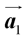 and
and 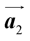 where
where 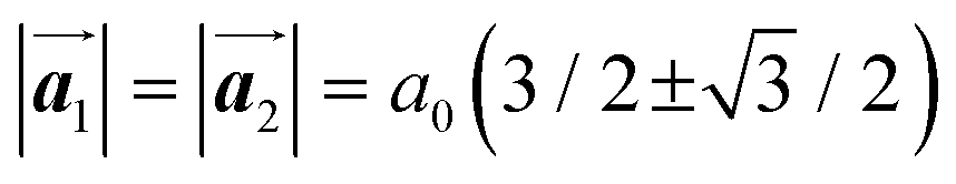 and a0 is the carbon–carbon separation of 0.14 nm. The straining of graphene affects its lattice vector and its associated electronic band structure. The three-dimensional point group of a graphene crystal is D6h.44 It has been observed that under hydrostatic strain for deformation up to 15%, no such significant change in D6h (6/mm) symmetry appears in the hexagonal lattice apart from pseudo gaps at G and M points, but Dirac point (DP) is clamped to the K point (Fig. 1b). Nevertheless, non-hydrostatic strain such as uniaxial strain lowers the symmetry of the graphene lattice associated to sixfold and threefold rotational symmetries. There is a transition from hexagonal D6h (6/mm) to rhombic D2h (mmm); also, the triangular shape Brillouin Zone (BZ) is converted into a polygon, as shown in Fig. 1c and d. The pseudo gap between K and K′ increases under the effect of strain for both armchair and zig-zag configuration. Accordingly, the DP is also shifted from high-symmetry points within the BZ. Under the effect of shear strain, graphene lattice symmetry is transformed to monoclinic, a further lower symmetry class associated to symmetry group 2/m. It has been observed that shear strain causes band gap opening in the graphene far enough from the failure strain.14 Thus, modulation in the electronic band is possible without compromising the mechanical stability of graphene through shear straining (Fig. 1e).20 These effects are investigated through phonon dispersion of graphene through acoustic phonon modes (A) and optical phonon modes (O) of graphene unit cell. The combination of these phonon modes is useful to evaluate the out-of-plane and in-plane vibration of the carbon atoms through Raman scattering.47
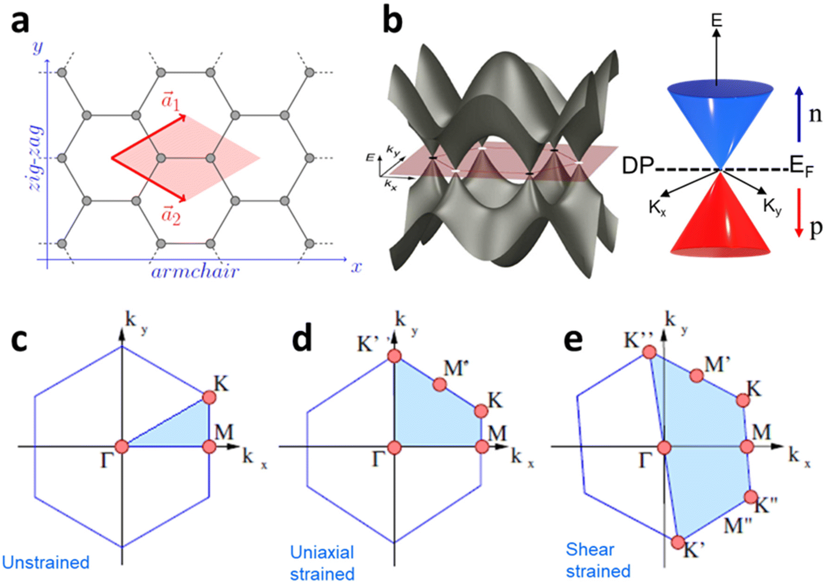
 and
and  . The shaded area represents the unit cell. The inequal crystallographic direction armchair along x-axis and zigzag along y-axis. (b) The high-symmetry (K) points of the hexagonal Brillouin zone (G, M, K) with a representation of characteristic linear bands intersecting at the Dirac point (DP) overlapped with Fermi energy level (EF) for unstrained and doped graphene. The shift of EF either to n or p leads to n-type and p-type doping respectively. Reprinted with permission from ref. 12 Copyright (2022) from IOP Publishing. (c–e) Illustration of BZ of graphene under strain. Reprinted with permission from ref. 20 Copyright (2022) from American Physical Society.
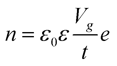


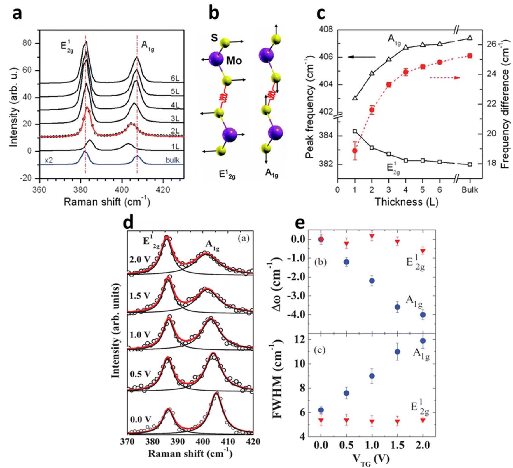

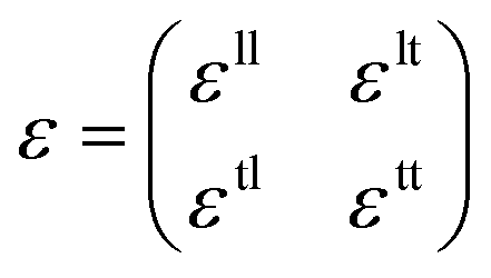
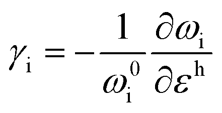
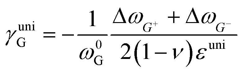
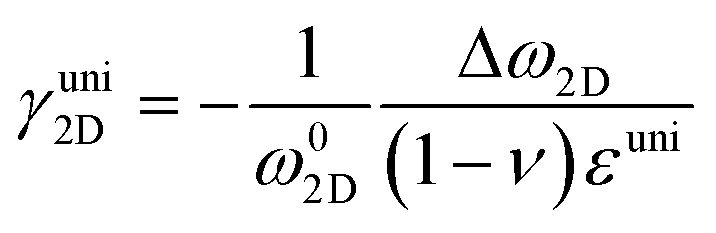
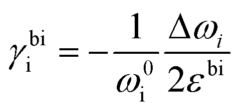
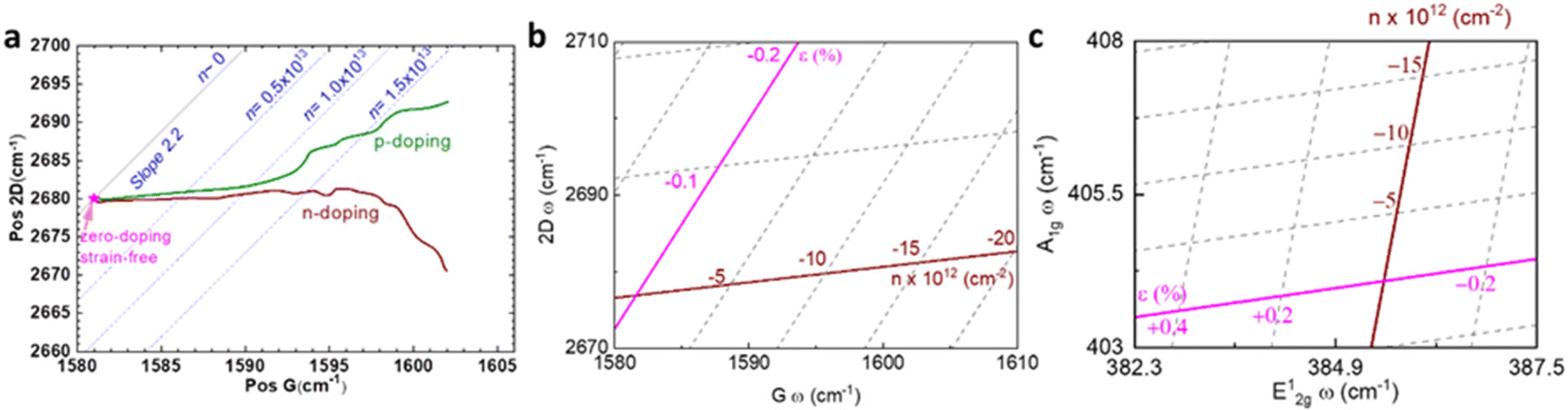
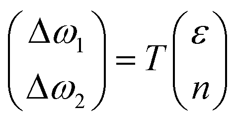
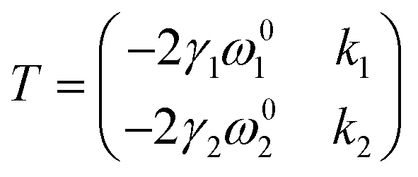
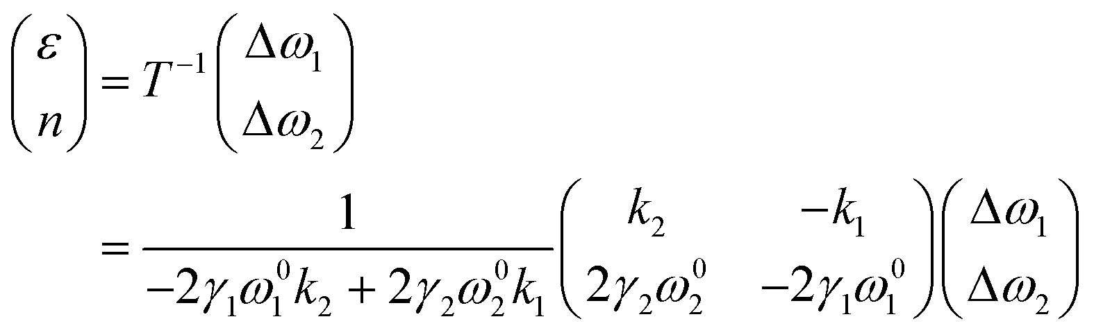
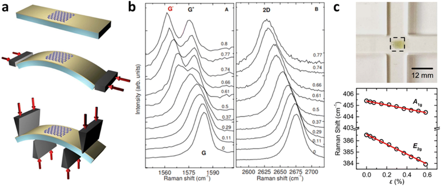
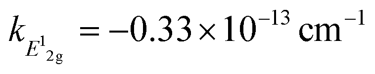 and kA1g = −2.22 × 10⁻¹³ cm−1.28