
 Open Access Article
 This Open Access Article is licensed under a
 Creative Commons Attribution 3.0 Unported Licence
Area-selective Ru ALD by amorphous carbon modification using H plasma: from atomistic modeling to full wafer process integration†
Ivan
Zyulkov‡
 *ab,
Ekaterina
Voronina
cd,
Mikhail
Krishtab
ab,
Dmitry
Voloshin
d,
B. T.
Chan
b,
Yuri
Mankelevich
d,
Tatyana
Rakhimova
d,
Silvia
Armini
b and
Stefan
De Gendt
ab
*ab,
Ekaterina
Voronina
cd,
Mikhail
Krishtab
ab,
Dmitry
Voloshin
d,
B. T.
Chan
b,
Yuri
Mankelevich
d,
Tatyana
Rakhimova
d,
Silvia
Armini
b and
Stefan
De Gendt
ab
aKU Leuven, Department of Chemistry, Faculty of Science, B-3001 Leuven, Belgium. E-mail: ivan.zyulkov@gmail.com
bImec, Kapeldreef 75, B-3001 Leuven, Belgium
cLomonosov Moscow State University, Faculty of Physics, Leninskie Gory, GSP-1, Moscow 119991, Russian Federation
dLomonosov Moscow State University, Skobeltsyn Institute of Nuclear Physics, Leninskie Gory, GSP-1, Moscow 119991, Russian Federation
First published on 22nd October 2020
Abstract
Selective deposition of various materials on pre-defined areas on the substrate is of crucial importance nowadays for microelectronic technology. Carbon-based layers, such as self-assembled monolayers and polymerized fluorocarbon etch residues are often used as passivation layers in order to inhibit the deposition of the required material. In our previous paper, we reported on selective ALD of Ru enabled by H2 plasma passivation of amorphous carbon (a-C) as the non-growth surface and simultaneous activation of a SiCN growth surface. In the present work, we demonstrate a-C modification by H radicals in the absence of H ions in a downstream plasma chamber. The H radical treatment significantly improves the ALD selectivity with respect to the standard H2 plasma treatment by reducing the number of unwanted hydroxyl groups on the a-C surface and providing strong chemical modification of the a-C via surface hydrogenation. In addition, the H radical treatment results in the zero-damage of the a-C film and, therefore, it does not change the pattern profile or the aspect ratio. The experimental data and the investigation of the interaction mechanism between H2 plasma and the a-C surface were supported by molecular dynamic modeling, where effects of the a-C modification by H ions and H radicals were decoupled. The chemical modification of the a-C surface by H radicals results in 10 nm Ru being deposited on Si-based dielectric substrates, while no Ru can be detected by high-resolution RBS on a-C. The H radical surface treatment was also tested on patterned structures with 45 nm half-pitch a-C lines on the SiCN surface.
Introduction
Despite the fact that current lithographic methods are able to print structures with critical dimensions (CD) below 10 nm, alignment of multilevel pattern structures is a significant issue nowadays for further development of microelectronic technology.1 An elegant solution to the problem was found by using area-selective deposition (ASD) processes, allowing deposition of metals and dielectrics on pre-defined areas on the substrate.1 As a result, the development of ASD processes is crucially important for further scaling of integrated circuits (IC).There is a variety of relevant materials being explored, however the main ALD processes can be grouped in four categories: dielectric deposition on a dielectric substrate (DoD), dielectric on metal (DoM), metal on metal (MoM) and metal on dielectric (MoD) depositions. All these processes are under investigation for various applications and provide a “toolkit” to enable future IC scaling despite lithography limitations. The focus of this work is set on MoD deposition processes. A relevant example of an application of selective MoD deposition is a tone-inversion process, as shown in the schematics in Fig. 1.
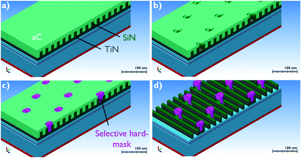 | ||
| Fig. 1 (a–d) Proposed tone-inversion flow. Adopted by Briggs et al.2 | ||
As can be seen in Fig. 1a–c, a selective metal hard-mask growth is required on TiN and SiN surfaces, while metal growth should be inhibited on the a-C surface. When ASD of the metal is achieved on the underlying TiN film, the holes etched in the a-C can be selectively filled with the metal. In a next step, the metal is used as a block cut hard-mask for a-C and SiN etch to form pillars, as shown in Fig. 1d. As already reported in the literature, ALD of Ru demonstrates no nucleation delay and good adhesion on TiO2, TiN and Si-based dielectrics.3,4 In addition, Ru has high etch resistance in H2/N2 and Cl2/Ar/N2-based plasmas used to pattern C-based dielectric materials and TiN/TiO2 films, respectively.5–7 As a result, Ru can be used as a hard-mask for tone-inversion patterning applications in combination with various combinations of materials.2 In addition, according to our previous work, Ru can also be used as a selective catalyst for ASD of Cu by electroless deposition (ELD).4
There are different ways to achieve an inhibition of material growth on a dielectric surface. Typically, surface sensitive deposition techniques are used, such as ELD8 and ALD.4,9,10 In some of the cases, a deposition technique possesses intrinsic selectivity to the material combination used in the stack. A relevant example of this is bottom-up via pre-fill by ELD.8,11 However, most of the applications require the deposition of inhibitors on the non-growth areas to block the deposition. These inhibitors are often carbon-based, such as self-assembled monolayers (SAMs),12–15 fluorocarbon polymers16 and various a-C films.4 The non-growth surface of tone-inversion processing flow shown in Fig. 1 is also made of a-C material, often used as a sacrificial pattern transfer layer. It should be noted, that while SAMs already possess the surface functionality required for the ALD growth inhibition, a-C dielectrics should be modified by surface treatments in order to achieve the desired passivation of the a-C surface.4,17
In our previous work, it has been demonstrated that capacity-coupled H2 plasma (CCP) changes a-C surface functionalities enhancing a-C surface hydrophobicity which leads to a delay in the nucleation of Ru ALD when the EBECHRu ALD precursor is used.4 Furthermore, in the work of E. Stevens et al., H-based treatment of a-C was used to inhibit the ALD of TiN, TiO2, and HfO2 on the a-C surface.17 While the experimental demonstration of the favorable a-C modification in H2 plasma has been consolidated, a detailed study on the mechanisms of a-C modification in H2 plasma and the role of H ions and H radicals in the surface modification process is lacking. In the present work, we optimized the H2 plasma treatment in order to minimize a-C etch, change of critical dimension (CD) and aspect ratio loss, while maximizing the surface functionalization and hydrophobic properties of a-C, required for ALD Ru inhibition using the EBECHRu precursor. In order to support our findings and explore the mechanisms of a-C modification in H2 plasma, density-functional theory modelling of H-radicals and H-ion interaction with the a-C surface was performed.
In order to investigate the a-C etch rate under different H2 plasma conditions, spectroscopic ellipsometry (SE) measurements were employed. X-ray photoelectron spectroscopy (XPS) and static water contact angle (WCA) measurements were used in order to analyze the chemical modification of a-C in H2 plasma. In order to assess the selectivity of Ru ALD, Ru nucleation was quantitatively investigated by Rutherford backscattering spectrometry (RBS). Patterned profiles of a-C lines were characterized by scanning electron microscopy (SEM) before and after ALD Ru deposition.
Materials and methods
Materials
This study was performed on SiCN (Fig. S1, ESI†) and a-C layers4,17 deposited on Si wafers. Both a-C and SiCN films were deposited by plasma-enhanced chemical vapor deposition (PECVD) at 400 °C and 350 °C, respectively, on top of a 1 nm native oxide grown on the p-type Si substrate. All Ru films were deposited by ALD in a cross-flow hot-wall reactor from (ethylbenzyl) (1-ethyl-1,4-cyclohexadienyl) Ru(0) (EBECHRu, C16H22Ru, Hansol Chemical, South Korea), and O2 as a co-reactant. This process has a distinct advantage since it shows a linear nucleation on SiO2 with close to zero inhibition time18 and a smooth grown film (rms roughness is close to 1.0 nm for a 20 nm thick film). The temperature in the reactor was maintained at 275 °C.Plasma steps
The H2 plasma treatments were carried out on 300 mm wafers in a commercial dual-frequency capacitively coupled plasma (CCP) reactor. Remote He/H2 plasma treatments were performed on 300 mm wafers in a downstream remote plasma reactor. The plasma conditions employed in this study are summarized in Table 1.| Plasma | Pressure, mTorr | Power, W | Remarks |
|---|---|---|---|
| a In a downstream plasma setup, only H radicals can reach the sample surface. High energy H ions are confined within the remote plasma source by an ion grid. | |||
| H2 | 5 | 400 | ICP plasma etch to form patterned lines in a-C17 |
| He/H2 | 3000 | 2000 | Downstream plasma sourcea, modification of a-C by H radicals, He/H2 ratio is 30/1 |
Modeling
The simulation of the capacitively coupled plasma (CCP) discharge in pure H2 was carried out on the basis of a previously developed Particle-in-cell with Monte Carlo Collision (PIC MCC) model19 in order to estimate fluxes and energies of H+, H2+ and H3+ ions and H radicals. The configuration of the chamber used in this modelling corresponds to a 300 mm CCP plasma reactor with a discharge radius of 20 cm and an interelectrode gap of 4 cm. The simulation was performed for the following discharge parameters: excitation frequency of 60 MHz, pressure of 50 mTorr and discharge input power of 300 W. In addition, calculations with a discharge input power of 100 W were performed to analyze the impact of the plasma power on the a-C surface modification and to account for possible power loss in the impedance matchbox.Simulations of the interaction between the a-C surface and hydrogen plasma were carried out using the molecular dynamic method. The simulations take into account the a-C damage accumulation and the formation of defects in the a-C film during plasma exposure.20–23 In order to describe H-C interaction, the AIREBO bond-order force field was used. AIREBO considers the formation and breakage of chemical bonds and it was developed especially for hydrocarbon materials.24 An initial a-C model with a volume of 2.5 × 2.5 × 15 nm3 was used to simulate 120 eV H+ ion bombardment, while models of the same lateral size but smaller depths were applied for 120 eV H3+ ions and thermal (0.03 eV) H radicals in order to decrease the calculation time. Two atomic layers at the bottom of the model were fixed, and periodic boundary conditions were applied in XY directions. At the initial moment of the time cycle, a H ion or a H radical was created with a given kinetic energy with random (X, Y) coordinates above the a-C surface. Ions were directed along the Z axis towards the model (normal incidence), and radicals move at different angles (0–45° to the surface normal). To keep the overall temperature of the system at 300 K, the Berendsen thermostat algorithm was periodically used in accordance with the approach proposed by M. Timonova et al. In this approach the first 1.0 ps of the simulation was performed in the microcanonical ensemble with no temperature control to guarantee a proper development of heat cascade, and then the thermostat was switched on in order to cool the model down to 300 K.25 In the first part of this cycle, the time step was chosen equal to 0.02 fs, and in the second part with the thermostat applied, it was increased up to 0.1 fs, so the total duration of one cycle was 5 ps.
The simulations were performed using LAMMPS software on the equipment of the shared research facilities of High-Performance Computing (HPC) centrum at Lomonosov Moscow State University (MSU).26 Visualization of models and analysis of structural changes were carried out in the software package OVITO.
Characterization
The thickness of the dielectric layers was analyzed by spectroscopic ellipsometry (SE) measurements on a Spectra FX CD from KLA-Tencor 300 mm tool. A one-layer model based on Cauchy approximation was used to fit the spectra collected in the wavelength range of 400–800 nm. The chemical composition of the dielectric films was measured via XPS. The measurements were carried out in a Theta 300 system from Thermo Instruments, using a monochromatized Al Kα X-ray source (1486.6 eV) and a spot size of 400 micrometers in an angle integrated mode. Standard sensitivity factors were used to convert peak areas to atomic concentrations. Long-term repeatability of composition analysis has been shown to be close to 1%. The surface concentration of ruthenium was measured by RBS. The RBS data analysis was performed using Imec in-house developed software. He+ beam was used (1.523 MeV), with a scattering angle of 170°, a sample tilt angle of 11°, a beam current on sample of 22 nA, a detector offset of 49.2 keV, a gain of 2.8 keV and a FWHM of 1.7 × 10⁻² MeV. For the WCA measurements, a DataPhysics Contact Angle System OCA model OCAH 230L together with SCA20 software, a CCD camera from Teli and a Hamilton 500 μl syringe were used. Measurements were performed using 1 μl droplets and fitting was done with the ellipse model. A SU8000TM Hitachi SEM tool was used to visualize the top surface morphology and cross-sectional area of the patterned a-C lines. The manual cleaving method was used for SEM sample preparation.Experimental results
As reported in earlier work, CCP H2 plasma results in a-C etch with an etch rate of 50 nm min−1 at 300 W plasma power.4 In order to prevent a-C etch, CD change and aspect ratio loss of patterned a-C structures, remote He/H2 plasma from a downstream plasma source was used. In this plasma setup, H radicals can reach the sample surface, while energetic H ions are confined within the remote plasma source. Blanket 300 mm a-C layers were exposed to remote He/H2 plasma for 1 minute at different temperatures from 65 °C to 250 °C. Lower and higher temperatures cannot be reached in the experimental setup used in this work. Thickness of a-C was measured by SE in order to calculate the etch rate, as shown in Fig. 2a.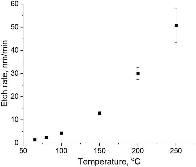 | ||
| Fig. 2 H radicals based etch rate of a-C as a function of substrate process temperature. | ||
As can be seen in Fig. 2, the etch rate of a-C is close to zero at 65 °C, which suggests that a-C cannot be etched by H-radicals at a temperature of 65 °C and below. However, the etch rate increases exponentially with the temperature of the downstream plasma treatment. The calculated activation energy of the a-C etch is 28.4 ± 0.1 kJ mol−1. For comparison reasons, the a-C etch rate in CCP H2 plasma can be around 40 nm min−1.4
In order to investigate the a-C surface modification, WCA and XPS were used, as shown in Fig. 3. According to Fig. 3a, the C1s shoulder peak at a binding energy of 286.5 eV and above is attributed to C–O bonds. The maximum intensity of the C–O peak is observed for the pristine a-C film, which can be attributed to the oxidation of the PECVD a-C after the deposition. The peak intensity decreases with decreasing plasma treatment temperature, which suggests the removal of hydroxyl surface groups from the a-C surface during H radical treatment. As can be seen in Fig. 3b, O1s peak intensity also decreases with decreasing treatment temperature.
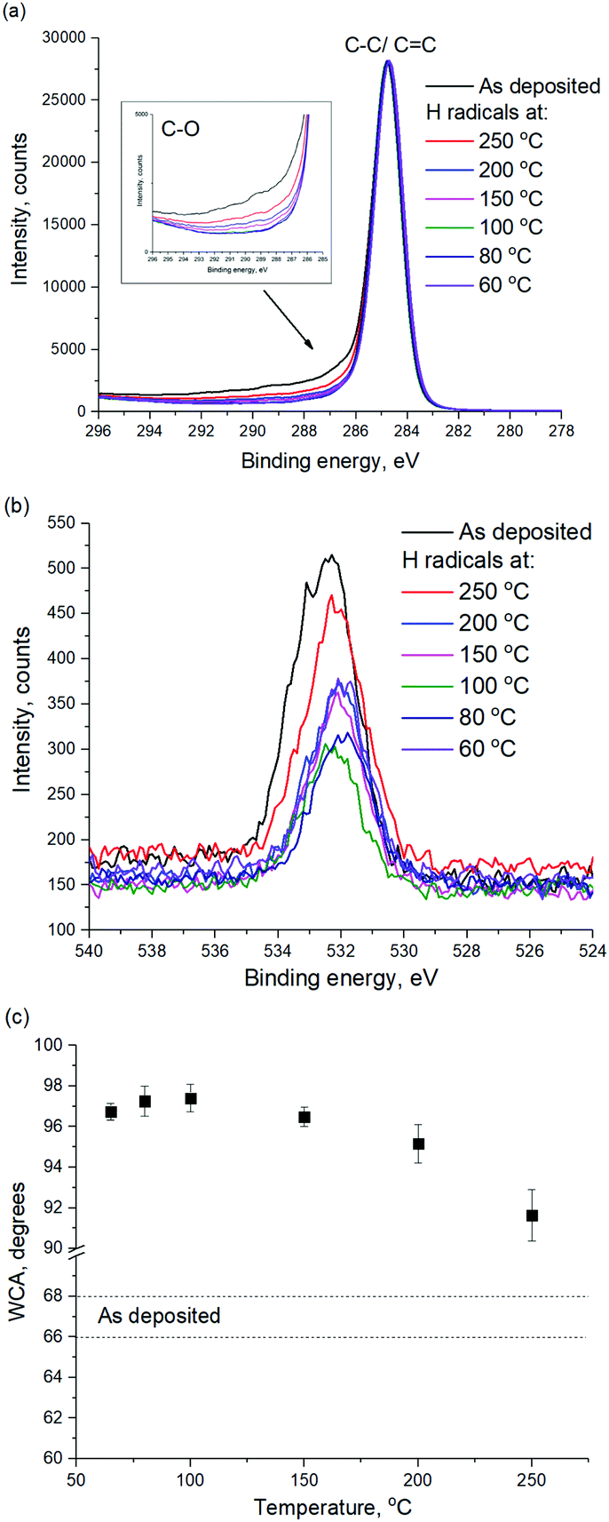 | ||
| Fig. 3 (a) C1s and (b) O1s XPS spectra of a-C before and after remote H plasma treatment at various temperatures, (c) WCA of a-C before and after remote H plasma treatment at various temperatures. | ||
It is suggested that there are two simultaneous processes ongoing during the a-C modification by H radicals: (i) C–C bond breaking with subsequent dangling bond oxidation during ambient exposure resulting in a-C hydroxylation, (ii) hydrogenation of the a-C surface and formation of new hydrophobic methyl groups. The decrease of the H radical treatment temperature leads to less C–C bonds breaking as evident from Fig. 2, therefore, less hydroxyl groups are formed and the effect of the surface hydrogenation is more pronounced. In order to support this conclusion, WCA of a-C surface before and after H radical treatment was measured, as shown in Fig. 3c. As can be seen in Fig. 3c, WCA of a-C increases from 67.5 ± 1.1 to 91.6 ± 1.2 degrees after exposure to H radicals at 250 °C, which suggests the formation of hydrophobic surface groups, such as hydroxyl groups. However, the WCA of a-C increases up to 97.2 ± 0.7 if the plasma treatment is performed at a temperature as low as 100 °C and below. It supports an assumption that a-C etch results in the formation of undesired hydroxyl surface groups on a-C. Therefore, the treatment of a-C with H radicals at the substrate temperature of 80 °C and below provides the highest degree of surface hydrophobization with an a-C etch rate close to zero.
In order to see how the downstream He/H2 plasma surface modification affects the ALD Ru selectivity, a-C samples were exposed to He/H2 plasma treatment at various temperatures and subjected to ALD Ru deposition at 275 °C with the EBECHRu precursor with different number of ALD cycles. Areal density of Ru was quantified by RBS, as shown in Fig. 4. The choice of the ALD deposition temperature is justified by the results of our previous study.4 It has been demonstrated that the nucleation of ALD Ru on a-C using the EBECHRu precursor is strongly inhibited when ALD temperature decreases below 325 °C. At the same time, Ru ALD on the SiCN substrate was not significantly affected by the process temperature in the range of 250–325 °C.
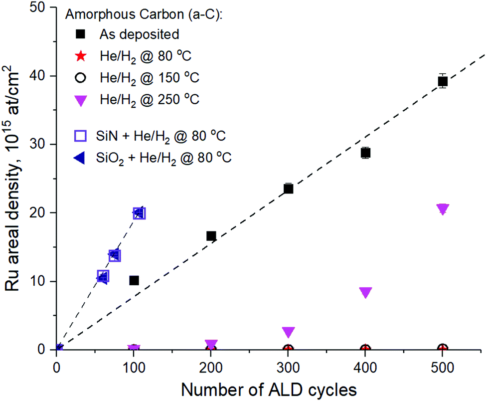 | ||
| Fig. 4 RBS areal density of Ru as a function of ALD cycle number. | ||
As can be seen in Fig. 4, ALD Ru has linear growth per cycle on the pristine a-C surface with the nucleation delay close to zero cycles. However, He/H2 plasma treatment of a-C at 250 °C results in a nucleation delay of 100 cycles and a two-fold decrease of Ru areal density on the a-C surface. Most importantly, a He/H2 plasma temperature decrease down to 150 °C and below results in a Ru nucleation delay of more than 500 cycles on the a-C surface according to high-resolution RBS measurements. The nucleation delay can be explained by low concentration of OH groups on the a-C surface, when the temperature of remote He/H2 plasma is as low as 150 °C and below, as observed by XPS (Fig. 3a). As can be seen in Fig. 4, the nucleation delay of ALD Ru on SiN and SiO2 is close to zero cycles, which can be explained by the affinity of the precursor ligands for OH/NH2 surface groups.4 High concentration of OH/NH2 groups also explains higher Ru growth per cycle (GPC) observed on SiO2 and SiN surfaces compared to the Ru GPS on the a-C surface.3,4 According to the RBS measurement data shown in Fig. 4, the Ru GPC on SiN and SiO2 was calculated as 0.02 nm per cycle assuming a Ru bulk density of 12.36 g cm−3. As a result, around 2 nm of Ru is deposited on SiO2 and SiN in 100 cycles, which is not a fully closed layer.3 Based on GPC, it can be concluded that 10 nm Ru can be deposited on SiO2 and SiN in 500 cycles, while no Ru is present on a-C if remote He/H2 plasma pre-treatment is applied at temperatures below 150 °C. It is expected that other Si-based materials, such as SiCxOy and SiCxNy would also yield a good nucleation of Ru ALD in patterned structures after the plasma etching step is applied. According to our previous work,4 SiCxNy can be damaged by H2-based plasma due to the scission of C–Si and C–N bonds, resulting in C and N loss from the layer and in the formation of the SiO2 surface after the wafer is exposed to an ambient atmosphere.
In order to investigate the ALD Ru selectivity enabled by H radicals on patterned structures, a-C lines with 45 nm half-pitch landed on a SiCN layer were formed via an ICP He/H2 plasma etch process. In this plasma, the a-C layer with SiO2 hard-mask was exposed to H ions and H radicals. Side-view SEM images of a-C lines after the ICP H2 plasma etch process as shown in Fig. 5.
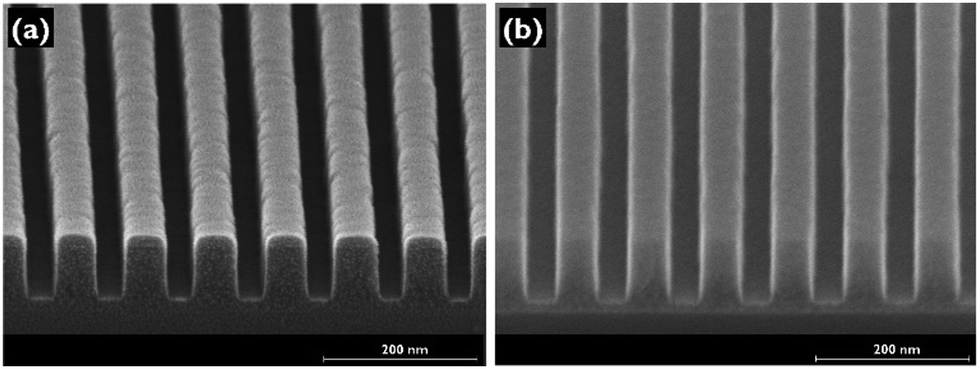 | ||
| Fig. 5 Cross-sectional images of a-C lines after ICP He/H2 plasma (a) before and (b) after SiO2 hard-mask removal as measured via SEM. | ||
After hard-mask removal in diluted HF, the patterned samples were exposed for 10 seconds to remote He/H2 plasma at 80 °C, 150 °C and 250 °C. After the plasma treatment, 100 cycles of ALD Ru were performed on the samples at 275 °C. Cross-sectional images of a-C lines after Ru ALD can be seen in Fig. 6.
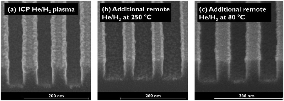 | ||
| Fig. 6 Cross-sectional images of a-C lines after 100 cycles ALD of Ru at 275 °C as measured via SEM. (a) No pre-treatment, remote He/H2 plasma pre-treatment at (b) 250 °C, and (c) 80 °C. | ||
As can be seen in Fig. 6a, when no pre-treatment is used ALD Ru is deposited on both a-C lines and SiCN underlayers. It should be noted that ICP He/H2 plasma used to form a-C lines already provides certain selectivity benefits, when compared to other plasma formulations, such as N2/H2 plasma, as shown in Fig. S2 (ESI†). As can be seen in Fig. 6a, Ru is mainly present on top of the a-C lines and not on the sidewalls, which can be explained by the H ion-induced damage of a-C on the top surface. As was mentioned earlier, plasma-induced damage of a-C carbon can result in a-C surface oxidation leading to Ru nucleation during ALD. As can be seen in Fig. 6b, an additional a-C pre-treatment by H radicals in remote He/H2 plasma at 250 °C results in Ru growth on a-C sidewalls, which can be explained by H radical-induced damage on a-C at 250 °C (Fig. 2a). However, He/H2 plasma pre-treatment at 80 °C (Fig. 6c) considerably decreases the defectivity of ALD Ru. Some Ru defects are present in the corners of the a-C lines, which might be attributed to the SiO2 hard-mask residues. In addition, it can be noted that He/H2 plasma pre-treatment at 80 °C does not result in CD loss, while there is a clear trimming of the a-C lines as observed via CD SEM, when the He/H2 plasma pre-treatment is applied at 250 °C, which is in line with the a-C etch rate data shown in Fig. 2. While there is a certain degree of Ru selectivity improvement observed after He/H2 post-treatment performed at 80 °C, the selectivity of ALD Ru significantly deviates from what is expected based on the blanket results (Fig. 4). Therefore, an additional development is required for the process of integration, e.g. in terms of hard-mask residues cleaning from the corners of the lines.
Modeling results
In order to support the experimental results and to provide an insight on interaction mechanisms of a-C with the H2 plasma, molecular dynamic (MD) modelling was used. First, a model of the plasma discharge was built by particle-in-cell/Monte Carlo collision (PIC MCC) simulation in order to estimate fluxes and energies of H+, H2+ and H3+ ions and H radicals present in the plasma chamber. The parameters obtained from the model, such as plasma density (Ne), voltage amplitude (Vrf), electron temperature (Te) and fluxes of different ions and neutral H atoms can be found in Table 2.| Power, W | N e, cm−3 | V rf | T e, eV | H flux, cm−2 s−1 | H3+ flux, cm−2 s−1 | H2+ flux, cm−2 s−1 | H+ flux, cm−2 s−1 |
|---|---|---|---|---|---|---|---|
| 60 | 1.3 × 10¹⁰ | 180 | 2 | 1.8 × 10¹⁶ | 1.5 × 10¹⁵ | 3.1 × 10¹⁴ | 1.5 × 10¹⁴ |
| 300 | 2.7 × 10¹⁰ | 270 | 1.6 | 2.6 × 10¹⁶ | 2.5 × 10¹⁵ | 5.7 × 10¹⁴ | 3.3 × 10¹⁴ |
According to Table 2, H radicals are the main species in H2 plasma discharge. The flux of H3+ ions is 10 times lower in comparison with the flux of H radicals. The flux of H2+ and H+ ions is 10 times lower in comparison with the flux of H3+ ions. Energy distribution of H ions as well as mean H ion energy is shown in Fig. 7a and b, respectively.
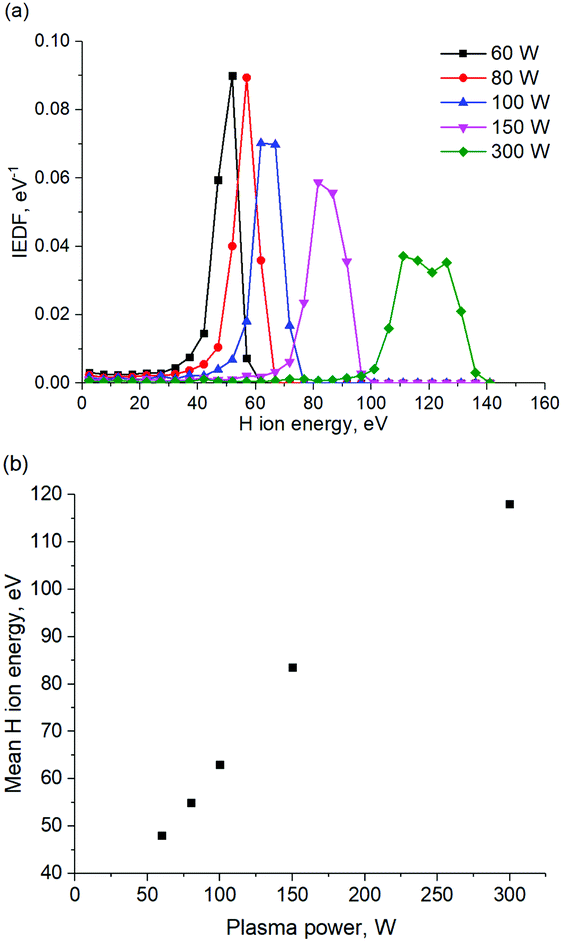 | ||
| Fig. 7 (a) Ion energy distribution function for various plasma power settings obtained in PIC MCC simulation. (b) Mean H ion energy as the function of the plasma power. | ||
According to the energy distribution of H ions, shown in Fig. 7a, the average H ions energy in the plasma discharge is 120 eV at the plasma power of 300 W. It should be noted that the decrease of the plasma power from 300 W to 60 W results in the H ion energy decrease down to 50 eV, as can be seen in Fig. 7a and b. A H ion energy of 120 eV was used for MD simulation, unless stated otherwise.
MD simulations of a-C interaction with the H2 plasma were performed using a bond-order potential. It enables one to consider the formation and breakage of chemical bonds between atoms and to obtain a realistic picture of H ion and radical interaction with the a-C surfaces.
Modelling of a-C interaction with H ions
First, the a-C layer interaction with hydrogen ions was modelled, since the formation of a-C patterned structures requires H ion bombardment.27 Model of a-C consists of carbon with sp, sp2 and sp3 hybridizations with the ratio of 4/65/31, which is in good agreement with the literature data.28 It should be noted that the modelling of a-C interaction with H ions is done under the assumption that a-C consists of C atoms only, while the PECVD a-C layer also contains H atoms. This simplification still allows one to analyse the impact of H ions on a-C bonds (C–C/C![[double bond, length as m-dash]](https://www.rsc.org/images/entities/char_e001.gif) C and C
C and C![[triple bond, length as m-dash]](https://www.rsc.org/images/entities/char_e002.gif) C) and hydrogenation of the a-C layer. Fig. 8 shows side images of the a-C model at different H ion fluences.
C) and hydrogenation of the a-C layer. Fig. 8 shows side images of the a-C model at different H ion fluences.
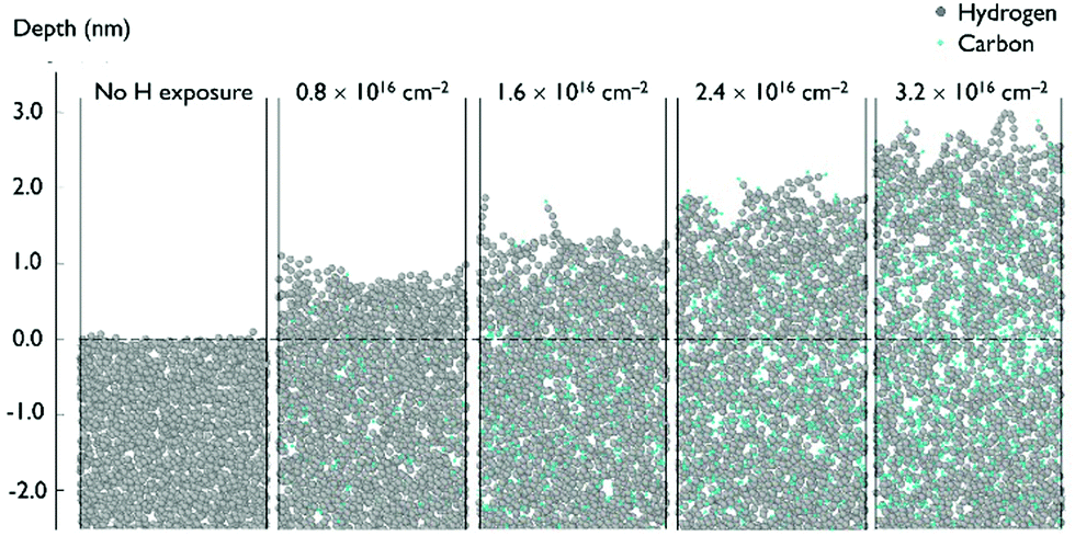 | ||
| Fig. 8 Cross-sectional images of the a-C layer modified by H ions at different ion fluences. | ||
According to the model shown in Fig. 8, penetration of incident H ions into the a-C layer is observed. H ions have a high kinetic energy of 120 eV and a relatively small ion size, which allows them to penetrate deep into the a-C. The maximum penetration depth of ∼6.5 nm was observed for the H ion fluence of 3.2 × 1016 cm−2, which corresponds to ∼20 seconds of H ion exposure. It should be noted that the maximum penetration depth is calculated as the depth of the layer containing less than 1% of all incorporated H atoms. The depth is calculated from the new surface level, which is changing with the H ion fluence. According to Fig. 8, a-C film swelling is observed after film exposure to H ions. The a-C thickness increases by ∼3 nm at a H ion fluence of 3.2 × 1016 cm−2. Film swelling is caused by a-C density decrease due to C–C bond scission as a result of the interaction with the incident H ions. Density of the a-C before and after exposure to H ions is shown in Fig. 9a. The average density of the H-modified a-C layer (defined as the layer with the H concentration exceeding 10%) is ∼1.4 g cm−3, which is substantially lower than the initial a-C density of 2.5 g cm−3.
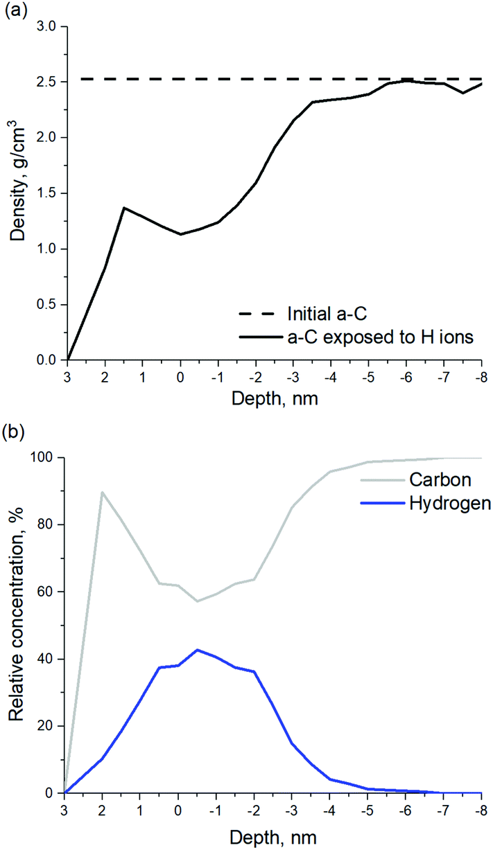 | ||
| Fig. 9 (a) a-C density before and after exposure to H ions. (b) Depth profiles of relative concentrations of C and H atoms at a fluence of 3.2 × 1016 cm−2. | ||
In should be noted, that etching of a-C by H ions was not observed in the model. In order to etch a-C film by H, volatile species, such as methane should be formed.29 As mentioned earlier, H ions with an energy of 120 eV are able to cause C–C bond breaking, however C–H bond formation occurs mainly inside the modified a-C layer, but not on the a-C surface, as can be seen in Fig. 9b. H ion energy decreases by multiple collisions with C atoms and dissipates as the H ion penetrates inside the film, resulting in H implantation. As can be seen in Fig. 9b, a maximum H concentration of ∼40% is achieved at a depth of 3.5 nm from the film surface. Under the H2 plasma experimental conditions, the H ion flux is combined with a flux of H radicals (the flux of H radicals is ten-fold higher as compared to the H ion flux) as can be seen in Table 1. H radicals are able to passivate C dangling bonds, increasing the probability to form methane and, therefore, etch the a-C layer. For this reason, a-C film swelling was not observed experimentally,4 since the modified a-C layer is etched in H2 plasma.
The calculated number of CHx groups formed by a-C exposure to H ions is shown in Fig. 10a as a function of the a-C layer depth. As can be seen in Fig. 10a, 80% of the functional groups in the H-modified near-surface layer of a-C are CH groups. Another 18% are CH2 groups and only ∼2% care CH3 groups.
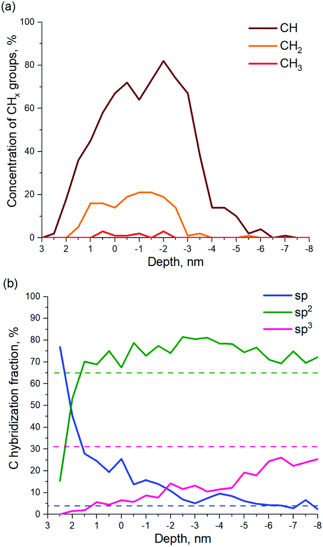 | ||
| Fig. 10 (a) Relative concentration of CHx groups in the H-modified a-C and (b) calculated profiles of carbon hybridization in the H-modified a-C layer. The initial values of sp, sp2 and sp3 hybridization are shown by dashed lines of the corresponding color. | ||
Due to the presence of CHx groups and expected surface roughening, the a-C surface formed by H ions should demonstrate hydrophobic properties.30–32 Increase of the a-C WCA after exposure to CCP H2 plasma is an effect previously observed in the literature.4
Interestingly, despite the C–C bond scission, the formation of new CC and CC is observed in the model, which suggests a restructuration of the a-C film. Fig. 10b shows calculated profiles of carbon hybridization in the H-modified a-C layer. The initial values of sp, sp2 and sp3 hybridization of a-C are shown by dashed lines. As can be seen in Fig. 10b, after the material is exposed to H ions the relative quantity of sp hybridized C atoms increases in the near-surface layers from 4% up to ∼75%. However, inside the modified a-C layer, the sp component decreases with the depth, down to the initial value. The sp3-hybridized fraction of the a-C shows the opposite behavior. The concentration of sp3 fraction is close to 0% on the layer surface, while it rises in the depth of a-C up to its initial value of 31. The sp2-content is 10–15% larger over the whole modified a-C layer. As can be seen in Fig. S3 (ESI†), separate carbon chains mainly consist of sp- and sp2-carbon, which explains the high concentration of sp/sp2 fractions in the near-surface layer of the a-C.
As shown in Fig. 7, H2 plasma power decrease from 300 W to 100 W results in the mean H2 ion energy decrease down to 50 eV. Therefore, an additional calculation of the a-C interaction with H ions with the energy of 50 eV was performed in order to analyze how the plasma power and H2 ion energy affect the a-C modification process. The cross-sectional images of the a-C layer modified by H ions with energies of 50 eV and 120 eV at the ion fluence of 8 × 1015 cm−2 are shown in Fig. S4 (ESI†). It can be concluded that the H ion energy decreases, from 120 eV to 50 eV resulting in the substantial decrease of the H penetration depth from ∼6.5 nm to ∼2.5 nm, as can be concluded from Fig. S5a (ESI†). Therefore, the a-C modification and hydrogenation are better confined within the near-surface layers (Fig. S5a and b, ESI†).
To summarize, it can be concluded that a-C exposure to H ions results in C–C bond scission, leading to a-C layer damage, decrease of a-C density, hydrogenation of a-C and formation of CHx groups. The plasma power decrease results in the substantial decrease of the H ion energy. Lower H ion energy results in lower H ion penetration depth and stronger modification of the near-surface a-C layer. H ions alone do not result in the a-C etch; H radicals are needed in order to form volatile methane species.
Modelling of a-C interaction with H radicals
For the investigation of the a-C modification by H radicals, a model of hydrogenated a-C was used. An initial a-C model containing only C atoms was exposed to 50 eV H ions with the fluence of 8 × 1015 cm−2, which resulted in a hydrogenated a-C model with pronounced modification of the near-surface a-C layer. This allows determination of whether hydrogenated a-C would etch under H radical treatment. The side views of this model are shown in Fig. 11.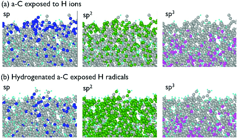 | ||
| Fig. 11 Side view of the a-C model: (a) exposed to 50 eV H ions at the fluence of 8 × 1015 cm−2, and (b) exposed to H ions and H radicals at 300 K and the fluence of 1017 cm−2. | ||
According to Fig. 11, a-C exposure to thermal H radicals influences only near-surface layers of the material. As was observed in the model, H atoms scatter non-reactively at the surface or initiate chemical reactions with C resulting in the appearance of new C–H bonds. According to Fig. 11, thermal H radicals are able to convert triple CC bonds into double CC bonds and double CC bonds into single C–C bonds. This results in the sp2 and sp3 carbon hybridization fraction increase at the expense of sp-hybridized carbon. Fig. 12a presents the relative concentrations of C and H atoms and C atoms with different hybridization.
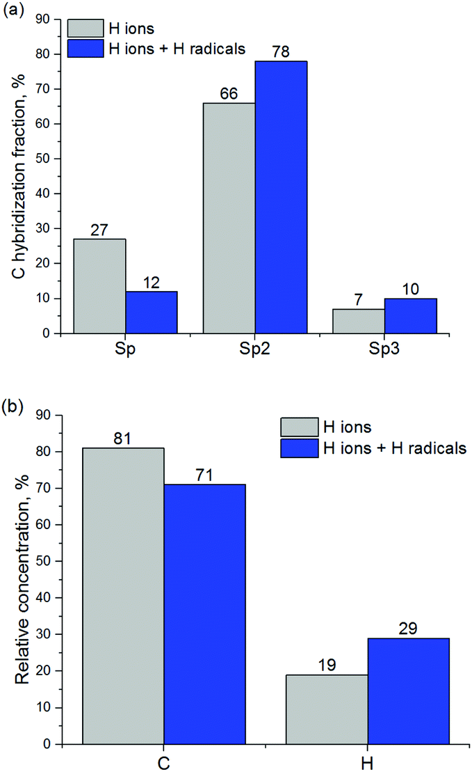 | ||
| Fig. 12 (a) Carbon hybridization fractions and (b) relative concentrations of carbon and hydrogen in a-C before and after exposure to H radicals. | ||
In addition, relative concentrations of C and H atoms were calculated for the a-C layer before and after exposure to H radicals, as shown in Fig. 12b. It can be seen that hydrogen concentration increases after a-C exposure to H radicals, as can also be observed from Fig. 11. H concentration increase should lead to the increase of the concentration of CHx groups, which is important for the improvement of ALD inhibition on the a-C surface.4 It should be noted that all CH3 groups observed during the simulation of a-C interaction with H radicals have been formed from CH2 groups with CC double bonds, by the transformation of the double bond into single carbon bond with subsequent hydrogenation, according to reaction (1).
| CH2 + H(rad) → –CH3 | (1) |
| CH2 + H(rad) → –CH2 | (2) |
As can be concluded from MD modelling, a-C exposure to H-radicals at room temperature does not lead to C–C bond scission and therefore does not result in a-C etch. At the same time, H radicals can break CC double-bonds in favor of C–H bond formation, which results in the formation of CH2 and CH3 groups on the surface. Formation of CHx groups explains the observed ALD Ru inhibition on the a-C surface, due to the unfavorable interaction of EBECHRu precursor molecule ligands with the hydrogen-terminated a-C surface.4,33 It is also shown that the hydrogen ion interaction with the a-C surface leads to C–C bond scission. Combination of H ions and H radicals results in a-C etch. In addition, the formation of carbon dangling bonds by H ions can lead to oxidation of the surface in the atmosphere, resulting in the formation of reactive hydroxyl groups favorable to the ALD Ru process. It can be concluded that H-radicals at near-room temperature are the best a-C treatment for chemical surface modification with no changes in the a-C pattern profile and aspect ratio of the structures.
Conclusions
a-C surface treatment by H radicals using remote He/H2 plasma at 150 °C and below results in a Ru nucleation delay of more than 500 cycles on the a-C surface, while Ru grows on initial a-C without any nucleation delay. The approach was tested on 45 nm half-pitch a-C lines. According to cross-sectional SEM images, a-C treatment by H radicals at 150 °C and below improves the selectivity of ALD Ru.As can be concluded from MD simulations, a-C exposure to H ions results in C–C bonds breaking, a-C density decrease and hydrogenation of the a-C layer. An additional treatment of the a-C by H radicals at room temperature does not lead to C–C bond scission and therefore does not damage the a-C layer. H radicals break CC double-bonds in favor of C–H bond formation, which results in the formation of CH2 and CH3 groups on the a-C surface. Formation of CHx groups explains the observed ALD Ru inhibition on the a-C surface, due to unfavorable interaction of EBECHRu precursor ligands with the hydrogenated a-C surface.
Conflicts of interest
There are no conflicts to declare.Acknowledgements
The authors would like to acknowledge Dr Johan Meersschaut for the RBS and EDX measurements and Dr Thierry Conard for XPS measurements.Notes and references
- R. Clark, K. Tapily, K. H. Yu, T. Hakamata, S. Consiglio, D. O’Meara, C. Wajda, J. Smith and G. Leusink, APL Mater., 2018, 6(5), 058203, DOI:10.1063/1.5026805.
- B. Briggs, I. Zyulkov and K. Devriendt, US Pat., US20180330986, 2018 Search PubMed.
- M. Popovici, B. Groven, K. Marcoen, Q. M. Phung, S. Dutta, J. Swerts, J. Meersschaut, J. A. Van Den Berg, A. Franquet, A. Moussa, K. Vanstreels, P. Lagrain, H. Bender, M. Jurczak, S. Van Elshocht, A. Delabie and C. Adelmann, Chem. Mater., 2017, 29, 4654–4666 CrossRef CAS.
- I. Zyulkov, M. Krishtab, S. De Gendt and S. Armini, ACS Appl. Mater. Interfaces, 2017, 9, 31031–31041 CrossRef CAS.
- C. Zhiying, R. Alok and P. Ventzek, US Pat., US20200051833A1, 2020 Search PubMed.
- D. Wan, S. Paolillo, N. Rassoul, B. K. Kotowska, V. Blanco, C. Adelmann, F. Lazzarino, M. Ercken, G. Murdoch, J. Bömmels, C. J. Wilson and Z. Tokei, 2018 IEEE Int. Interconnect Technol. Conf., IITC 2018, 2018, 10–12.
- S. Paolillo, D. Wan, F. Lazzarino, N. Rassoul, D. Piumi and Z. Tőkei, J. Vac. Sci. Technol., B: Nanotechnol. Microelectron.: Mater., Process., Meas., Phenom., 2018, 36, 03E103 Search PubMed.
- I. Zyulkov, S. Armini, K. Opsomer, C. Detavernier and S. De Gendt, J. Mater. Chem. C, 2019, 15, 4392–4402 RSC.
- M. M. Minjauw, J. Dendooven, B. Capon, M. Schaekers and C. Detavernier, J. Mater. Chem. C, 2014, 3, 132–137 RSC.
- M. M. Minjauw, J. Dendooven, B. Capon, M. Schaekers and C. Detavernier, J. Mater. Chem. C, 2015, 3, 4848–4851 RSC.
- Y. Jiang, P. Nalla, Y. Matsushita, G. Harm, W. Jingyan, A. Kolics, L. Zhao, T. Mountsier, P. Besser and H. J. Wu, 2016 IEEE Int. Interconnect Technol. Conf./Adv. Met. Conf., IITC/AMC 2016, 2016, 111–113.
- C. Prasittichai, K. L. Pickrahn, F. S. Minaye Hashemi, D. S. Bergsman and S. F. Bent, ACS Appl. Mater. Interfaces, 2014, 6, 17831–17836 CrossRef CAS.
- F. Sadat, M. Hashemi, B. R. Birchansky and S. F. Bent, ACS Appl. Mater. Interfaces, 2018, 8(48), 33264–33272 Search PubMed.
- X. Jiang and S. F. Bent, J. Phys. Chem. C, 2009, 113, 17613–17625 CrossRef CAS.
- H. Zhou, J. M. Blackwell, H. B. R. Lee and S. F. Bent, ACS Appl. Mater. Interfaces, 2013, 5, 3691–3696 CrossRef CAS.
- A. Haider, P. Deminskyi, T. M. Khan, H. Eren and N. Biyikli, J. Phys. Chem. C, 2016, 120, 26393–26401 CrossRef CAS.
- E. Stevens, Y. Tomczak, B. T. Chan, E. Altamirano Sanchez, G. N. Parsons and A. Delabie, Chem. Mater., 2018, 30, 3223–3232 CrossRef CAS.
- M. Popovici, A. Redolfi, M. Aoulaiche, J. A. van den Berg, B. Douhard, J. Swerts, P. Bailey, B. Kaczer, B. Groven, J. Meersschaut, T. Conard, A. Moussa, C. Adelmann, A. Delabie, P. Fazan, S. Van Elshocht and M. Jurczak, Microelectron. Eng., 2015, 147, 108–112 CrossRef CAS.
- D. G. Voloshin, Y. A. Mankelevich, O. V. Proshina and T. V. Rakhimova, Plasma Processes Polym., 2017, 14(4–5), 1600119 CrossRef.
- B. N. Jariwala, C. V. Ciobanu, S. Agarwal, B. N. Jariwala, C. V. Ciobanu and S. Agarwal, J. Appl. Phys., 2009, 106.7, 073305 CrossRef.
- V. Martirosyan, O. Joubert and E. Despiau-Pujo, J. Phys. D: Appl. Phys., 2018, 52.5, 055204 Search PubMed.
- A. A. Sycheva, E. N. Voronina, T. V. Rakhimova and A. T. Rakhimov, Appl. Surf. Sci., 2019, 475, 1021–1032 CrossRef CAS.
- A. A. Sycheva, E. N. Voronina, T. V. Rakhimova, A. T. Rakhimov, A. A. Sycheva, E. N. Voronina and T. V. Rakhimova, J. Vac. Sci. Technol., A, 2018, 36(6), 061303 CrossRef.
- S. J. Stuart, A. B. Tutein, J. A. Harrison and S. J. Stuart, J. Chem. Phys., 2000, 112.14, 6472–6486 CrossRef.
- M. Timonova, B. Lee and B. J. Thijsse, Nucl. Instrum. Methods Phys. Res., Sect. B, 2007, 255, 195–201 CrossRef CAS.
- S. A. Z. Vladimir, V. Voevodin, A. S. Antonov, D. A. Nikitenko, P. A. Shvets, S. I. Sobolev, I. Yu. Sidorov, K. S. Stefanov and V. V. Voevodin, Supercomput. Front. Innovations, 2019, 6, 23–35 Search PubMed.
- K. Van Laer, S. Tinck, V. Samara, J. F. de Marneffe and A. Bogaerts, Plasma Sources Sci. Technol., 2013, 22, 025011 CrossRef.
- G. T. Gao, P. T. Mikulski, G. M. Chateauneuf and J. A. Harrison, J. Phys. Chem. B, 2003, 107.40, 11082–11090 CrossRef.
- M. Zarshenas, B. Czerwinski, K. Moshkunov and A. D. Delcorte, J. Phys. Chem. C, 2018, 122(27), 15252–15263 CrossRef CAS.
- Y. Zhou, B. Wang, X. Song, E. Li, G. Li, S. Zhao and H. Yan, Appl. Surf. Sci., 2006, 253.5, 2690–2694 CrossRef.
- M. K. Han, T. Kim, J. H. Cha, D. H. Kim, H. J. Lee and H. J. Lee, Appl. Sci. Convergence Technol., 2017, 26(2), 34–41 CrossRef.
- T. A. R. Hansen, J. W. Weber, P. G. J. Colsters, D. M. H. G. Mestrom, M. C. M. Van De Sanden and R. Engeln, J. Appl. Phys., 2012, 112(1), 013302 CrossRef.
- J. Heo, S.-J. Won, D. Eom, S. Y. Lee, Y. B. Ahn, C. S. Hwang and H. J. Kim, Electrochem. Solid-State Lett., 2008, 11(8), H210 CrossRef CAS.
Footnotes |
| † Electronic supplementary information (ESI) available: Cross-sectional SEM images of a-C lines formed by H2/N2 CCP plasma after 100 cycles of Ru ALD, additional side view images of the upper a-C layer modified by H ions with fluence of 3.2 × 1016 cm−2, comparison of cross-sectional images of the a-C layer modified by 50 eV H ions (100 W) and 120 eV H ions (300 W) as well as depth profiles of relative H concentration and a-C density after exposure of a-C to H ions at 50 eV and 120 eV. See DOI: 10.1039/d0ma00462f |
| ‡ Current address: Umicore, Watertorenstraat 33, 2250 Olen, Belgium. |
| This journal is © The Royal Society of Chemistry 2020 |