
 Open Access Article
 This Open Access Article is licensed under a Creative Commons Attribution-Non Commercial 3.0 Unported Licence
Reconfigurable artificial synapses with an organic antiambipolar transistor for brain-inspired computing†
Ryoma
Hayakawa
 *a,
Yuho
Yamamoto
ab,
Kosuke
Yoshikawa
ab,
Yoichi
Yamada
b and
Yutaka
Wakayama
*a
*a,
Yuho
Yamamoto
ab,
Kosuke
Yoshikawa
ab,
Yoichi
Yamada
b and
Yutaka
Wakayama
*a
aResearch Center for Materials Nanoarchitectonics (MANA), National Institute for Materials Science (NIMS), 1-1 Namiki, Tsukuba 305-0044, Japan. E-mail: WAKAYAMA.Yutaka@nims.go.jp; Tel: +81-29-860-4403
bFaculty of Pure and Applied Sciences, University of Tsukuba 1-1-1 Tennodai, Tsukuba 305-8573, Japan
First published on 12th June 2025
Abstract
Neuromorphic computing, a nonvon Neumann architecture, holds promise for low-power, high-efficiency data processing. Herein, we demonstrated reconfigurable artificial synapses using a floating-gate-type organic antiambipolar transistor (FG-OAAT) to mimic biological synapses. The FG-OAAT exhibited a Λ-shaped transfer curve with negative differential transconductance. A two-dimensional continuous Au film was used as the floating gate to induce a large peak voltage shift in the Λ-shaped transfer curve by controlling hole- and electron-trapping processes in the floating gate. This feature enabled reconfigurable synaptic operations. Long-term potentiation/depression, excitatory/inhibitory, and paired-pulse facilitation/depression functions were electrically reconfigured by tuning the charge conditions in the floating gate. These versatile synaptic operations were induced by a consistent presynaptic signal, with fixed polarity, applied voltage, and pulse width. These behaviors closely resembled those of biological synapses, highlighting the potential for a brain-like computing architecture that surpasses current von Neumann systems.
1. Introduction
The development of high-performance artificial intelligence (AI) is crucial for the upcoming Internet of Everything society owing to the rapid increase in data volumes from versatile information and communication systems including automobile systems, healthcare sensors, and industrial robots.1–6 However, current AI systems based on the von Neumann architecture exhibit high power consumption.7,8 For instance, the power consumption of supercomputer “K” reaches 10 MW.9 This issue arises from the increased access frequency between logic and memory units, known as the von Neumann bottleneck. Therefore, the evolution of energy-efficient AI systems is an essential challenge in the big data era.Neuromorphic computing systems, a type of non von Neumann architecture, offer a solution for energy-efficient AI.10–12 These systems mimic the brain, which operates with ultralow power consumption (20 W) through parallel data processing.13 Neuromorphic devices integrate logic and memory units, with nonvolatile memories such as magnetic random-access memory and ferroelectric memory widely used.14–17 This device configuration enables extremely low-power consumption and high-speed parallel data processing. In addition, the adoption of pulse-based analog operations, such as spiking neural networks, is expected to drive the evolution of highly energy-efficient AI systems.18–20
Organic transistors with nonvolatile memories are widely employed in neuromorphic applications because of their attractive features, including light weight, flexibility, and biocompatibility.21–24 The recognition of complex images and voice patterns has already been demonstrated.25,26 However, conventional organic transistors usually support only synaptic operations for an input signal because they exhibit unipolar carrier transport.21–24 Meanwhile, biological synapses exhibit diverse responses to identical input signals, with synaptic operations reconfigured by neuromodulatory commands.27–30 Accordingly, the development of reconfigurable artificial synapses is a key challenge in the construction of brain-inspired AI systems. To address this, we demonstrate reconfigurable neuromorphic operations based on a floating-gate-type organic antiambipolar transistor (FG-OAAT).
An OAAT is a heterojunction transistor with at least one p–n junction in the transistor channel, which induces negative differential transconductance and produces a Λ-shaped transfer curve.31–37 The drain current increases and then decreases with increasing gate voltage. This unique carrier transport in OAATs has enabled the creation of logic circuits, including ternary and quaternary inverters, ternary logic-in-memory, and reconfigurable two-input logic circuits.38–43
Herein, we applied OAATs to a reconfigurable artificial synapse, using 2,7-dioctyl[1]benzothieno[3,2-b][1]benzothiophene (C8-BTBT) and PhC2H4-benzo[de]isoquinolino[1,8-gh]quinolone diimide (PhC2-BQQDI) films as the p-type and n-type transistor channels, respectively. Notably, a Au film was introduced as the floating gate (FG) to induce a large peak voltage shift in the Λ-shaped transfer curve by controlling the hole- and electron-trapping processes in the FG. This feature enabled unique synaptic operations, with long-term potentiation (LTP)/depression (LTD), excitatory/inhibitory, and paired-pulse facilitation (PPF)/depression (PPD) electrically reconfigured by adjusting the charge conditions of the Au FG. These findings suggest the potential to realize a new computing architecture beyond the current von Neumann computing.
2. Experimental methods
2.1. Formation of FG-OAATs
FG-OAATs with C8-BTBT and PhC2-BQQDI were fabricated on a highly doped p-type Si(100) substrate (< 0.01 Ω cm) with a 200 nm-thick SiO2 layer. First, a Au (30 nm)/Cr (5 nm) electrode was deposited as a back gate (BG) on the SiO2/Si substrate via thermal vacuum deposition. Subsequently, a HfO2 film (35 nm) was prepared as the gate insulating layer using atomic layer deposition (ALD) (SUGA Co. Ltd., SAL 1000), with the substrate temperature set at 175 °C. Here, tetrakis(dimethylamino)hafnium and water were used as the hafnium and oxygen sources, respectively. Afterward, an Au (10 nm)/Cr (5 nm) film was thermally grown on the HfO2 layer as the FG, with a deposition rate of 5 Å s−1 to ensure a smooth surface morphology of the Au thin film. Then, a 10 nm-thick HfO2 tunneling layer was formed via ALD, following the same process as the gate insulating layer. To passivate carrier trap sites on the HfO2 surface, a 10 nm-thick polystyrene (PS) (Sigma-Aldrich, 182427, average molecular weight: 280![[thin space (1/6-em)]](https://www.rsc.org/images/entities/char_2009.gif) 000) layer was spin-coated on the HfO2 surface. Subsequently, C8-BTBT (13 ± 3 nm) and PhC2-BQQDI (8 ± 2 nm) films were grown as p- and n-type organic channels, respectively, via thermal vacuum deposition at a background pressure of 10−7 Pa. Finally, 30 nm-thick Au films were deposited for the source (S) and drain (D) electrodes via thermal vacuum deposition, with typical width and length dimensions of 400 and 200 μm, respectively.
000) layer was spin-coated on the HfO2 surface. Subsequently, C8-BTBT (13 ± 3 nm) and PhC2-BQQDI (8 ± 2 nm) films were grown as p- and n-type organic channels, respectively, via thermal vacuum deposition at a background pressure of 10−7 Pa. Finally, 30 nm-thick Au films were deposited for the source (S) and drain (D) electrodes via thermal vacuum deposition, with typical width and length dimensions of 400 and 200 μm, respectively.
2.2 Transistor measurement
Transistor measurements of the FG-OAATs and neuromorphic operations were performed using a source measure unit (Keysight Technology, B2912B) under atmospheric conditions. All the measurements were conducted with a four-probe system at room temperature.3. Results and discussion
Fig. 1a and b show the device structure and optical microscope image of the FG-OAAT. The transistor features a BG-type structure, with 14 nm-thick C8-BTBT and 8 nm-thick PhC2-BQQDI films as the p- and n-type transistor channels, respectively. The detailed optimization processes of FG-OAATs are described in ESI† (Fig. S1–S5). Fig. 1c and d exhibit a typical drain current (ID)–BG voltage (VBG) curve and the differential transconductance (dID/dVBG) curve for the n-type operation of the FG-OAAT, with the D voltage (VD) fixed at 3.0 V. The transistor exhibited a Λ-shaped transfer curve (Fig. 1c), with no hysteresis appearing in the forward and reverse VBG sweeps (black and red solid lines, respectively, in Fig. 1c), indicating no carrier trapping in the Au FG within the applied voltage range. ID started to increase at VBG (Von) = 0.2 V, reaching 126 nA at VBG (Vpeak) = 1.8 V. Thereafter, ID was completely suppressed at VBG (Voff) = 2.6 V in the forward VBG sweep from 0 to 3.0 V (black solid line in Fig. 1c). A distinct negative differential transconductance was observed between 1.9 and 2.6 V in the forward VBG sweep of up to 3.0 V (Fig. 1d). Additionally, it is noteworthy that the low voltage operation of below 3.0 V was another essential achievement, which is induced by the employment of HfO2 layer as the gate insulating layer. Usually, operation voltages of more than 5.0 V are required for OAATs.31–38 | ||
| Fig. 1 (a) Device structure and (b) optical microscope image of the FG-OAAT, utilizing PhC2-BQQDI and C8-BTBT films as transistor channels, with an Au film serving as the floating gate. (c) ID–VBG and (d) differential transconductance curve of the FG-OAAT measured at VD = 3.0 V. (e) Illustrations of carrier transport in the FG-OAAT across VBG ranges: (a) VBG < Von, (b) Von < VBG < Voff, and (c) Voff < VBG. | ||
In our previous study, the Λ-shaped transfer curves in OAATs were interpreted analogously to the shoot-through current in complementary metal-oxide-semiconductor inverters. Namely, ID of FG-OAATs is the overlapped current of the constituent n-type and p-type transistors described using the following equations:44–47
 | (1) |
 | (2) |
Based on the above argument, the carrier transport process in FG-OAATs can be explained using the illustrations shown in Fig. 1e and f. In VBG < Von region (Fig. 1e), no electron current flows because VBG is below the Vth,n of the PhC2-BQQDI channel. However, holes accumulate in the C8-BTBT channel owing to the applied effective gate voltage (VD–VBG). However, the hole current is suppressed by the potential barrier at the p–n junction, resulting in no ID in the VBG range. In VBG > Von (Fig. 1f), electrons are introduced from the S electrode and flow toward the D electrode. Simultaneously, the accumulated holes in the C8-BTBT channel begin to flow toward the S electrode, generating ID in FG-OAATs. A further increase in VBG (VBG > VoffFig. 1g) hinders ID because the C8-BTBT channel enters the off state.
Next, the Λ-shaped transfer curve in the FG-OAAT can be controlled using the Au FG. Fig. 2a–c illustrate the processes of erasing, electron trapping, and hole trapping. The corresponding ID–VBG curves are depicted in Fig. 2d, where the solid and dotted lines at each state represent the forward and reverse VBG sweeps, respectively. First, the Au FG was grounded to erase the carriers (electrons or holes) in the Au FG, which is defined as the erasing process (Fig. 2a). The resulting ID–VBG curve is exhibited by the black solid and dotted lines in Fig. 2d. Vpeak was estimated at 2.1 V. Then, VBG = 5.0 V was applied for 10 s to trap electrons in the Au FG (Fig. 2b), where the S and D electrodes were grounded. This operation shifted the ID–VBG curve higher VG, as shown by the blue solid and dotted lines in Fig. 2d. Vpeak shifted from 2.1 to 3.1 V. Importantly, no hysteresis was observed in the shifted ID–VBG curve, revealing that the trapped electrons in the Au FG were retained during the VBG sweeps. After the erasing process (Fig. 2a), the opposite BG voltage, VBG = −5.0 V, was applied for 10 s to trap holes in the Au FG (Fig. 2c). As a result, Vpeak shifted to 1.0 V (red solid and dotted line in Fig. 2d). No hysteresis appeared in the ID–VBG curve, similar to the electron-trapped sate. Consequently, the total variation in Vpeak reached 2.1 V by controlling the charge conditions (holes or electrons) in the Au FG. This value is much larger than that observed in our previous study with a zinc-phthalocyanine-core star-shaped polymer (ZnPc-PS4) as the FG.43,48 This improvement in Vpeak shift in this study benefits from using the Au FG.
 | ||
| Fig. 2 (a) Erasing, (b) electron-trapping, and (c) hole-trapping processes of the FG-OAATs. (d) ID–VBG curves for the erased (black line), electron-trapped (blue line), and hole-trapped (red line) states, with solid and dotted lines representing forward and reverse VBG sweeps, respectively. (e) Retention property of the FG-OAAT. (f) Switching behavior of the FG-OAAT. (g) Variation in Vpeak values in electron-trapped and erased states as a function of switching cycles. | ||
Fig. 2e shows the retention property of electron- and hole-trapped states, where the potential of the Au FG was monitored. The trapped electrons and holes were retained for at least 1800 s. The switching behavior between the erased and electron-trapped states of the FG-OAATs is depicted in Fig. 2f and g. After 10 switching cycles, the Vpeak positions after the electron-trapping and releasing processes were almost identical.
Based on these nonvolatile memory properties, we applied the FG-OAAT to a neuromorphic device. For synaptic operations with the FG-OAAT, the BG and D electrodes function as the presynaptic input and postsynaptic output terminals, respectively. ID was monitored as the postsynaptic current (PSC). Fig. 3a shows ID–VBG for the erased (black solid line), electron-trapped (blue solid line), and hole-trapped (red solid line) states. As shown in Fig. 3b–d, a variety of synaptic operations were reconfigured by adjusting the initial charge condition in the Au FG. First, Fig. 3b illustrates the transition from LTP to LTD with the FG-OAAT. Prior to this measurement, the initial ID–VBG curve was set to the electron-trapped state (blue solid line in Fig. 3a) by applying a VBG of 5.0 V for 10 s. PSC (ID,read) was monitored at a VG (VG,read) of 1.8 V and VD (VD,read) of 3.0 V. When negative VBG pulses (VBG = −5.0 V, pluse width (Pwidth) = 100 ms) were applied, ID,read started increasing and was maintained even after the VBG pulses were turned off, indicating the LTP operation. Thereafter, ID,read decreased with identical positive VBG pulses (VBG = 5.0 V, Pwidth = 100 ms), corresponding to the LTD operation. Next, the opposite transition from LTD to LTP was observed as shown in Fig. 3c even with identical sequence of presynaptic pulses (VBG = −5.0 V, Pwidth = 100 ms and VBG = 5.0 V, Pwidth = 100 ms) applied to the transistor. The difference of Fig. 3b and c is the initial charge conditions in the Au FG.
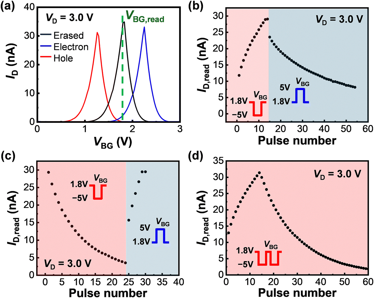 | ||
| Fig. 3 (a) ID–VBG curves at the erased (black line), electron-trapped (blue line), and hole-trapped (red line) states. (b) LTP and LTD operations as a function of presynaptic pulse numbers, with the electron-trapped state defined as the initial state. (c) LTD and LTP as a function of presynaptic pulse numbers, following an erasing operation. I.e., no carriers were trapped in the Au FG. (c) Transition from LTP to LTD induced by continuous presynaptic pulses. | ||
In Fig. 3c, the initial ID–VBG curve was set to the erased state (black solid line in Fig. 3a). As a result, the transition from LTD to LTP was induced by applying the same sequence of VBG pulses with the negative-to-positive polarity change. Finally, Fig. 3d shows that the transition from LTP to LTD can be induced by applying only negative VBG pulses (VBG = −5.0, Pwidth = 100 ms) continuously. (VBG = −5 V, Pwidth = 100 ms) (Fig. 3d). Here, the initial ID–VBG curve was set to the electron-trapped state (blue solid line in Fig. 3a).
The abovementioned results clearly reveal that reconfigurable synaptic operations, transitioning from LTP to LTD and vice versa, can be achieved by controlling the initial charge conditions of the Au FG. Such synaptic plasticity has typically not been demonstrated in conventional transistors, which exhibit unipolar carrier transport.21–26 By contrast, biological synapses are known to display different responses to synaptic plasticity under neuromodulatory control, even when the same polarity, applied voltage, and pulse width are applied.27–30 This suggests that our proposed transistor has the potential to truly mimic biological synapses. Notably, the continuous VBG pulse applications in Fig. 3d enabled a smooth transition from LTP to LTD, while a sharp drop in ID,read was observed in Fig. 3b when the VBG pulse polarity was reversed. The nonlinearity coefficients and asymmetric factors of LTP/LTD behaviors were also improved by the continuous VBG pulse applications (Fig. S6 in ESI†). This improvement offers an additional advantage of using our proposed transistor.
In a similar manner to the LTP/LTD behaviors, excitatory/inhibitory and PPF/PPD operations were electrically reconfigured, as shown in Fig. 4. Fig. 4a shows the ID–VBG curves before (black dotted line) and after (black solid line) the application of a negative VBG pulse (VBG = −5 V for 100 ms), where no carriers were accumulated in the Au FG in the initial state (black dotted line). The corresponding variation in ID,read is depicted in Fig. 4b, where ID,read was monitored at VG,read = 1.2 V and VD,read = 3.0 V. A sharp increase in ID,read from 25 to 40 nA was observed by the application of a negative VBG pulse (VBG = −5 V for 100 ms). Importantly, ID,read was maintained at 30 nA after the VBG pulse was turned off, due to the threshold voltage shift induced by the hole-trapping process in the Au FG. This variation in ID,read corresponds to the excitatory synaptic operation. The synaptic plasticity was changed by the presynaptic input pulse. Moreover, the PPF behavior distinctly appeared with the application of double-negative VBG pulses (VBG = −5 V for 100 ms) (Fig. 4c). The FFP ratio (ID,read,change) was calculated using the following equation:
 | (3) |
 | ||
| Fig. 4 (a) ID–VBG curves before (black dotted line) and after (black solid line) a presynaptic pulse application (VBG = −5 V, Pwidth = 100 ms), with no carriers trapping in the Au FG at the initial state. (b) Excitatory and (c) PPF operations of the FG-OAAT, with VD,read and VG,read set to 3.0 and 1.2 V, respectively; no carriers were accumulated in the Au FG at the initial state in both cases. (d) ID–VBG curves before (red dotted line) and after (red solid line) a presynaptic pulse application (VBG = −5 V, Pwidth = 100 ms), with holes trapped in the Au FG at the initial state. (e) Inhibitory and (f) PPD operations of the FG-OAAT, where holes were accumulated in the Au FG at the initial state. | ||
Strikingly, the opposite synaptic behaviors, namely inhibitory and PPD operations, are shown in Fig. 4d–f, even though the same VBG pulses as in Fig. 4a–c were applied to the transistor. First, the ID–VBG curve was set to the red dotted line in Fig. 4d, where holes were trapped in the Au FG. Then, the application of a negative VBG pulse (VBG = −5 V for 100 ms) shifted the transfer curve from the red dotted line to the solid line (Fig. 4d), leading to a reduction in ID,read, as shown in Fig. 4e. Similarly, PPD was obtained by applying the same double-negative VBG pulses as in Fig. 4c. The PPD ratio was varied from −2.5% at Pinterval = 3.5 s to −28.0% at Pinterval = 0.5 s with a reduction in pulse intervals.
As shown, we realized reconfigurable synaptic operations. Namely, LTP/LTD, inhibitory/excitatory, and PPF/PPD operations were electrically reconfigured by adjusting the charging conditions of the Au FG. Such reconfigurable synaptic operations have not been attained in other neuromorphic devices. Conversely, our transistor enables versatile operations without changing the presynaptic signals, similar to biological synapses. Thus, our proposed transistors have the potential to enable brain-like computing architectures, surpassing the limitations of the current von Neumann model.
4. Conclusions
We achieved reconfigurable artificial synapses with FG-OAAT, using the Au film as the FG. The transistor exhibited a typical Λ-shaped transfer curve. Notably, the Au FG induced a large Vpeak shift in the transfer curve by controlling hole- and electron-trapping processes. This feature was applied to reconfigurable synaptic operations, where excitatory/inhibitory, LTP/LTD, and PPF/PPD behaviors were electrically reconfigured by adjusting the charge conditions of the Au FG. Importantly, these versatile synaptic operations were induced by identical presynaptic input signals, similar to those of the human brains. These findings are expected to pave the way for highly brain-like AI systems, advancing the evolution of computing systems.Author contributions
This manuscript was written through the contributions of all authors.Conflicts of interest
The authors declare no competing financial interest.Data availability
The data that support the findings of this study are available from the corresponding authors upon reasonable request.Acknowledgements
This research was supported by Research Center for Materials Nanoarchitectonics (MANA) of National Institute for Materials Science (NIMS), Tsukuba, Japan, and JSPS Kakenhi grant numbers 19H00866, 22K18268, 23H00269 and 24K01564, the Canon Foundation, Innovative Science & Technology Initiative for Security, and Advanced Research Infrastructure for Materials and Nanotechnology in Japan (ARIM) of the Ministry of Education, Culture, Sports, Science and Technology (MEXT) grant numbers JPMXP1223NM5170 and JPMXP1224NM5158.Notes and references
- S. Feng, H. Sun, X. Yan, H. Zhu, Z. Zou, S. Shen and H. X. Liu, Nature, 2023, 615, 620–627 CrossRef CAS PubMed.
- S. Feng, X. Yan, H. Sun, Y. Feng and H. X. Liu, Nat. Commun., 2021, 12, 748 CrossRef CAS PubMed.
- M. Yip, S. Salcudean, K. Goldberg, K. Althoefer, A. Menciassi, J. D. Opfermann, A. Krieger, K. Swaminathan, C. J. Walsh, H. H. Huang and I.-C. Lee, Science, 2023, 381, 141–146 CrossRef CAS PubMed.
- M. Chen, D. Cui, H. Haick and N. Tang, Adv. Sens. Res., 2024, 3, 2300009 CrossRef.
- C. Xu, S. A. Solomon and W. Gao, Nat. Mach, Intell., 2023, 5, 1344–1355 CrossRef PubMed.
- S. Ambrogio, P. Narayanan, A. Okazaki, A. Fasoli, C. Mackin, K. Hosokawa, A. Nomura, T. Yasuda, A. Chen, A. Friz, M. Ishii, J. Luquin, Y. Kohda, N. Saulnier, K. Brew, S. Choi, I. Ok, T. Philip, V. Chan, C. Silvestre, I. Ahsan, V. Narayanan, H. Tsai and G. W. Burr, Nature, 2023, 620, 768–775 CrossRef CAS PubMed.
- S. Chen, Nature, 2025, 639, 22–24 CrossRef CAS PubMed.
- Q. Chen, J. Wang and J. Lin, Science, 2025, 387, 587 CrossRef CAS PubMed.
- K. Yamamoto, A. Uno, H. Murai1, T. Tsukamoto, F. Shoji, S. Matsui, R. Sekizawa, F. Sueyasu, H. Uchiyama, M. Okamoto, N. Ohgushi, K. Takashina, D. Wakabayashi, Y. Taguchi and M. Yokokawa, Procedia Comput. Sci., 2014, 29, 576–585 CrossRef.
- S. Pazos, K. Zhu, M. A. Villena, O. Alharbi, W. Zheng, Y. Shen, Y. Yuan, Y. Ping and M. Lanza, Nature, 2025, 640, 69–76 CrossRef CAS PubMed.
- G. M. Marega, Y. Zhao, A. Avsar, Z. Wang, M. Tripathi, A. Radenovic and A. Kis, Nature, 2020, 587, 72–77 CrossRef PubMed.
- Y. Wang, H. Tang, Y. Xie, X. Chen, S. Ma, Z. Sun, Q. Sun, L. Chen, H. Zhu, J. Wan, Z. Xu, D. W. Zhang, P. Zhou and W. Bao, Nat. Commun., 2021, 12, 3347 CrossRef CAS PubMed.
- P. A. Merolla, J. V. Arthur, R. Alvarez-Icaza, A. S. Cassidy, J. Sawada, F. Akopyan, B. L. Jackson, N. Imam, C. Guo, Y. Nakamura, B. Brezzo, I. Vo, S. K. Esser, R. Appuswamy, B. Taba, A. Amir, M. D. Flickner, W. P. Risk, R. Manohar and D. S. Modha, Science, 2014, 345, 668–673 CrossRef CAS PubMed.
- L. Danial, E. Pikhay, E. Herbelin, N. Wainstein, V. Gupta, N. Wald, Y. Roizin, R. Daniel and S. Kvatinsky, Nat. Electron., 2019, 2, 596–605 CrossRef CAS.
- S. Jung, H. Lee, S. Myung, H. Kim, S. K. Yoon, S.-W. Kwon, Y. Ju, M. Kim, W. Yi, S. Han, B. Kwon, B. Seo, K. Lee, G.-H. Koh, K. Lee, Y. Song, C. Choi, D. Ham and S. J. Kim, Nature, 2022, 601, 211–216 CrossRef CAS PubMed.
- W.-X. You, B.-K. Huang and P. Su, IEEE Trans. Electron Devices, 2022, 69, 444–446 Search PubMed.
- T. Ohno, T. Hasegawa, T. Tsuruoka, K. Terabe, J. K. Gimzewski and M. Aono, Nat. Mater., 2011, 10, 591–595 CrossRef CAS PubMed.
- A. Stanojevic, S. Woźniak, G. Bellec, G. Cherubini, A. Pantazi and W. Gerstner, Nat. Commun., 2024, 15, 6793 CrossRef CAS PubMed.
- S. S. Radhakrishnan, A. Sebastian, A. Oberoi, S. Das and S. Das, Nat. Commun., 2021, 12, 2143 CrossRef PubMed.
- J. B. Roldan, D. Maldonado, C. Aguilera-Pedregosa, E. Moreno, F. Aguirre, R. Romero-Zaliz, A. M. García-Vico, Y. Shen and M. Lanza, npj 2D Mater. Appl., 2022, 6, 63 CrossRef.
- Y. van de Burgt, A. Melianas, S. T. Keene, G. Malliaras and A. Salleo, Nat. Electron., 2018, 1, 386–397 CrossRef.
- H. Tanaka, M. Akai-Kasaya, A. T. Yousefi, L. Hong, L. Fu, H. Tamukoh, D. Tanaka, T. Asai and T. Ogawa, Nat. Commun., 2018, 9, 2693 CrossRef PubMed.
- D. Kireev, S. Liu, H. Jin, T. P. Xiao, C. H. Bennett, D. Akinwande and J. A. C. Incorvia, Nat. Commun., 2022, 13, 4386 CrossRef CAS PubMed.
- S. Kazemzadeh, L. Dodsworth, I. F. Pereira and Y. van de Burgt, Adv. Electron. Mater., 2022, 9, 2200427 CrossRef.
- E. R. W. van Doremaele, P. Gkoupidenis and Y. van de Burgt, J. Mater. Chem. C, 2019, 7, 12754–12760 RSC.
- Y. Wei, Y. Liu, Q. Lin, T. Liu, S. Wang, H. Chen, C. Li, X. Gu, X. Zhang and H. Huang, Nano-Micro Lett., 2023, 15, 133 CrossRef PubMed.
- R. D. Hawkins, T. W. Abrams, T. J. Carew and E. R. Kandel, Science, 1983, 219, 400–405 CrossRef CAS PubMed.
- I. Antonov, I. Antonova, E. R. Kandel and R. D. Hawkins, Neuron, 2003, 37, 135–147 CrossRef CAS PubMed.
- M. Letellier, Y. K. Park, T. E. Chater, P. H. Chipman, S. G. Gautam, T. Oshima-Takago and Y. Goda, Proc. Natl. Acad. Sci. U. S. A., 2016, 113, E2685–2694 CrossRef CAS PubMed.
- C. H. Bailey, M. Giustetto, Y. Y. Huang, R. D. Hawkins and E. R. Kandel, Nat. Rev. Neurosci., 2000, 1, 11–20 CrossRef CAS PubMed.
- H. Yoo, S. On, S. B. Lee, K. Cho and J.-J. Kim, Adv. Mater., 2019, 31, 1808265 Search PubMed.
- C. Lee, J. Choi, H. Park, C. Lee, C.-H. Kim, H. Yoo and S. G. Im, Small, 2021, 17, 2103365 CrossRef CAS PubMed.
- K. Kobashi, R. Hayakawa, T. Chikyow and Y. Wakayama, Adv. Electron. Mater., 2017, 3, 1700106 CrossRef.
- K. Kobashi, R. Hayakawa, T. Chikyow and Y. Wakayama, J. Phys. Chem. C, 2018, 122, 6943–6946 CrossRef CAS.
- K. Kobashi, R. Hayakawa, T. Chikyow and Y. Wakayama, ACS Appl. Mater. Interfaces, 2018, 10, 2762–2767 CrossRef CAS PubMed.
- Y. Wakayama and R. Hayakawa, Adv. Funct. Mater., 2019, 30, 1903724 CrossRef.
- Y. Wakayama, C.-H. Kim, D. Panigrahi and R. Hayakawa, Mater. Adv., 2022, 3, 5260–5273 RSC.
- K. Kobashi, R. Hayakawa, T. Chikyow and Y. Wakayama, Nano Lett., 2018, 18, 4355–4359 CrossRef CAS PubMed.
- D. Panigrahi, R. Hayakawa and Y. Wakayama, J. Mater. Chem. C, 2022, 10, 5559–5566 RSC.
- D. Panigrahi, R. Hayakawa, K. Honma, K. Kanai and Y. Wakayama, Appl. Phys. Express, 2021, 14, 081004 CrossRef CAS.
- R. Hayakawa, K. Honma, S. Nakaharai, K. Kanai and Y. Wakayama, Adv. Mater., 2022, 34, 2109491 Search PubMed.
- D. Panigrahi, R. Hayakawa, X. Zhong, J. Aimi and Y. Wakayama, Nano Lett., 2023, 23, 319–352 CrossRef CAS PubMed.
- R. Hayakawa, K. Takahashi, X. Zhong, K. Honma, D. Panigrahi, J. Aimi, K. Kanai and Y. Wakayama, Nano Lett., 2023, 23, 8339–8347 CrossRef CAS PubMed.
- R. Hayakawa, S. Takeiri, Y. Yamada, Y. Wakayama and K. Fukumoto, Adv. Mater., 2022, 34, 2201277 CrossRef CAS PubMed.
- R. Hayakawa, S. Takeiri, Y. Yamada and Y. Wakayama, Adv. Mater. Interfaces, 2023, 10, 2201857 CrossRef CAS.
- C.-H. Kim and H. Yoo, Adv. Electron. Mater., 2021, 7, 2100167 CrossRef CAS.
- J. Zhu and T. Mori, Adv. Electron. Mater., 2022, 9, 2200783 CrossRef.
- Y. Shingaya, A. Zulkefli, T. Iwasaki, R. Hayakawa, S. Nakaharai, K. Watanabe, T. Taniguchi and Y. Wakayama, Adv. Electron. Mater., 2023, 9, 2200704 Search PubMed.
Footnote |
| † Electronic supplementary information (ESI) available. See DOI: https://doi.org/10.1039/d5tc01712b |
| This journal is © The Royal Society of Chemistry 2025 |