
 Open Access Article
 This Open Access Article is licensed under a Creative Commons Attribution-Non Commercial 3.0 Unported Licence
Diamond photo-electric detectors with introduced silicon-vacancy color centers†
Xiaokun Guoab,
Bing Yang *ab,
Xinglai Zhangab,
Jiaqi Luab,
Ming Huangac,
Nan Huangab,
Lusheng Liuab and
Xin Jiang*d
*ab,
Xinglai Zhangab,
Jiaqi Luab,
Ming Huangac,
Nan Huangab,
Lusheng Liuab and
Xin Jiang*d
aShenyang National Laboratory for Materials Science, Institute of Metal Research (IMR), Chinese Academy of Sciences (CAS), No. 72 Wenhua Road, Shenyang, 110016, China. E-mail: byang@imr.ac.cn
bSchool of Materials Science and Engineering, University of Science and Technology of China, No. 72 Wenhua Road, Shenyang 110016, China
cSchool of Environment and Chemical Engineering, Shenyang University of Technology, Shenliao West Road 111, Economic & Technological Development Zone, 110870 Shenyang, China
dInstitute of Materials Engineering, University of Siegen, Paul-Bonatz-Str. 9-11, Siegen, 57076, Germany. E-mail: xin.jiang@uni-siegen.de
First published on 7th August 2024
Abstract
Color centers in diamond are promising candidates for quantum sensing in photo-luminescent or photo-electric modes. The photoinduced charge carrier separation in nitrogen-vacancy (NV) centers makes diamond an excellent visible photodetector. To date, the effect of introducing silicon-vacancy (SiV) color centers on the photo-electrical and photo-luminescent properties of diamond remains unclear. To address this issue, high-quality silicon-doped single crystal diamond (Si-SCD) photodetectors were prepared by microwave plasma chemical vapor deposition (MPCVD). It is found that an extremely low dark current of several picoamperes can be achieved with an oxygen-terminated surface. In addition, although the introduction of SiV centers enhances the device's absorption of near-ultraviolet/visible (NUV/Vis) illumination, it has little impact on the solar blind detection performance, exhibiting a responsivity of 36.2 mA W−1 and detectivity of 2.10 × 10¹² jones. Meanwhile, the Si-doped detector also exhibits 102 to 103 times higher responses to NUV/Vis signals and a faster cut-off speed. Moreover, a SiV PL enhancement of 50% was achieved with external electrical bias, demonstrating a higher electric pumping efficiency compared with polycrystalline diamond devices.
1. Introduction
Diamond photodetectors have received considerable attention during the past decades owing to their excellent physical properties such as a wide band gap (5.47 eV), high breakdown voltage (107 V cm−1), high carrier mobility (2200 cm2 V−1 s−1), high thermal conductivity and radiation resistance.1–5 These properties mean they can work in solar-blind wavelength detection (<280 nm) with high accuracy and low false-alarm rates. To optimize the performance of diamond UV detectors, much effort has been focused on the device geometries such as the metal–semiconductor–metal structure with Ohmic or Schottky contact and p–n junctions.6,7 The crystallinity of diamond will also affect the photo-electrical signals of the device. Recent studies have shown that polycrystalline diamond films with high-crystalline quality could also exhibit a high response to UV signals.8,9Color centers, such as nitrogen-vacancies (NVs) and silicon-vacancies (SiVs), are optically active point defects in diamonds. They exhibit outstanding optical properties such as strong fluorescent emission at visible and near-infrared wavelengths at room temperature, optical initialization and readout by microwave or laser, and perfect photo-stability without photo-bleaching or photo-blinking. These features mean they can be applied in the fields of quantum information processing, quantum sensing and biological marking.10–13 Traditionally, the readout of color centers was realized by photoluminescence (PL) using confocal microscopy. Recently, it was reported that photoinduced current signals with microwave frequencies and magnetic fields exhibited similar variation with that of optical signals for NV centers present in type Ib single-crystalline diamonds.14–17 This implied the readout of the electron spin state of NV centers could be realized by photoelectric detection. Sittimart et al.14 fabricated a visible photo-electrical detector with high thermal stability and radiation resistance using NV centers owing to their deep state in the bandgap. A two-photon absorption model with charge carriers excited to the conduction band of diamond and collected by an electrode was proposed to explain the generation of electrical signals under external bias. Different from NV centers, SiV centers in diamond exhibit a narrower and stronger zero phonon line centered at 738 nm with weak electron–phonon coupling, which may be beneficial for photoinduced carrier transport.18–20 However, because the atomic radius of Si is much larger than that of N and C, incorporation of Si atoms into a diamond lattice will lead to increased local stress although their concentration is much lower, which may deteriorate their photo-electric performance. In such cases, the photoinduced carrier separation and recombination will be complex for SiV centers. The effect of the introduction of SiV centers on the photo-electric response of diamonds remains unclear.
In this work, the effects of SiV centers on the optical and electrical properties of photodetectors are studied. A Si-doped epitaxial layer is deposited on a high-quality single-crystal diamond (SCD) substrate for the introduction of SiV centers. Raman spectra confirm that Si-doped diamonds (Si-SCD) exhibit good crystalline quality. Compared with the undoped substrate, the Si-SCD exhibits a similar response and detectivity in the wavelength of 220 nm along with a remarkable photocurrent generated in the visible light. Moreover, an obvious PL enhancement can be detected with bias voltages applied, which shows a higher quantum efficiency compared to the polycrystalline diamond-based heterostructure. These phenomena provide feasible approaches to realize the functionalization of diamond photodetectors.
2. Experimental section
The Si-SCD membrane was homoepitaxially deposited on a commercially available type-Ib single crystalline diamond (SCD) substrate with a size of 5 × 5 × 0.3 mm using an MPCVD technique. Firstly, the SCD substrate was boiled with mixed acid (H2SO4![[thin space (1/6-em)]](https://www.rsc.org/images/entities/char_2009.gif) :HNO3 = 3:1) at 200 °C for 2 h to remove nitrogen and other impurities, followed by supersonic washing with acetone, ethanol and deionized water for 20 min, respectively. The reactive gas source was a mixture of methane and hydrogen with a gas flow rate of 300 and 18 sccm, respectively. The tetramethylsilane (TMS, 1.15 wt% diluted in hydrogen) was added with a flow rate of 1 sccm for the in situ formation of SiV centers.21,22 Other growth parameters were as follows: microwave power of 6 kW, chamber pressure of 36 mbar, substrate temperature of about 660 °C and deposition duration of 8 h. After deposition, both the Ib SCD sample (defined as undoped SCD as a control group) and the Si-SCD sample were cleaned again with the mixed acid to remove any surface contamination introduced by the CVD process. Surface terminations of hydrogen and oxygen were introduced by hydrogen plasma treatment and annealing in air both at 600 °C for 30 min, respectively.23,24
:HNO3 = 3:1) at 200 °C for 2 h to remove nitrogen and other impurities, followed by supersonic washing with acetone, ethanol and deionized water for 20 min, respectively. The reactive gas source was a mixture of methane and hydrogen with a gas flow rate of 300 and 18 sccm, respectively. The tetramethylsilane (TMS, 1.15 wt% diluted in hydrogen) was added with a flow rate of 1 sccm for the in situ formation of SiV centers.21,22 Other growth parameters were as follows: microwave power of 6 kW, chamber pressure of 36 mbar, substrate temperature of about 660 °C and deposition duration of 8 h. After deposition, both the Ib SCD sample (defined as undoped SCD as a control group) and the Si-SCD sample were cleaned again with the mixed acid to remove any surface contamination introduced by the CVD process. Surface terminations of hydrogen and oxygen were introduced by hydrogen plasma treatment and annealing in air both at 600 °C for 30 min, respectively.23,24
The microstructures and optical properties of the undoped SCD and Si-SCD diamond films were characterized by field-emission scanning electron microscopy (FE-SEM, Hitachi SU-70), transmission electron microscopy (TEM, FEI Tecnai G2 F20), Raman spectrometer (LabRAM HR Evolution, Horiba, 532-nm excitation laser), and ultraviolet-visible absorption spectroscopy (UV-vis, Hitachi U-3900). The optoelectronic performances of devices were measured using a semiconductor characterization system (SCS, KEITHLEY 4200) equipped with a probe station and multiple light sources (LEDs and Xe lamp). The Ti/Au (30 nm/30 nm) interdigital electrodes with a space of 10 μm were patterned and prepared by UV lithography and electron beam evaporation (EBE) processes (as shown in Fig. 1(b)). Annealing in an argon atmosphere at 700 °C for 3 min was conducted to achieve Ohmic contact for the electrode.25 The schematic of the device (with probe station and light source) is shown in Fig. 1(a). The electrically pumped PL spectra were recorded using Raman spectrometer with 50 × objective (numerical aperture of 0.5) at different bias voltages.
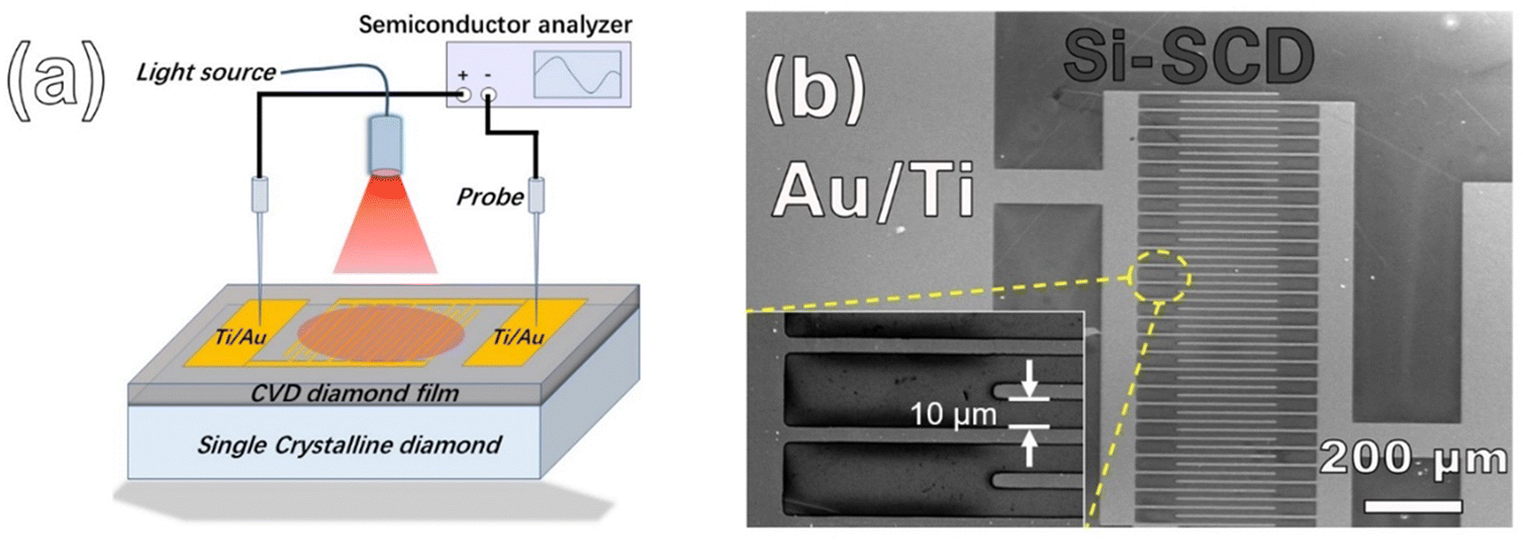 | ||
| Fig. 1 A schematic diagram (a) and SEM image (b) of the Si-doped SCD photodetector with planar interdigital electrodes. | ||
3. Results and discussion
Fig. 2(a) shows planar optical and SEM images of the as-deposited Si-SCD samples, a flat and smooth crystal surface without any macroscopic defects can be observed. The epitaxial Si-SCD film with identical deposition parameters for 30 min was used to prepare the cross-sectional TEM sample for characterization of the growth rate and crystalline quality of the samples with long deposition duration, as shown in Fig. 2(b). The epitaxial film of approximately 230 nm in thickness reveals a relatively low growth rate of 460 nm per hour, which is important for ensuring high crystal quality.21 It is estimated that the film deposited for 8 h exhibits a thickness of about 3.68 μm. No crystalline defects such as dislocation or twins are observed in the films. The diffraction spots shown in the inset of the selected area electron diffraction (SAED) pattern indicate a single crystalline nature with two characteristic crystal plane families of {220} and {400}. However, some lattice defects are observed to be located at the interface between the substrate and the epi-layer, as marked by the yellow circles. Their presence may affect the impurity distribution and optical properties of the sample. The AFM measurement in Fig. S1(a) in the ESI† reveals that the surface RMS roughness of the Si-SCD sample is 1.52 nm, close to the undoped SCD substrate. From the Raman spectra (Fig. 2(c)), the Si-SCD exhibits a strong peak centered at 1332.8 cm−1, corresponding to the first-order Raman line of diamond. The absence of the characteristic peaks of sp2-D (1350 cm−1), sp2-G (1580 cm−1) and trans-polyacetylene (TPA, 1510 cm−1) indicate the high crystalline quality of the Si-doped SCD sample.26,27 Moreover, the full width at half maximum (FWHM) of the diamond Raman peak is estimated to be 2.82 cm−1, which is slightly larger than that of the undoped SCD substrate (2.70 cm−1). Such a value is smaller than that of the polycrystalline diamond films (≈5 cm−1) deposited with a lower methane ratio28 and similar to the value of the CVD epitaxial single crystal diamond (FWHM ≈ 2.8 cm−1) reported previously.29 This implies that the diamond phase is crystallized in good quality in the Si-doped SCD sample. The absence of severe deterioration in the crystal quality of the single crystalline diamond is crucial for high-performance optoelectronic devices.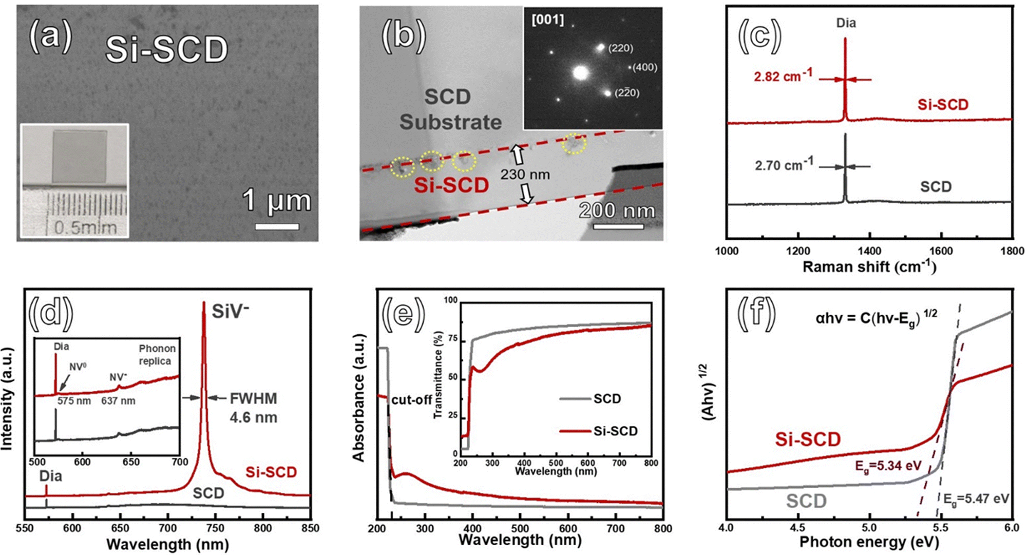 | ||
| Fig. 2 Plan-view SEM image (a) and TEM cross-section image (b) of the Si-doped SCD sample. Room temperature Raman spectra (c), PL spectra (d), UV-vis absorption/transmittance spectra (e) and the corresponding Tauc plot (f) of the samples. | ||
The room temperature PL spectrum of the Si-doped SCD sample is demonstrated in Fig. 2(d). Compared to the SCD sample, the Si-doped SCD sample shows a sharp peak centered at 738 nm along with a sideband at 757 nm, which are assigned to be zero phonon line (ZPL) and phonon replica of negatively charged SiV− centers.30 It is noted that the SiV peak intensity is about 10 times higher than that of the diamond Raman peak (572.6 nm), This suggests that Si atoms have been successfully doped into the epitaxial layer of SCD and participated in the formation of high-brightness SiV centers. The FWHM of the SiV− ZPL is estimated to be about 4.6 nm according to the peak de-convolution procedure using Gauss–Lorentz fitting, similar to that of the reported single-crystal diamond (4.5–5.4 nm).31 This means that small local stress is generated in the Si-SCD epitaxial layer. One explanation is the introduction of Si atoms in the diamond lattice does not give rise to remarkable internal stress compared to that induced by the mismatch in the lattice constant and thermal expansion for hetero-grown diamond films on foreign substrates.32 In addition, an NV0 peak centered at 575 nm and an NV− peak centered at 637 nm is also observed in the Si-doped SCD sample (the inset in Fig. 2(d)).33
According to the UV-vis absorption spectra shown in Fig. 2(e), the Si-doped SCD sample shows a UV cut-off edge at 227 nm with a wide absorption band from the UV to the visible region. In contrast, the SCD sample has an increased intrinsic absorption with a lower absorption band in the visible range. Considering that the Si-doped SCD sample has high crystal quality without any macroscopic defects, the visible absorption band may be caused by the introduction of SiV and NV centers. Correspondingly, the transmittance curves of the inset (Fig. 2(e)) show a lower transparency at the visible region for the Si-doped SCD sample compared to the SCD sample. Moreover, the bandgap (Eg) can be fitted by the Tauc equation:
| (αhν)n = C(hν − Eg) |
Generally, low dark current is very favorable for the performance of a photodetector,35,36 and this current can be effectively tuned by surface termination of diamond. Fig. 3(a) shows the dark current (ID) of the photodetectors for Si-SCD after different surface terminal modifications. It is noted that the H-terminated SCD (H-SCD) exhibits the highest ID value of about 92.5 mA at 15 V bias voltage. Considering that the effective area between the interdigital electrodes is about 0.003 cm,2 the calculated surface resistivity is about 5.41 × 10⁴ Ω cm−2. The high conductivity of H-SCD may be attributed to its two-dimensional hole gas (2-DHG) on the surface acting as a conductive channel.37 When the treatments of acid oxidation (black curve) and annealing in the air (red curve) were conducted sequentially, the dark currents for the O-terminated SCD (O-SCD) samples decreased significantly. It is only about 5.66 × 10⁻¹² A in the air annealed sample, nearly 1010 times lower than the H-SCD. The surface resistivity is calculated to be R ≈ 8.83 × 10¹⁴ Ω cm−2. The variation in surface conductivity with different surface terminations is caused by the variation in carrier concentration.38 The effect of surface modification on carrier concentration is explained by the energy band structure (Fig. 3(b)), where the work functions and the electron affinities can be determined using Kelvin probe force microscopy (KPFM) and ultraviolet photoelectron spectroscopy (UPS) techniques, as shown in Fig. S1 and S2 in the ESI.† The work functions of the H-SCD and O-SCD samples are measured to be 4.85 and 4.27 eV, respectively. The H-SCD sample exhibits a negative electron affinity, which is much smaller than the positive electron affinity for the O-SCD sample. As a result, the Fermi level is located close to the valence band for the H-SCD sample, corresponding to p-type conductivity at the surface of H-SCD, which provides a high concentration of hole for surface conductivity. In comparison, the air-annealed O-SCD sample exhibits a nearly intrinsic conductivity at the surface. Therefore, to obtain high performance of the photodetector, photoelectric measurement is conducted on the oxygen-terminated diamond treated by air annealing in the following section.
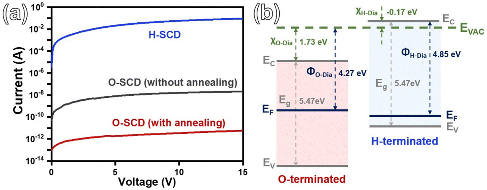 | ||
| Fig. 3 (a) Dark current of the Si-doped SCD sample with different surface terminals (the grey curve represents the original Si-doped simple with weak oxygen terminal without air annealing). (b) The energy band structures of the diamond terminated with oxygen and hydrogen. | ||
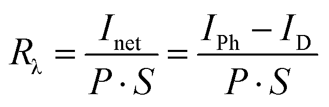
The photocurrent (IPh) of the Si-doped diamond sample with oxygen termination was measured under light illumination of different wavelengths, as shown in the multicolor curves in Fig. 4(a) and (b). The photocurrent of the Si-doped diamond sample is increased with the bias and reaches saturation at 15 V for all the wavelengths. An extremely high saturation IPh of 3.58 × 10⁻⁸ A was generated at a UV wavelength of 220 nm, which is attributed to its stronger absorption of intrinsic excitation below 227 nm. Such a value is slightly lower than the intrinsic excitation of the undoped SCD sample (4.63 × 10⁻⁸ A). This implies that the introduction of SiV centers does not lead to a severe deterioration in device response to solar blind signals. The optical on–off ratio (IPh/ID) of the Si-doped diamond device at 15 V bias is calculated to be approximately 6.33 × 10³, which is about one-quarter the ratio of the SCD (2.92 × 10⁴). In addition, it is observed that the IPh values of the Si-doped diamond device under different near-ultraviolet (254 nm and 365 nm) and visible (400 nm, 450 nm, 532 nm, and 650 nm) irradiations are smaller than the intrinsic excitation under 220 nm. However, the IPh at the above-mentioned light sources for the Si-doped diamond device is larger than that for the undoped substrate, which is caused by its wide absorption band from 250 to 800 nm (red curve in Fig. 2(d)). To further evaluate the device performance, their responsivities (R) to light of different wavelengths are calculated according to the following equation:
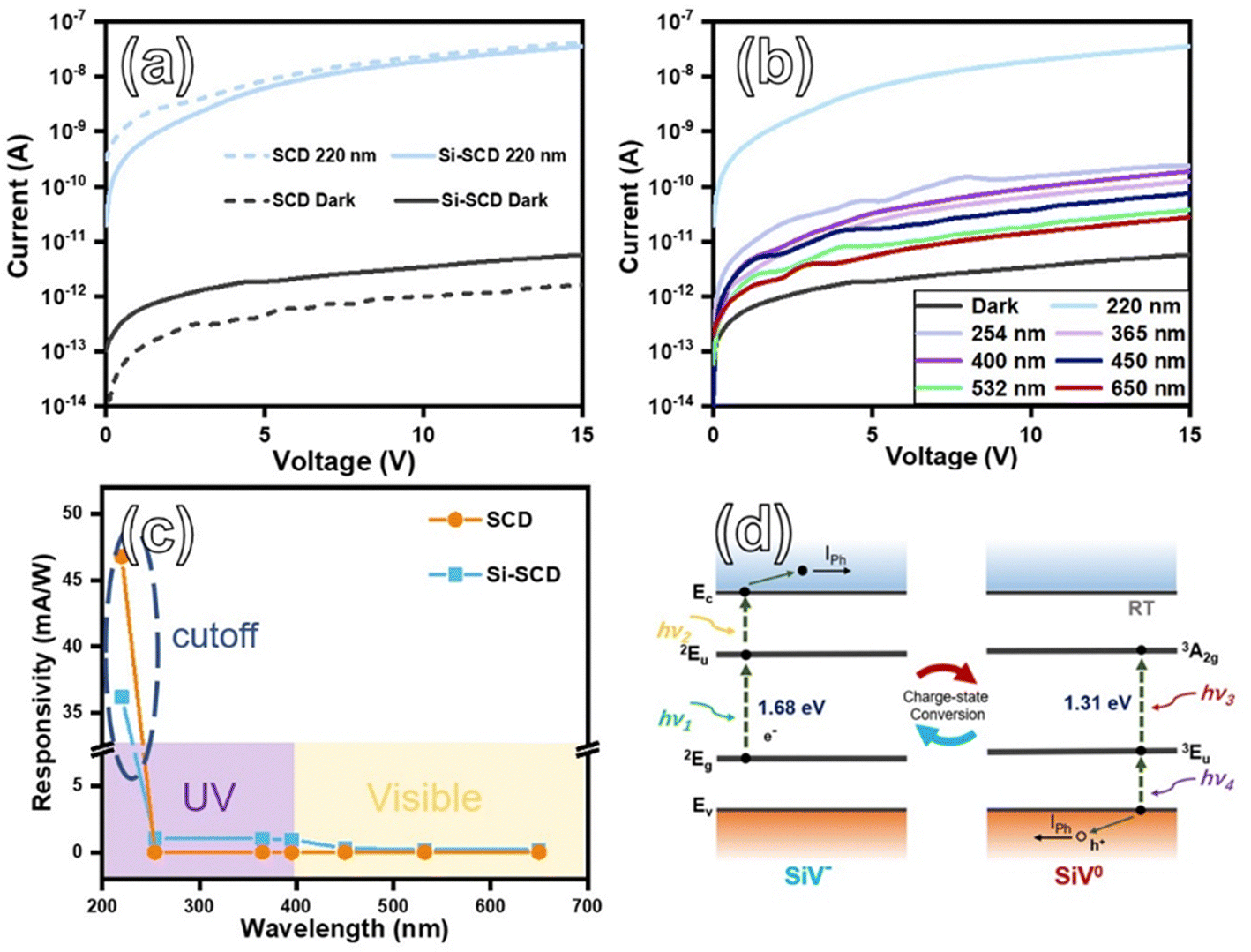 | ||
| Fig. 4 (a) Dark currents (grey curves) and 220 nm intrinsic photocurrents (blue curves) of the SCD and Si-SCD devices. (b) Photocurrent of the Si-SCD device (colored curves) at illuminations of different wavelengths. (c) The device's responsivities to light illumination of different wavelengths. (d) A schematic of carrier transport during the photoionization processes of the SiV centers. | ||
The UV/visible rejection ratio (R220/R400) and detectivity 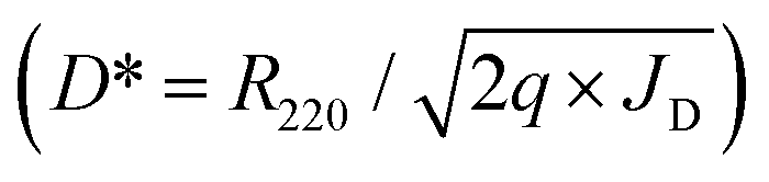 are calculated to evaluate the optical selectivity and sensitivity of the devices. Here, R220 and R400 are the responsibilities of the devices under 220 nm and 400 nm illuminations, respectively. The q is the elementary charge, which equals 1.6 × 10⁻¹⁹ C and the JD is the dark current density. The results are shown in Table 1. The rejection ratio of the Si-SCD device is estimated to be 140, which is much lower than that of the undoped diamond device (78400). However, the detectivity of the Si-doped SCD device is estimated to be 2.10 × 10¹² jones, which is slightly lower than that of the undoped diamond device (5.26 × 10¹² jones). This value is close to that of an all-carbon diamond photodetector using graphite interdigital electrodes (D* = 1.39 × 10¹² jones),41 but much higher than the D* of detector based on a TiO2/diamond heterostructure (D* = 6.57 × 10¹⁰ jones).42 The above results show that the planar Si-doped diamond photodetectors prepared in this work demonstrate high detection rates for deep UV wavelength.
| Device | ID (A) | On–off ratio | R (mA W−1) | RUV/RVis | D* (jones) | trise/tdecay (s) | Ref. |
|---|---|---|---|---|---|---|---|
| Si-SCD | 5.66 × 10⁻¹² | 6.33 × 10³ | 36.2 | 140 | 2.10 × 10¹² | 1.27/0.53 | In this work |
| SCD | 1.1 × 10⁻¹² | 1 × 10⁴ | 48.0 | 1 × 10⁴ | — | ∼80/— | 29 |
| SCD | 3.68 × 10⁻¹³ | 20.8 | 7.86 | ∼50 | — | — | 43 |
| B-SCD/Al | 1.0 × 10⁻¹² | ∼10 | 28.0 | 1 × 10³ | — | — | 44 |
| SCD/TiO2 | 1.12 × 10⁻¹² | 6.7 × 10⁷ | 200 | 1 × 10⁵ | 6.57 × 10¹⁰ | 2 × 10⁻⁵/1 × 10−3 | 42 |
| SCD/Gr | 5 × 10⁻⁶ | ∼120 | 21800 |
8.9 × 10³ | 1.39 × 10¹² | 3.1 × 10⁻⁴/3.3 × 10−4 | 41 |
Fig. 5(a)–(d) shows the time-resolved photocurrent of the devices under 15 V bias and 220 nm illumination. It can be seen that the current of the two devices can be reversibly modulated with light illumination (Fig. 5(a) and (b)), exhibiting high stability and repeatability, which is crucial for applications in communication systems.45 The rise (trise) and decay (tdecay) periods of IPh are generally defined as the response time required for the photocurrent to change from 10% to 90% of the maximum value. Accordingly, the trise values of the undoped and the Si-SCD devices are estimated to be 0.95 s and 1.27 s, respectively. This implies that the introduction of Si dopant prolongs the trise by about 1/3. The time resolved photoluminescence (TRPL) measurement (Fig. S3, ESI†) has been applied to study the lifetime of photoinduced carriers in both the samples, the average lifetime of the Si-SCD and the SCD is 3.80 and 4.50 ns, respectively. This indicates a higher defect density in the Si-doped sample, which may lead to a trapping effect and prolong the response time of photocurrent. On the other hand, the corresponding tdecay of the two devices is 0.65 s and 0.53 s (Fig. 5(c) and (d)), implying the shorter lifetime of the non-equilibrium carriers. The Si-doped SCD devices exhibit a faster response during the photocurrent decaying stage, suggesting that the carriers in the Si-SCD detector recombine more rapidly upon the shutdown of light illumination. Generally, the shorter lifetime usually derives from Shockley–Read–Hall (SRH) recombination,46 while the longer lifetime could be attributed to the de-trapping of carriers at defects.47 In our work, it is believed that the existence of SiV defects further promotes carrier recombination and reduces the decay time, which is beneficial for achieving a fast cut-off of photodetectors. A comparison with the reported parameters of diamond-based photodetectors is listed in Table 1. Our devices exhibit relatively high detectivity to solar blind signals as well as an ideal on–off ratio compared to most of the devices reported previously.29,41–44 Hence, for single crystal diamond photodetectors, the introduction of SiV centers does not lead to a significant deterioration of their intrinsic performance and meanwhile promotes its response to near-ultraviolet and visible signals.
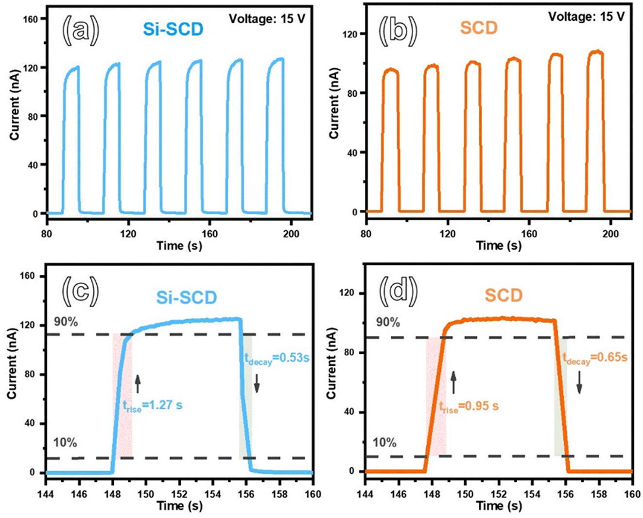 | ||
| Fig. 5 Time-resolved photocurrent of the Si-doped (a) and (c) and the undoped (b) and (d) SCD detectors. | ||
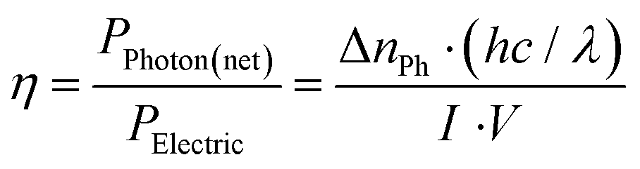
In addition to the inflorescent SRH recombination, fluorescent recombination of charge carriers also occurs during their separation at external bias, which will vary the PL emission of color centers. The electrically pumped PL spectra of SiV centers were recorded at the diamond region close to the electrode using a Raman spectrometer (532-nm laser) with a high-precision DC power supply, as shown in Fig. 6(a). For a clearer comparison, the results are normalized by the diamond Raman peak at 572.6 nm. The inset shows the CCD optical image during testing with the laser spot size of approximately 1 μm (d = 1.22λ/NA), which is much smaller than the interdigital electrode spacing (10 μm). The results show that the PL of SiV− (738 nm) significantly increases with bias voltage, namely, the radiative recombination of injected carriers occurs at SiV defects and enhances its PL emission. This is consistent with our previous work,48 where a similar PL variation also appears for polycrystalline diamond/heavy-doped n-type Si vertical heterostructure (Dia/n+-Si) under the electrical pump. Fig. 6(b) shows the normalized PL intensity of the Si-doped SCD device. It can be seen that the PL of the Si-SCD device increases by 50% at 60 V bias, which is slower than the PL enhancement for the Dia/n+-Si heterostructure (90% at 50 V), owing to the higher injection current for forward-biased diode and wider tailoring region for vertical structure. For further evaluation, the electrical enhancement efficiency (η) is defined as the power of the net number of emitted photons divided by the power of injected carriers, as shown in the equation below:
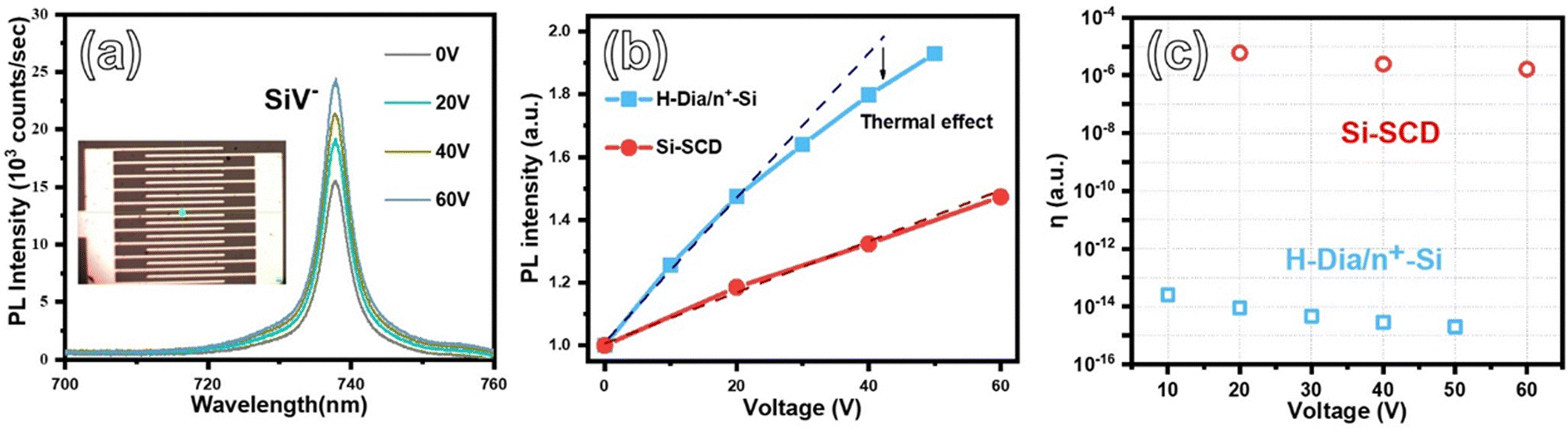 | ||
| Fig. 6 (a) PL spectra (532 nm laser) of the Si-doped SCD device at different bias voltages. The normalized SiV− PL variation (b) and the calculated electrical enhancement efficiency at different bias voltages (c). | ||
4. Conclusions
In this work, a high quality silicon-doped single crystal diamond photodetector was prepared by MPCVD and photolithography techniques. High-brightness SiV centers are introduced with slightly deteriorating the crystal quality. The Si-doped photodetector with oxygen termination exhibits a responsivity of 36.2 mA W−1 with detectivities of 2.10 × 10¹² jones at 220-nm illumination, implying that the introduction of the SiV centers will not significantly reduce the intrinsic response of diamond. Owing to the SiV center, the Si-doped photodetector exhibits a near-UV/visible responsivity of 102 to 103 times higher than that of the undoped photodetector. Additionally, a faster cut-off speed is realized for the Si-doped photodetector, which is attributed to the photoionization of SiV defects and the SRH recombination of photogenerated carriers. In addition, a 50% PL enhancement of SiV centers was achieved for the Si-doped photodetector by applying an external electrical field, which originates from the radiative combination of photo-induced charge carriers. The single-crystalline diamond device exhibits 109 times electrical enhancement efficiency for SiV PL emission compared to the polycrystalline diamond devices, also making it a potential candidate for applications as a room temperature single photon source.Author contributions
Xiaokun Guo: conceptualization, data curation, formal analysis, investigation, methodology, visualization, validation, writing – original draft and writing – review & editing. Bing Yang: conceptualization, formal analysis, funding acquisition, project administration, resources, supervision and writing – review & editing. Xinglai Zhang: formal analysis, resources and methodology. Jiaqi Lu: data curation, formal analysis and methodology. Ming Huang: data curation, formal analysis and resources. Nan Huang: project administration and resources. Lusheng Liu: resources and supervision. Xin Jiang: funding acquisition, project administration, resources and supervision.Data availability
The data supporting this article have been included as part of the ESI.†Conflicts of interest
There are no conflicts to declare.Acknowledgements
B. Y. would like to thank the National Natural Science Foundation of China (Grants No. 52172056) and the National Natural Science Foundation from Liaoning province (No. 2022MS009) for financial support.Notes and references
- Y. Lu, C. Lin and C. Shan, Adv. Opt. Mater., 2018, 6, 1800359 CrossRef.
- C. Xie, X. Lu, X. Tong, Z. Zhang, F. Liang, L. Liang, L. Luo and Y. Wu, Adv. Funct. Mater., 2019, 29, 1806006 CrossRef.
- H. Chen, H. Liu, Z. Zhang, K. Hu and X. Fang, Adv. Mater., 2016, 28, 403–433 CrossRef CAS PubMed.
- Z. Zhang, C. Lin, X. Yang, J. Zang, K. Li, Y. Lu, Y. Li, L. Dong and C. Shan, J. Mater. Chem. C, 2022, 10, 6488–6496 RSC.
- U. F. Ahmad, Y. S. Wudil, A. Imam, N. F. Isa, M. A. Gondal and M. A. Al-Osta, Mater. Today Commun., 2023, 36, 106409 CrossRef CAS.
- Y. Chen, Y. Lu, C. Lin, Y. Tian, C. J. Gao, L. Dong and C. Shan, J. Mater. Chem. C, 2018, 6, 5727–5732 RSC.
- M. Wei, K. Yao, Y. Liu, C. Yang, X. Zang and L. Lin, Small, 2017, 13, 1701328 CrossRef PubMed.
- R. Rao, C. L. Pint, A. E. Islam, R. S. Weatherup, S. Hofmann, E. R. Meshot, F. Wu, C. Zhou, N. Dee, P. B. Amama, J. C.-Nuñez, W. Shi, D. L. Plata, E. S. Penev, B. I. Yakobson, P. B. Balbuena, C. Bichara, D. N. Futaba, S. Noda, H. Shin, K. S. Kim, B. Simard, F. Mirri, M. Pasquali, F. Fornasiero, E. I. Kauppinen, M. Arnold, B. A. Cola, P. Nikolaev, S. Arepalli, H. Cheng, D. N. Zakharov, E. A. Stach, J. Zhang, F. Wei, M. Terrones, D. B. Geohegan, B. Maruyama, S. Maruyama, Y. Li, W. W. Adams and A. J. Hart, ACS Nano, 2018, 12, 11756–11784 CrossRef CAS PubMed.
- A. F. Zhou, R. Velazquez, X. Wang and P. X. Feng, ACS Appl. Mater. Interfaces, 2019, 11, 38068–38074 CrossRef CAS PubMed.
- P. Neumann, I. Jakobi, F. Dolde, C. Burk, R. Reuter, G. Waldherr, J. Honert, T. Wolf, A. Brunner, J. H. Shim, D. Suter, H. Sumiya, J. Isoya and J. Wrachtrup, Nano Lett., 2013, 13, 2738–2742 CrossRef CAS PubMed.
- C. Bradac, W. Gao, J. Forneris, M. E. Trusheim and I. Aharonovich, Nat. Commun., 2019, 10, 5625 CrossRef CAS PubMed.
- B. C. Rose, D. Huang, Z. H. Zhang, P. Stevenson, A. M. Tyryshkin, S. Sangtawesin, S. Srinivasan1, L. Loudin, M. L. Markham, A. M. Edmonds, D. J. Twitchen, S. A. Lyon and N. P. De Leon, Science, 2018, 361, 60–63 CrossRef CAS PubMed.
- F. Dolde, I. Jakobi, B. Naydenov, N. Zhao, S. Pezzagna, C. Trautmann, J. Meijer, P. Neumann, F. Jelezko and J. Wrachtrup, Nat. Phys., 2013, 9, 139–143 Search PubMed.
- P. Sittimart, S. Ohmagari, H. Umezawa, H. Kato, K. Ishiji and T. Yoshitake, Adv. Opt. Mater., 2023, 11, 2203006 Search PubMed.
- F. M. Hrubesch, G. Braunbeck, M. Stutzmann, F. Reinhard and M. S. Brandt, Phys. Rev. Lett., 2017, 118, 037601 CrossRef PubMed.
- P. Siyushev, M. Nesladek, E. Bourgeois, M. Gulka, J. Hruby, T. Yamamoto, M. Trupke, T. Teraji, J. Isoyaand and F. J. Agio, Science, 2019, 363, 728–731 CrossRef CAS PubMed.
- E. Bourgeois, M. Gulka and M. Nesladek, Adv. Opt. Mater., 2020, 8, 1902132 CrossRef CAS.
- C. L. Smallwood, R. Ulbricht, M. W. Day, T. Schröder, K. M. Bates, T. M. Autry, G. Diederich, E. Bielejec, M. E. Siemens and S. T. Cundiff, Phys. Rev. Lett., 2021, 126, 213601 CrossRef CAS PubMed.
- L. Ondic, M. Varga, K. Hruška, J. Fait and P. Kapusta, ACS Nano, 2017, 11, 2972–2981 CrossRef CAS PubMed.
- M. A. Lobaev, A. M. Gorbachev, D. B. Radishev, A. L. Vikharev, S. A. Bogdanov, V. A. Isaev and M. N. Drozdov, J. Mater. Chem. C, 2021, 9, 9229–9235 RSC.
- B. Yang, J. Li, L. Guo, N. Huang, L. Liu, Z. Zhai, W. Long and X. Jiang, CrystEngComm, 2018, 20, 1158–1167 RSC.
- J. Lu, B. Yang, B. Yu, H. Li, N. Huang, L. Liu and X. Jiang, Adv. Opt. Mater., 2021, 9, 2101427 CrossRef CAS.
- B. Yang, B. Yu, H. Li, N. Huang, L. Liu and X. Jiang, Carbon, 2020, 156, 242–252 CrossRef CAS.
- B. Yu, B. Yang, H. Li, J. Lu, N. Huang, L. Liu and X. Jiang, Appl. Surf. Sci., 2021, 552, 149475 CrossRef CAS.
- P. E. Viljoen, E. S. Lambers and P. H. Holloway, J. Vac. Sci. Technol., B, 1994, 12, 2997–3005 CrossRef CAS.
- S. Osswald, G. Yushin, V. Mochalin, S. O. Kucheyev and Y. Gogotsi, J. Am. Chem. Soc., 2006, 128, 11635–11642 CrossRef CAS PubMed.
- A. C. Ferrari and J. Robertson, Phys. Rev. B: Condens. Matter Mater. Phys., 2001, 63, 121405 CrossRef.
- X. Jiang, C. P. Klages, R. Zachai, M. Hartweg and H. J. Füsser, Appl. Phys. Lett., 1993, 62, 3438–3440 CrossRef CAS.
- A. BenMoussa, A. Soltani, K. Haenen, U. Kroth, V. Mortet, H. A. Barkad, D. Bolsee, C. Hermans, M. Richter and J. C. De Jaeger, Semicond. Sci. Tech., 2008, 23, 035026 CrossRef.
- A. Dietrich, K. D. Jahnke, J. M. Binder, T. Teraji, J. Isoya, L. J. Rogers and F. Jelezko, New J. Phys., 2014, 16, 113019 CrossRef.
- S. Choi, V. N. Agafonov, V. A. Davydov and T. Plakhotnik, ACS Photonics, 2019, 6, 1387–1392 CrossRef CAS.
- B. Andrey, R. Victor, S. Vadim, K. Andrey, V. Igor, K. Alexander, T. Nikolay, K. Vladimir, N. Sergei, K. Roman and S. Vladimir, Phys. Status Solidi A, 2015, 212, 2525–2532 CrossRef.
- C. Schreyvogel, M. Wolfer, H. Kato, M. Schreck and C. E. Nebel, Sci. Rep., 2014, 4, 3634 CrossRef PubMed.
- Y. Wang, J. Su, Z. Lin, J. Zhang, J. Chang and Y. Hao, J. Mater. Chem. C, 2022, 10, 13395–13436 RSC.
- G. Simone, M. J. Dyson, S. C. Meskers, R. A. Janssen and G. H. Gelinck, Adv. Funct. Mater., 2020, 30, 1904205 CrossRef CAS.
- N. Youngblood, C. Chen, S. J. Koester and M. Li, Nat. Photon., 2015, 9, 247–252 CrossRef CAS.
- Y. Sasama, T. Kageura, M. Imura, K. Watanabe, T. Taniguchi, T. Uchihashi and Y. Takahide, Nat. Electron., 2022, 5, 37–44 CrossRef CAS.
- J. Raymakers, K. Haenen and W. Maes, J. Mater. Chem. C, 2019, 7, 10134–10165 RSC.
- T. Murooka, M. Shiigai, Y. Hironaka, T. Tsuji, B. Yang, T. M. Hoang, K. Suda, K. Mizuno, H. Kato, T. Makino, M. Ogura, S. Yamasaki, M. Hatano and T. Iwasaki, Appl. Phys. Lett., 2021, 118, 253502 CrossRef CAS.
- C. Hepp, T. Müller, V. Waselowski, J. N. Becker, B. Pingault, H. Sternschulte, D. Steinmüller-Nethl, A. Gali, J. R. Maze, M. Atatüre and C. Becher, Phys. Rev. Lett., 2014, 112, 036405 CrossRef PubMed.
- C. Lin, Y. Lu, X. Yang, Y. Tian, C. Gao, J. Sun, L. Dong, F. Zhong, W. Hu and C. Shan, Adv. Opt. Mater., 2018, 6, 1800068 CrossRef.
- Z. Liu, F. Li, S. Li, C. Hu, W. Wang, F. Wang, F. Lin and H. Wang, Sci. Rep., 2015, 5, 14420 CrossRef CAS PubMed.
- Z. C. Liu, F. N. Li, W. Wang, J. W. Zhang, F. Lin and H. X. Wang, MRS Adv., 2016, 1, 1099–1104 CrossRef CAS.
- X. Shi, Z. Yang, S. Yin and H. Zeng, Mater. Technol., 2016, 31, 544–547 CrossRef CAS.
- C. Lin, Y. Lu, Y. Tian, C. Gao, M. Fan, X. Yang, L. Dong and C. Shan, Opt. Express, 2019, 27, 29962–29971 CrossRef CAS PubMed.
- J. Chen and N. G. Park, Adv. Mater., 2019, 31, 1803019 CrossRef CAS PubMed.
- Z. Fan, H. Fan, L. Yang, P. Li, Z. Lu, G. Tian, Z. Huang, Z. Li, J. Yao, Q. Luo, C. Chen, D. Chen, Z. Yan, M. Zeng, X. Lu, X. Gao and J. M. Liu, J. Mater. Chem. C, 2017, 5, 7317–7327 RSC.
- X. Guo, B. Yang, J. Lu, H. Li, N. Huang, L. Liu and X. Jiang, J. Mater. Chem. C, 2022, 10, 9334–9343 RSC.
Footnote |
| † Electronic supplementary information (ESI) available. See DOI: https://doi.org/10.1039/d4tc02335h |
| This journal is © The Royal Society of Chemistry 2024 |