
Ternary solar cells with a mixed face-on and edge-on orientation enable an unprecedented efficiency of 12.1%†
Tanya
Kumari‡
,
Sang Myeon
Lee‡
,
So-Huei
Kang
,
Shanshan
Chen
and
Changduk
Yang
*
Department of Energy Engineering, School of Energy and Chemical Engineering, Perovtronics Research Center, Low Dimensional Carbon Materials Center, Ulsan National Institute of Science and Technology (UNIST), 50 UNIST-gil, Ulju-gun, Ulsan 44919, South Korea. E-mail: yang@unist.ac.kr
First published on 11th November 2016
Abstract
Ternary organic solar cells (OSCs), with a simple structure, can be easily adopted as sub-cells in a tandem design, thereby further enhancing the power conversion efficiency (PCE). Considering the potential to surpass the theoretical PCE limit in OSCs, we incorporated a benzo[1,2-b;4,5-b′]dithiophene-based small molecule into a poly(4,8-bis(5-(2-ethylhexyl)thiophen-2-yl)benzo[1,2-b;4,5-b′]dithiophene-2,6-diyl-alt-(4-(2-ethylhexyl)-3-fluorothieno[3,4-b]thiophene-)-2-carboxylate-2-6-diyl):[6,6]-phenyl-C71-butyric acid methyl ester host system. A hitherto unrealized PCE of 12.1% was achieved at the optimized composition of the ternary blend. The ternary blend surprisingly had a face-on and edge-on co-existent texture, which is far better than that of the face-on orientated host film. To the best of our knowledge, this intriguing result refutes for the first time a general paradigm that high-performance OSCs are unambiguously linked to face-on structures. Therefore, our study provides a new platform for refining the theoretical underpinning of multiple blending OSCs.
Broader contextWith enormous research interest in the past few years, ternary blend organic solar cells (OSCs) comprising multiple donor or acceptor materials in an active layer have emerged as promising alternatives to enhance photovoltaic parameters for spectrally broad light harvesting while retaining the simplicity of a single step for processing the active layer as compared with traditional binary or tandem OSCs. Recent ternary structures of conjugated polymers have achieved around 10% power conversion efficiencies (PCEs), showing the great potential of ternary systems. Herein, we report ternary OSCs fabricated by incorporating DR3TSBDT as an additional donor into a PTB7-Th:PC71BM host matrix at different weight ratios, exhibiting the record-PCE of 12.1% under highly optimized conditions. Through a series of characterization techniques, we identified that our ternary OSCs have mixed face-on and edge-on orientations, reaching much improved PCEs unlike common high-performing OSCs that preferentially favor face-on orientated host systems. Additionally, our study reveals that the exceptionally high PCE in this ternary structure results from not only improving the photon absorption range but also facilitating charge transport while reducing recombination. This is achieved through a combination of cascade energy levels and optimized morphology. |
Introduction
An in-depth understanding of the operating mechanism of binary blend organic solar cells (OSCs), consisting of a polymeric donor and a fullerene acceptor, has enabled several research efforts aimed at increasing the power conversion efficiencies (PCEs) of OSCs.1–4 An optimization process involving a synergistic combination of active material design,2,5,6 nanoscale morphology control,7–9 and device engineering10–12 resulted in a significant breakthrough of over 10% PCEs for single-junction binary OSCs.3,4,13–16 In a promising approach for further increasing the PCEs, tandem OSCs – in which two (or more) sub-cells absorbing light in different regions of the solar spectrum are connected in either series or parallel – have been studied.17,18 The impressive progress in the field of tandem OSCs has laid a solid foundation for improving the PCEs by ∼40–50%,19,20 demonstrating their immense potential for a practically realizable OSC technology. Nonetheless, there are several drawbacks in using tandem architectures, such as the complex fabrication process and high production cost, which limits their practical application.17,21Ternary blend OSCs comprising two donors and one acceptor (or one donor and two acceptors) are emerging as a fascinating alternative to overcome the challenges encountered during spectrally broad light harvesting using multi-junction OSC processing while retaining the simplicity of single-step processing of the active layer.14,22–25 Despite some successful examples of ternary OSCs achieved by carefully selecting multiple components,7,26–32 the current PCEs generally continue to be far less than the state-of-the-art binary and tandem systems. This is because the third component within the host binary systems can act as a recombination center or a morphological trap rather than a control agent to extend the absorption of the solar spectrum, since unfavourable interactions between the third component and host blend are inevitable.33,34 Therefore, the molecular compatibility of the active materials used in ternary OSCs is believed to be critical in achieving high PCEs.3,14,35–41 We speculate that in a vast pool of available active materials, the use of an archetype of the high-performance poly(4,8-bis(5-(2-ethylhexyl)thiophen-2-yl)benzo[1,2-b;4,5-b′]dithiophene-2,6-diyl-alt-(4-(2-ethylhexyl)-3-fluorothieno[3,4-b]thiophene-)-2-carboxylate-2-6-diyl) (PTB7-Th):[6,6]-phenyl-C71-butyric acid methyl ester (PC71BM) binary host can pave a shortcut for discovering ideal ternary systems. In addition to its appropriate energy level alignment and high-crystalline characteristics, a benzo[1,2-b;4,5-b′]dithiophene (BDT)-based small molecule, namely DR3TSBDT, is intuitively expected to have good compatibility with PTB7-Th because of the molecular similarity in their backbones, which is based on identical BDT units.
Given this background, a ternary OSC was designed and fabricated by incorporating DR3TSBDT as the additional donor into the PTB7-Th:PC71BM host matrix. The ternary system demonstrated an unprecedented PCE of 12.1% under optimal conditions. Unlike common high-performance OSCs that favour a face-on orientation, our ternary OSCs have a mixed orientation, which is a combination of face-on and edge-on orientations, thus enabling much higher PCEs compared to the preferentially face-on orientated host system. Our in-depth study reveals that the exceptionally high PCE results from not only improving the photon absorption range but also facilitating charge transport while reducing recombination. This is achieved through a combination of cascade energy levels and optimized morphology.
Results and discussion
Characterization and optical properties
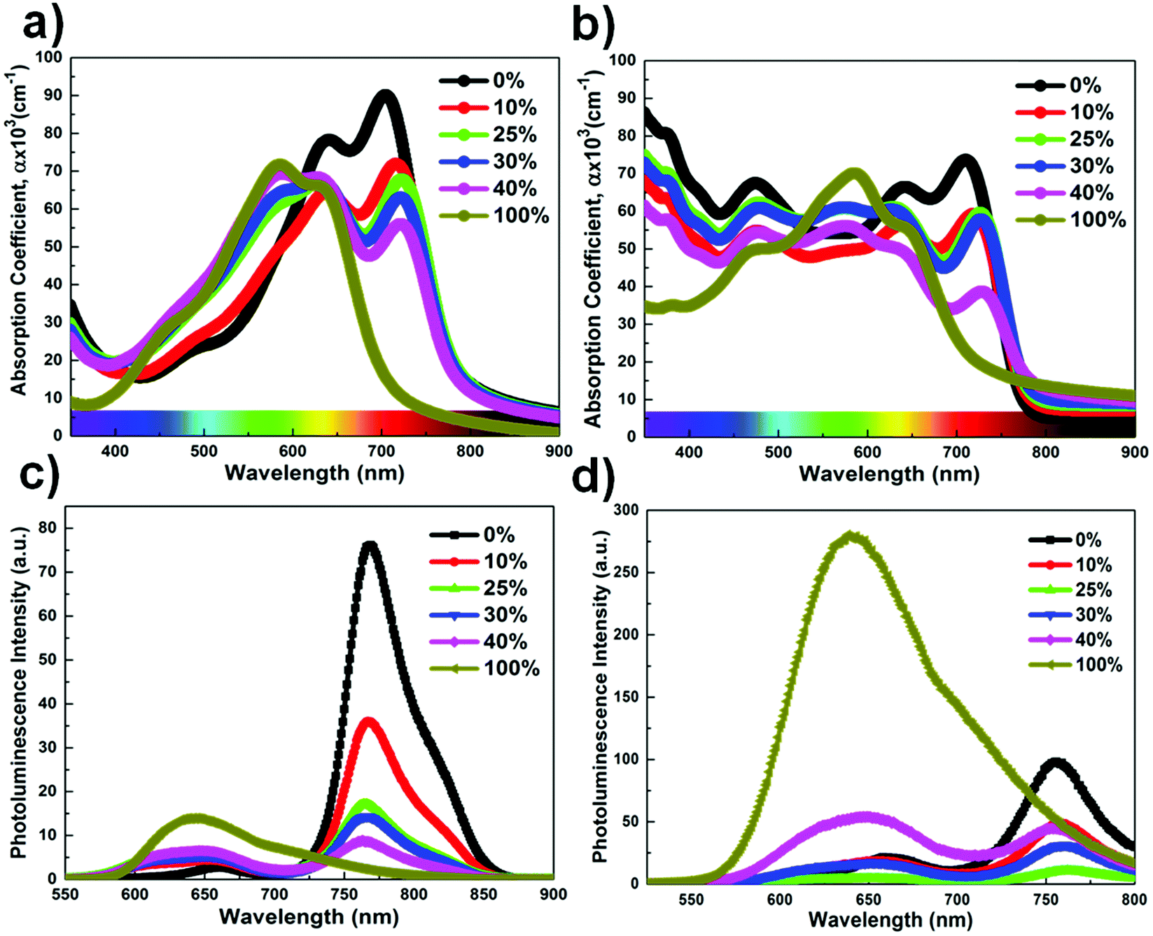
The chemical structures of PTB7-Th, DR3TSBDT, and PC71BM, as well as the device architecture and corresponding energy levels, are given in Fig. 1a and b. We first carried out a detailed spectroscopy study to understand the changes in the chlorobenzene (CB) solution and in the chlorobenzene based thin film following the incorporation of the third component. The two donor components exhibit complementary absorption spectra (Fig. 2a and ESI,† Fig. S1a). The maximum absorption for the PTB7-Th film is at 706 nm and that of the DR3TSBDT film is centered at 586 nm. As the DR3TSBDT content in PTB7-Th increased, the absorption intensity gradually increased in the region of 400–600 nm, while the absorption at around 700 nm decreased. Note that the maximum absorption of PTB7-Th is red-shifted following the incorporation of DR3TSBDT. Fig. 2b shows the effect of incorporating various concentrations of DR3TSBDT into the PTB7-Th![[thin space (1/6-em)]](https://www.rsc.org/images/entities/char_2009.gif) :PC71BM host at a certain blending ratio (1:1.5 wt/wt). As for the absorption spectra of the two donor mixtures (Fig. 2a), it is seen that incorporating DR3TSBDT to form ternary blends leads to a small red-shift in the low-energy absorption band, implying an increased molecular ordering in PTB7-Th, which is induced by the favourable interaction with DR3TSBDT. Therefore, we expect that an optimal amount of DR3TSBDT will facilitate the crystallization of PTB7-Th in ternary OSCs. In addition, the ternary films formed using 10–30 wt% DR3TSBDT provide relatively high absorption intensity over a broad wavelength range of 300 to 800 nm (Fig. 2b).
:PC71BM host at a certain blending ratio (1:1.5 wt/wt). As for the absorption spectra of the two donor mixtures (Fig. 2a), it is seen that incorporating DR3TSBDT to form ternary blends leads to a small red-shift in the low-energy absorption band, implying an increased molecular ordering in PTB7-Th, which is induced by the favourable interaction with DR3TSBDT. Therefore, we expect that an optimal amount of DR3TSBDT will facilitate the crystallization of PTB7-Th in ternary OSCs. In addition, the ternary films formed using 10–30 wt% DR3TSBDT provide relatively high absorption intensity over a broad wavelength range of 300 to 800 nm (Fig. 2b).
 | ||
| Fig. 1 (a) Chemical structures of PTB7-Th, DR3TSBDT, and PC71BM. (b) Device architecture with illustration of the active layer morphology in ternary OSCs and an energy level diagram. | ||
 | ||
| Fig. 2 (a) Absorption spectra of two donor blend films. (b) Absorption spectra of ternary blend films. (c) Photoluminescence spectra (PL) of two donor binary blend films. (d) Photoluminescence spectra (PL) of two donor ternary blend films with PC71BM in chlorobenzene solution (excitation at ∼500 nm). | ||
Fig. 2c and d show the photoluminescence (PL) spectra of each neat donor, two-donor binary blends, and ternary blend solutions under excitation at ∼500 nm. PTB7-Th exhibits a rather structured emission with a maximum at 760 nm and DR3TSBDT shows a broad emission peak from 580 to 800 nm, which overlaps with the absorption spectrum of PTB7-Th. A gradual increase in the emission intensity of DR3TSBDT was observed, while the emission intensity of PTB7-Th decreased with increasing DR3TSBDT loading ratios, reflecting the existence of Förster energy transfer between DR3TSBDT and PTB7-Th.22,25,27,30 Interestingly, the quenching of the emission was more efficient in ternary films with 25 wt% DR3TSBDT than in other ternary blends, implying the feasibility of a relatively optimized charge transfer pathway at the two donor/acceptor interface.
Photovoltaic performance
The photovoltaic performance of OSCs fabricated using different DR3TSBDT concentrations was evaluated using a conventional architecture of indium-tin oxide (ITO)/poly(3,4-ethylenedioxythiophene):poly(styrene sulfonate) (PEDOT:PSS)/active layer/Al under simulated AM 1.5G irradiation (100 mW cm−2). The overall donor to PC71BM ratio in the active layer was fixed at 1:1.5 wt/wt. 1,8-Diiodooctane (DIO, 3.0 vol%) was used as a processing additive. This paper presents a discussion on the representative ternary blend systems (0, 10, 25, 30, 40, and 100 wt% DR3TSBDT loading ratios). Additional details of the ternary blends examined in this study are included in the ESI,† Fig. S2 and S3.
The current density–voltage (J–V) characteristics of the OSCs are shown in Fig. 3a and the corresponding device parameters are summarized in Table 1. Using highly optimized conditions for PTB7-Th:PC71BM binary OSCs, a maximum PCE of 10.10% was obtained, with a short-circuit current density (JSC) of 19.43 ± 0.30 mA cm−2, an open-circuit voltage (VOC) of 0.785 ± 0.004 V, and a fill factor (FF) of 64.90 ± 0.40%. The PCE value reported in this study is comparable with that of the previous best OSCs based on PTB7-Th:PC71BM.25,42 Upon the addition of 25 wt% DR3TSBDT into the host system, the JSC value increases continuously together with a moderate enhancement in the FF (up to 70.44%), whereas a marginal decrease in the VOC value was observed in the range of 0.794–0.772 V. Meanwhile, at DR3TSBDT loadings higher than 30 wt%, a large drop in the JSC value was observed. Therefore, ternary OSCs with a 25 wt% DR3TSBDT content exhibited the best photovoltaic performance with a JSC value of 22.63 ± 0.67 mA cm−2, a VOC value of 0.765 ± 0.007 V, and a FF value of 68.5 ± 1.9%, in an unprecedented PCE of 12.1% (average PCE = 11.78 ± 0.34%). One of our best cells was sent to an independent solar cell calibration laboratory (Nano Convergence Practical Application Center, South Korea) for certification, confirming a PCE of 11.76%, with VOC = 0.756 V, JSC = 23.76 mA cm−2, FF = 65.5% (see the ESI,† Fig. S4), and is detailed in the Experimental section. To the best of our knowledge, this value is among the highest certified PCE reported to date for any type of OSC. Evidence of a hysteresis less J–V characteristic curve for one of the best devices is also provided (ESI,† Fig. S5). Additionally, we observed that VOC is composition-dependent in the blend systems studied, rather than being determined by the difference between the PC71BM LUMO (lowest unoccupied molecular orbital) and the lowest-available donor HOMO (highest occupied molecular orbital) level. The observed behavior in VOC suggests the formation of an alloy-like model induced by the compatible donors.1,3,43
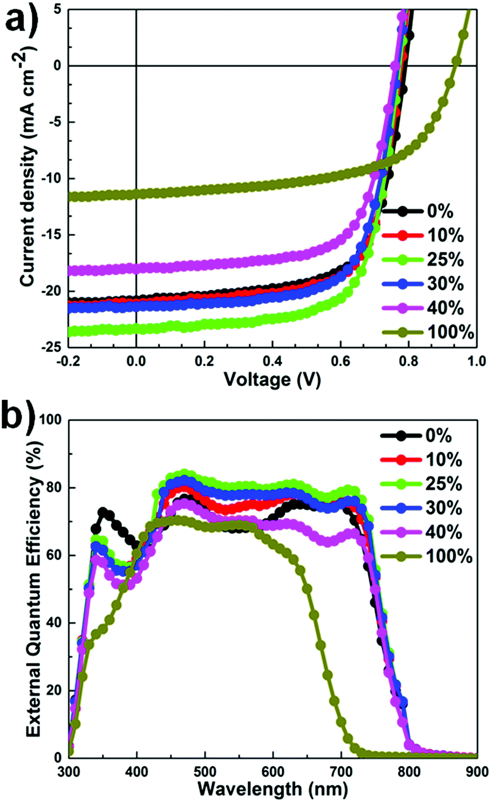 | ||
| Fig. 3 (a) J−V characteristics of OSCs under AM 1.5G irradiation at 100 mW cm−2. (b) The corresponding EQE curves. | ||
| DR3TSBDT ratios | J SC (mA cm−2) | V OC (V) | FFa (%) | PCEa (%) | μ h (cm2 V−1 s−1) | μ e (cm2 V−1 s−1) | μ h/μeb |
|---|---|---|---|---|---|---|---|
| a The average values obtained from at least 16 devices with standard deviation. The data in parentheses are the highest values. b The average values obtained from at least 4 devices with standard deviation. | |||||||
| 0% | 19.43 (19.70) | 0.785 (0.789) | 64.90 (65.30) | 9.87 (10.10) | 1.578 × 10⁻⁴ | 1.066 × 10⁻⁴ | 1.478 |
| 10% | 20.72 (21.69) | 0.772 (0.782) | 67.83 (69.90) | 10.79 (11.30) | 1.683 × 10⁻⁴ | 1.134 × 10⁻⁴ | 1.483 |
| 25% | 22.63 (23.31) | 0.765 (0.772) | 68.51 (70.44) | 11.78 (12.10) | 2.200 × 10⁻⁴ | 1.268 × 10⁻⁴ | 1.735 |
| 30% | 19.90 (21.38) | 0.762 (0.770) | 67.78 (69.30) | 10.97 (11.30) | 2.119 × 10⁻⁴ | 1.176 × 10⁻⁴ | 1.801 |
| 40% | 17.37 (18.00) | 0.756 (0.766) | 67.60 (69.10) | 8.88 (9.26) | 2.020 × 10⁻⁴ | 1.048 × 10⁻⁴ | 1.927 |
| 100% | 12.92 (13.41) | 0.897 (0.902) | 54.80 (56.72) | 4.99 (5.52) | 0.208 × 10⁻⁴ | 0.159 × 10⁻⁴ | 1.309 |
From the differential scanning calorimetry (DSC) data, as shown in the ESI† Fig. S6, the heating curve of the pristine DR3TSBDT shows a clearly endothermic transition (i.e., melting peak), confirming its relatively high crystallinity. In contrast, no such thermally induced transition occurs during the heating cycle of both the pristine PTB7-Th and all the blend systems of PTB7-Th:DR3TSBDT, suggesting a lack of pure DR3TSBDT domains in the blends.3,44,45 Similar surface energies of 28.4 and 30.6 mJ m−2 for DR3TSBDT and the PTB7-Th:PC71BM host blend, respectively, calculated using the Young's equation,46 provide additional proof of the good miscibility in the ternary systems (ESI,† Fig. S7). This was further evidenced using energy dispersive X-ray analysis (EDAX) and optical microscopy. The EDAX elemental mapping indicates that the nitrogen signals from DR3TSBDT are well-spread and are adjacent to the fluoride peaks of PTB7-Th in the ternary blends (Fig. 4 and ESI,† Fig. S8). Each ternary film appears to be uniformly blended, at least at the scale shown in the optical microscopy, lacking any gross aggregation (ESI,† Fig. S9).
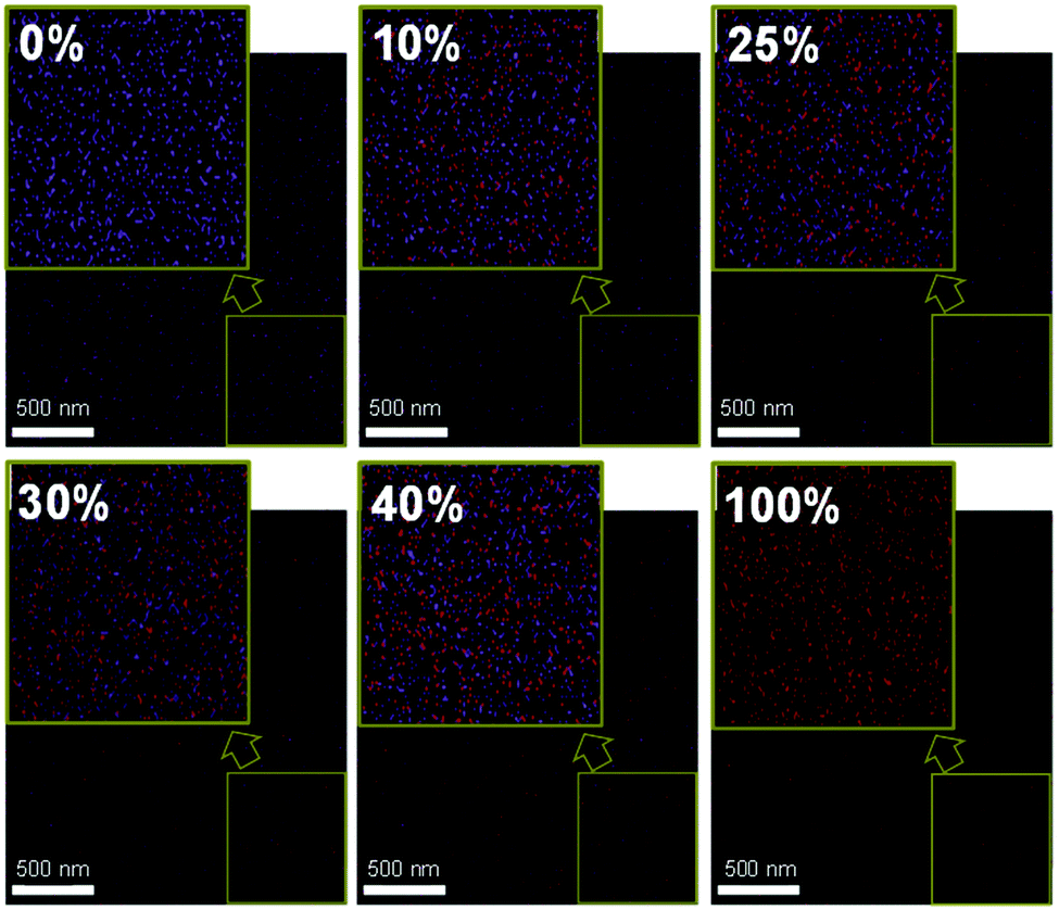 | ||
| Fig. 4 Energy dispersive X-ray elemental mapping; fluorine (purple dots) and nitrogen (red dots) indicate PTB7-Th and DR3TSBDT, respectively, and the inset is the corresponding zoomed images. | ||
External quantum efficiency (EQE) spectra revealed an excellent photocurrent response over the absorption range of 300–800 nm (Fig. 3b). For all devices, the shapes of the EQE plots are similar to the corresponding absorption spectra, indicating that the absorption over the entire wavelength range contributes to photocurrent generation.
Carrier transport and recombination dynamics
To understand the working mechanism and different photovoltaic performances in the tested OSCs, we characterized the charge transport properties and recombination dynamics. The charge carrier mobilities of the hole- and electron-only devices were estimated using a space-charge limited curve (SCLC),47,48 as detailed in the Methods section (Table 1 and ESI,† Fig. S10). With the electron mobilities being relatively constant for all ternary cases, the hole mobilities are sensitive to the DR3TSBDT loading ratios. All blends investigated in this study exhibited highly balanced charge-transport properties (hole/electron mobility ratios of 1.30–1.92). In addition, it was found that both the hole and electron mobilities gradually increased at low DR3TSBDT loadings (0–25 wt%), while a further increase in the DR3TSBDT content caused a decrease in the mobilities. Thus, the ternary OSCs with 25 wt% DR3TSBDT showed a superior mobility level compared to the other samples, implying better percolation pathways for the charge carriers. This is due to the optimized morphology, which is discussed in detail in the following section.We then analyzed the dependence of the J–V characteristics of the devices on light intensity, in order to elucidate the recombination dynamics that can affect the performance. It is well known that a correlation between JSC and illumination intensity (I) exists and follows the relation JSC ∝ Iα (Power law), where α is the unity when all the carriers are swept out prior to the bimolecular recombination process.49,50 As shown in the ESI,† Fig. S11a, the logarithmic plots of JSCversus I show slopes (α) in the range of 0.95–0.98 for the devices with 0–40 wt% DR3TSBDT, along with a slope of 0.92 for the DR3TSBDT:PC71BM binary system. This suggests that the bimolecular recombination loss is minor for all devices except for DR3TSBDT:PC71BM, which correlates with the unsatisfactory performance of DR3TSBDT:PC71BM, especially the low FF.
The device with 25 wt% DR3TSBDT exhibited the weakest bimolecular recombination with an α value of 0.98, which partially explains the highest JSC value and mobility levels observed. Fig. S11b (ESI†) shows a plot of VOC as a function of the logarithm of light intensity. For all cases, a strong dependence of VOC on light intensity with a slope larger than 2kT/q is observed, where k is Boltzmann's constant, T is temperature, and q is elementary charge, suggesting the presence of a trap-assisted recombination.
Film morphology and microstructure
The morphology and microstructure of the blend films were characterized using atomic force microscopy (AFM), high-resolution transmission electron microscopy (HR-TEM), and grazing incidence wide-angle X-ray scattering (GIWAXS). The PTB7-Th:PC71BM host blend film possessed a small-length scale morphology with a root-mean-square (RMS, Rq) roughness of 1.24 nm (Fig. 5a and ESI,† Fig. S12). Incorporating up to 30 wt% DR3TSBDT into the host matrix led to a gradual increase in the uniform features with a nanoscale phase separation. However, a further increase in DR3TSBDT caused a higher roughness with large aggregated regions. In the HR-TEM images of ternary films containing 25ߝ40 wt% DR3TSBDT showed finely dispersed fibrils with domain sizes ranging from 10 to 15 nm, plausibly reflecting an interpenetrating network (Fig. 5b). However, such features were not observed in other films.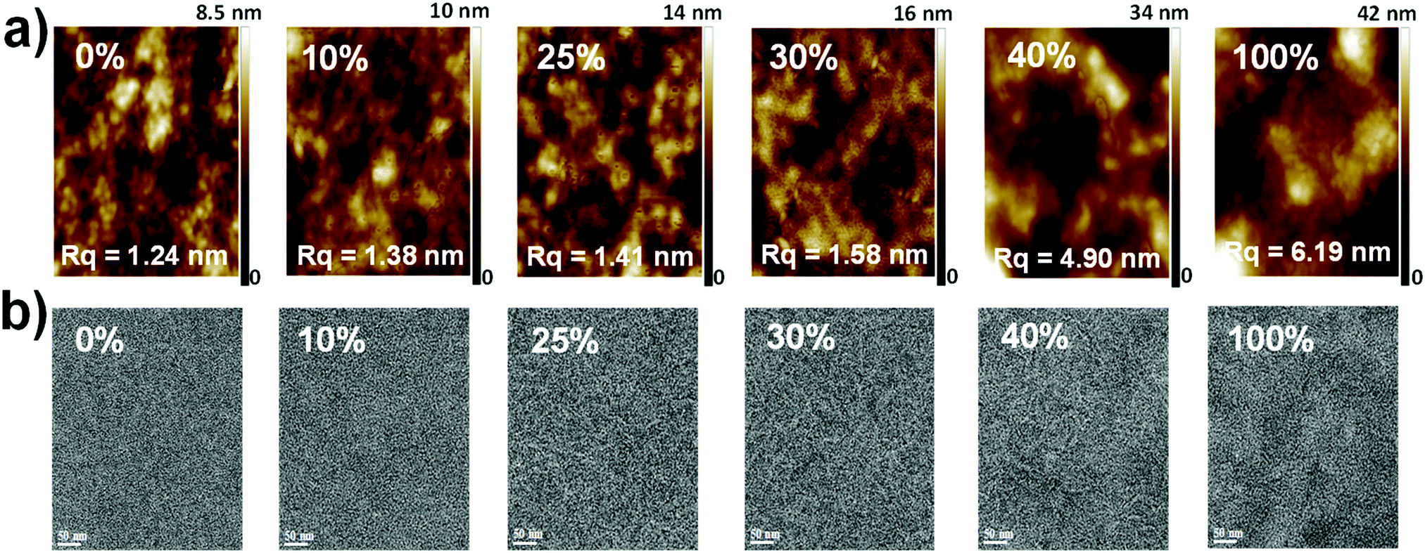 | ||
| Fig. 5 (a) AFM topography images (scan size 1 × 1 μm). (b) HR-TEM images (scale bar 50 nm) of blend films with different DR3TSBDT loading ratios. Different color bars are used for height (AFM) variance. | ||
As seen from the GIWAXS patterns in Fig. 6 and in the ESI,† Fig. S13, PTB7-Th:PC71BM produced a (010) π–π stacking peak centered at about 1.67 Å−1 in the out-of-plane direction (qz) with an arc-like lamellar (100) peak along the in-plane direction (qxy). This indicates a favoured face-on orientation relative to the substrate (see the ESI,† Table S1 for detailed crystallographic parameters). In contrast, in the case of DR3TSBDT:PC71BM, another binary system, the (010) π–π stacking peak was located along the qxy direction in conjunction with the highly ordered lamellar (100), (200), and (300) peaks in the qz axis, suggesting a preferential edge-on alignment. Interestingly, adding DR3TSBDT to form the ternary films resulted in the formation of (010) π–π stacking peaks in both the qxy and qz profiles, providing conclusive evidence for the formation of mixed edge-on and face-on orientations, the so-called 3-D textured structures. In particular, we found that the intensities of both the out-of-plane and in-plane (010) peaks were strengthened for the ternary film in the case of the 25% DR3TSBDT blend (Fig. 7a), which is largely responsible for the enhanced charge transport. Additionally, for all samples the (010) coherence lengths (LCs), which are a measure of cumulative lattice distortions in both the qxy and qz axes, were also calculated using the Scherrer equation51 (Fig. 7b). With the LC values along the qz being relatively consistent for all the cases (4–7 nm), the LC values along the qxy increased from ∼6 to 20 nm with an increase in the DR3TSBDT loading ratios, illustrating that the ternary systems could form larger nanocrystallites than the PTB7-Th:PC71BM host. These changes in the molecular stacking and crystallinity, following the addition of a guest molecule to the host matrix, provide additional evidence for the alloy model proposed in this study.1,3,41,43,52 Another observation that needs to be emphasized is that, compared to the PTB7-Th:PC71BM host system, which has a predominantly face-on orientation, our data for the optimized ternary systems with 3-D textures indicate far better PCEs. This observation reported for the first time, challenges the traditional assumption that a face-on orientation is more favourable for photovoltaic devices because of its vertical charge transportation channel.
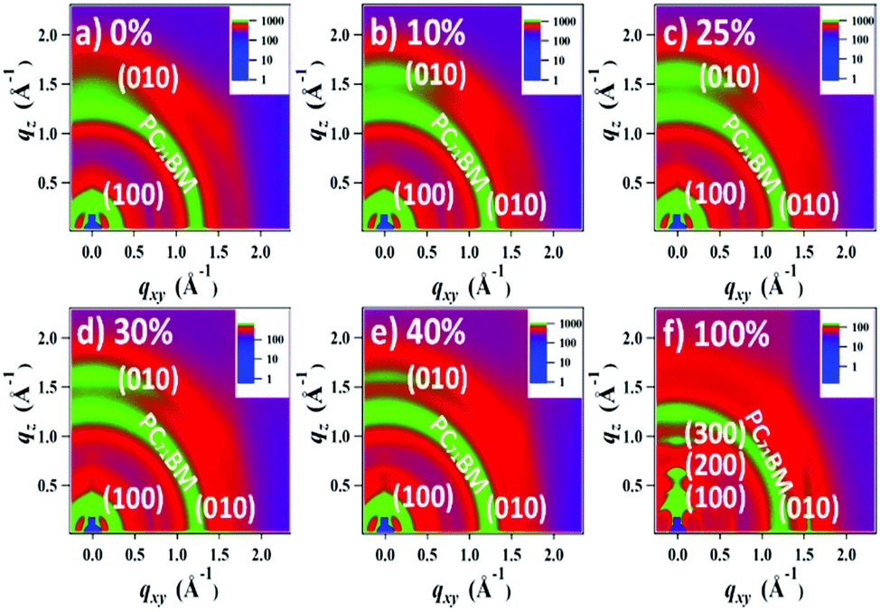 | ||
| Fig. 6 Grazing incidence wide angle X-ray scattering (GIWAXS) patterns of blend films with different DR3TSBDT loading ratios. Different color bars are used for intensity variance. | ||
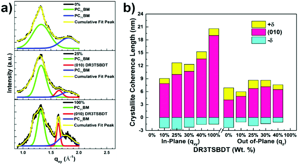 | ||
| Fig. 7 (a) Exemplary fittings of the GIWAXS line cuts at the higher q region in the horizontal direction for PTB7-Th:PC71BM, PTB7-Th–DR3TSBDT (25%):PC71BM and DR3TSBDT:PC71BM blend films. (b) In-plane crystallite coherence length (CCL) of π–π stacking. Gaussian fits were used to determine the peak position and FWHM. | ||
Conclusions
A ternary system comprising DR3TSBDT:PTB7-Th as a donor and PC71BM as an acceptor was investigated in detail, considering both cascaded energy levels and molecular compatibility. At low DR3TSBDT loadings (≤25 wt%) into the host system, synergistic effects such as increased JSC and FF values were observed, which is attributed to enhanced light absorption and charge transport, reduced recombination, and optimized morphology. A notable PCE as high as 12.1% was obtained from ternary OSCs with 25 wt% DR3TSBDT, which is among the highest value reported so far. The intimate mixing properties of two donors enable the formation of an alloy-like model in the present ternary systems, as verified by not only elemental mapping and optical microscopy but also the VOC values and molecular packing/crystallinity. Moreover, we discovered that a mixed face-on and edge-on orientation in ternary OSCs, rather than an almost entirely face-on orientation, yields better photovoltaic performances, which challenges the fundamental idea successfully used in the past to describe high-performance OSCs. This finding provides further impetus for continued research in the field of ternary OSCs in order to understand the interesting and sometimes surprising behaviour of the multiple blending systems.Experimental section
Materials
PTB7-Th was purchased from 1-Material and PC71BM from Ossila. All other commercial reagents, including the solvents used in this study, were purchased from Aldrich Co., Alfa Aesar, and TCI Co. and used without further purification. DR3TSBDT was synthesized as described previously.13 All active materials used in this study were sourced from the same batch, in order to ensure a fair comparison between the experimental and control devices.Device fabrication and characterization
A conventional device was used to assess the performance of the PTB7-Th:PC71BM host system and PTB7-Th:PC71BM-based ternary OSCs by varying the amounts of DR3TSBDT and a total of 108 samples were measured. For device fabrication, ITO-coated glass substrates (12 Ω □−1) were sequentially cleaned via ultrasonication in liquid detergent, de-ionized water, acetone, and isopropanol for 15 min each, and dried in an oven at 70 °C overnight. A thin layer of PEDOT:PSS (Baytron® PVP AI 4083 – H.C. Starck, filtered using a 0.45 μm PVDF syringe filter) was first spin coated on the pre-cleaned and UV-Ozone-treated ITO-coated glass substrates at 4000 rpm. After subsequent annealing at 140 °C for 20 min in an ambient atmosphere, the substrates were immediately transferred to a nitrogen-filled glove box. The active layer was then spin coated to yield a ∼140–150 nm thick film (see the ESI,† Fig. S14). The films were dried in a vacuum for 30 min and a 100 nm-thick Al cathode was thereafter thermally evaporated on top of the organic layer using a mask (device area: 0.13 cm2) under a pressure of <9 × 10⁻⁷ Torr. For the preparation of the active layer solution, 14 mg of donor (PTB7-Th or DR3TSBDT) and 21 mg of PC71BM (1:1.5 ratio) were dissolved in 1 ml of chlorobenzene. The solutions were heated overnight at 60 °C under minimal stirring. Later, 3.0 vol% of DIO was added to the solutions and stirred well for homogeneity. For ternary blending, the two solutions were mixed according to the different weight ratios of the two donors and heated at 60 °C for 1 h under minimal stirring in the glove box.
After fabrication, the J–V measurements for the photovoltaic devices were performed under simulated sunlight (AM 1.5G) at an intensity of 100 mW cm−2 using a Keithley 2365A source measurement unit. The measurements were performed in a nitrogen-filled glove box. Prior to device measurement, the irradiance was calibrated using a standard silicon photodiode. For the certified PCE data, it should be noted that the current, power and device area is the sum of 4 devices (each of 0.075 cm2). The measurement of all four devices in a single time was done according to the rule of the calibration laboratory in order to minimize any overestimation of the PCE. The measurement of 4 devices at a single time resulted in a dramatic loss in the fill factor as the total device area was increased which subsequently increased the number of recombination centers. EQE measurements were performed under an ambient atmosphere by using a QEX7 quantum efficiency measurement system (PV Measurements, Inc.). In addition, the deviations between the integral current densities and the JSC values from the J–V measurements were found to be below 10%. For mobility measurements, the hole- and electron-only devices were fabricated using a device architecture of ITO/PEDOT:PSS/active layer/Au and ITO/Al/active layer/Al, respectively. The hole (μh) and electron (μe) mobilities were measured using the SCLC method, which is described by the Mott–Gurney square law as
| JSCLC = (9/8)ε0εTμ((V2)/(L3)) |
Measurements
Thin films for all characterization methods were prepared using the same processing conditions as used for device fabrication and were characterized under an ambient atmosphere. For the absorption, PL emission, optical microscopy, and thickness measurements of the ternary films, the samples were fabricated on a glass substrate. For all other characterization methods, the samples were fabricated on a silicon substrate. UV-vis spectra were obtained using a UV-1800 (SHIMADZU) spectrophotometer and the absorption coefficient was obtained using the following equation:| α = 2.303 × (A/l) |
Acknowledgements
C. Y. conceptualized the project. T. K. carried out the experiments and performed the device fabrication, as well as analyzed the data. S. M. L. synthesized DR3TSBDT. T. K. and C. Y. wrote the manuscript. This work was supported by the National Research Foundation of Korea (NRF) grant funded by the Korea government (MSIP) (2015R1A2A1A10053397). GIWAXD measurements at PLS-II 6D UNIST-PAL beamline and 9A beamline were supported in part by MEST, POSTECH, and UNIST UCRF.Notes and references
- Q. An, F. Zhang, J. Zhang, W. Tang, Z. Deng and B. Hu, Energy Environ. Sci., 2016, 9, 281–322 Search PubMed.
- J. Subbiah, B. Purushothaman, M. Chen, T. Qin, M. Gao, D. Vak, F. H. Scholes, X. Chen, S. E. Watkins, G. J. Wilson, A. B. Holmes, W. W. H. Wong and D. J. Jones, Adv. Mater., 2015, 27, 702–705 CrossRef CAS PubMed.
- J. Zhang, Y. Zhang, J. Fang, K. Lu, Z. Wang, W. Ma and Z. Wei, J. Am. Chem. Soc., 2015, 137, 8176–8183 CrossRef CAS PubMed.
- S. Zhang, L. Ye and J. Hou, Adv. Energy Mater., 2016, 60, 1502529 CrossRef.
- M. C. Scharber, D. Mühlbacher, M. Koppe, P. Denk, C. Waldauf, A. J. Heeger and C. J. Brabec, Adv. Mater., 2006, 18, 789–794 CrossRef CAS.
- J. D. Servaites, B. M. Savoie, J. B. Brink, T. J. Marks and M. A. Ratner, Energy Environ. Sci., 2012, 5, 8343–8350 CAS.
- W. Chen, Z. Du, M. Xiao, J. Zhang, C. Yang, L. Han, X. Bao and R. Yang, ACS Appl. Mater. Interfaces, 2015, 7, 23190–23196 CAS.
- S. Guo, J. Ning, V. Körstgens, Y. Yao, E. M. Herzig, S. V. Roth and P. Müller-Buschbaum, Adv. Energy Mater., 2015, 5, 1401315 CrossRef.
- Y. Liu, J. Zhao, Z. Li, C. Mu, W. Ma, H. Hu, K. Jiang, H. Lin, H. Ade and H. Yan, Nat. Commun., 2014, 5, 5293 CrossRef CAS PubMed.
- F. C. Krebs, Sol. Energy Mater. Sol. Cells, 2009, 93, 394–412 CrossRef CAS.
- J. M. Lee, J. Lim, N. Lee, H. I. Park, K. E. Lee, T. Jeon, S. A. Nam, J. Kim, J. Shin and S. O. Kim, Adv. Mater., 2015, 27, 1519–1525 CrossRef CAS PubMed.
- W. Shockley and H. J. Queisser, J. Appl. Phys., 1961, 32, 510–519 CrossRef CAS.
- B. Kan, Q. Zhang, M. Li, X. Wan, W. Ni, G. Long, Y. Wang, X. Yang, H. Feng and Y. Chen, J. Am. Chem. Soc., 2014, 136, 15529–15532 CrossRef CAS PubMed.
- S. Liu, P. You, J. Li, J. Li, C.-S. Lee, B. S. Ong, C. Surya and F. Yan, Energy Environ. Sci., 2015, 8, 1463–1470 CAS.
- Y. Liu, J. Zhao, Z. Li, C. Mu, W. Ma, H. Hu, K. Jiang, H. Lin, H. Ade and H. Yan, Nat. Commun., 2014, 5, 5293 CrossRef CAS PubMed.
- J. Zhao, Y. Li, G. Yang, K. Jiang, H. Lin, H. Ade, W. Ma and H. Yan, Nat. Energy, 2016, 1, 15027 CrossRef.
- T. Ameri, G. Dennler, C. Lungenschmied and C. J. Brabec, Energy Environ. Sci., 2009, 2, 347–363 CAS.
- J. Gilot, M. M. Wienk and R. A. J. Janssen, Appl. Phys. Lett., 2007, 90, 143512 CrossRef.
- J. D. Kotlarski and P. W. M. Blom, Appl. Phys. Lett., 2011, 98, 053301 CrossRef.
- J. You, L. Dou, K. Yoshimura, T. Kato, K. Ohya, T. Moriarty, K. Emery, C.-C. Chen, J. Gao, G. Li and Y. Yang, Nat. Commun., 2013, 4, 1446 CrossRef PubMed.
- J. Yang, R. Zhu, Z. Hong, Y. He, A. Kumar, Y. Li and Y. Yang, Adv. Mater., 2011, 23, 3465–3470 CrossRef CAS PubMed.
- H. Cha, D. S. Chung, S. Y. Bae, M.-J. Lee, T. K. An, J. Hwang, K. H. Kim, Y.-H. Kim, D. H. Choi and C. E. Park, Adv. Funct. Mater., 2013, 23, 1556–1565 CrossRef CAS.
- S. Honda, H. Ohkita, H. Benten and S. Ito, Chem. Commun., 2010, 46, 6596–6598 RSC.
- M. Koppe, H.-J. Egelhaaf, G. Dennler, M. C. Scharber, C. J. Brabec, P. Schilinsky and C. N. Hoth, Adv. Funct. Mater., 2010, 20, 338–346 CrossRef CAS.
- L. Lu, W. Chen, T. Xu and L. Yu, Nat. Commun., 2015, 6, 7327 CrossRef CAS PubMed.
- Q. An, F. Zhang, L. Li, J. Wang, J. Zhang, L. Zhou and W. Tang, ACS Appl. Mater. Interfaces, 2014, 6, 6537–6544 CAS.
- Q. An, F. Zhang, Q. Sun, J. Wang, L. Li, J. Zhang, W. Tang and Z. Deng, J. Mater. Chem. A, 2015, 3, 16653–16662 CAS.
- M. E. Farahat, D. Patra, C.-H. Lee and C.-W. Chu, ACS Appl. Mater. Interfaces, 2015, 7, 22542–22550 CAS.
- J.-H. Huang, M. Velusamy, K.-C. Ho, J.-T. Lin and C.-W. Chu, J. Mater. Chem., 2010, 20, 2820–2825 RSC.
- T.-Y. Huang, D. Patra, Y.-S. Hsiao, S. H. Chang, C.-G. Wu, K.-C. Ho and C.-W. Chu, J. Mater. Chem. A, 2015, 3, 10512–10518 CAS.
- P. P. Khlyabich, B. Burkhart and B. C. Thompson, J. Am. Chem. Soc., 2011, 133, 14534–14537 CrossRef CAS PubMed.
- L. Yang, H. Zhou, S. C. Price and W. You, J. Am. Chem. Soc., 2012, 134, 5432–5435 CrossRef CAS PubMed.
- L. Lu, M. A. Kelly, W. You and L. Yu, Nat. Photonics, 2015, 9, 491–500 CrossRef CAS.
- B. M. Savoie, S. Dunaisky, T. J. Marks and M. A. Ratner, Adv. Energy Mater., 2015, 5, 1400891 CrossRef.
- H. Lu, X. Zhang, C. Li, H. Wei, Q. Liu, W. Li and Z. Bo, Macromol. Rapid Commun., 2015, 36, 1348–1353 CrossRef CAS PubMed.
- L. Lu, T. Xu, W. Chen, E. S. Landry and L. Yu, Nat. Photonics, 2014, 8, 716–722 CrossRef CAS.
- B. C. Thompson, Y.-G. Kim and J. R. Reynolds, Macromolecules, 2005, 38, 5359–5362 CrossRef CAS.
- L. Xiao, K. Gao, Y. Zhang, X. Chen, L. Hou, Y. Cao and X. Peng, J. Mater. Chem. A, 2016, 4, 5288–5293 CAS.
- S. Zhang, L. Zuo, J. Chen, Z. Zhang, J. Mai, T.-K. Lau, X. Lu, M. Shi and H. Chen, J. Mater. Chem. A, 2016, 4, 1702–1707 CAS.
- N. Gasparini, X. Jiao, T. Heumueller, D. Baran, G. J. Matt, S. Fladischer, E. Spiecker, H. Ade, C. J. Brabec and T. Ameri, Nat. Energy, 2016, 1, 16118 CrossRef.
- L. Yang, L. Yan and W. You, J. Phys. Chem. Lett., 2013, 4, 1802–1810 CrossRef CAS PubMed.
- Z. He, B. Xiao, F. Liu, H. Wu, Y. Yang, S. Xiao, C. Wang, T. P. Russell and Y. Cao, Nat. Photonics, 2015, 9, 174–179 CrossRef CAS.
- D. Angmo, M. Bjerring, N. C. Nielsen, B. C. Thompson and F. C. Krebs, J. Mater. Chem. C, 2015, 3, 5541–5548 RSC.
- S. Holliday, R. S. Ashraf, A. Wadsworth, D. Baran, S. A. Yousaf, C. B. Nielsen, C.-H. Tan, S. D. Dimitrov, Z. Shang, N. Gasparini, M. Alamoudi, F. Laquai, C. J. Brabec, A. Salleo, J. R. Durrant and I. McCulloch, Nat. Commun., 2016, 7, 11585 CrossRef CAS PubMed.
- N. Li, F. Machui, D. Waller, M. Koppe and C. J. Brabec, Sol. Energy Mater. Sol. Cells, 2011, 95, 3465–3471 CrossRef CAS.
- C. M. S. Vicente, P. S. André and R. A. S. Ferreira, Rev. Bras. Ensino Fis., 2012, 34, 1–5 CrossRef.
- C. Goh, R. J. Kline, M. D. McGehee, E. N. Kadnikova and J. M. J. Fréchet, Appl. Phys. Lett., 2005, 86, 122110 CrossRef.
- G. G. Malliaras, J. R. Salem, P. J. Brock and C. Scott, Phys. Rev. B: Condens. Matter Mater. Phys., 1998, 58, R13411 CrossRef CAS.
- I. Riedel, J. Parisi, V. Dyakonov, L. Lutsen, D. Vanderzande and J. C. Hummelen, Adv. Funct. Mater., 2004, 14, 38–44 CrossRef CAS.
- P. Schilinsky, C. Waldauf and C. J. Brabec, Appl. Phys. Lett., 2002, 81, 3885–3887 CrossRef CAS.
- T. Kumari, M. Moon, S.-H. Kang and C. Yang, Nano Energy, 2016, 24, 56–62 CrossRef CAS.
- T. Ameri, P. Khoram, J. Min and C. J. Brabec, Adv. Mater., 2013, 25, 4245–4266 CrossRef CAS PubMed.
Footnotes |
| † Electronic supplementary information (ESI) available: Additional figures (UV vis, J–V characteristics, surface energy measurement, EDAX, optical microscopy, AFM phase images, charge transport characteristics (SCLC), GIWAXS analyses and thickness measurement of the ternary OPVs) and table (crystallographic parameters of the ternary OPV thin films). See DOI: 10.1039/c6ee02851a |
| ‡ T. K. and S. M. L. contributed equally to this work. |
| This journal is © The Royal Society of Chemistry 2017 |