
Highly crystalline low-bandgap polymer nanowires towards high-performance thick-film organic solar cells exceeding 10% power conversion efficiency†
Jaewon
Lee‡
,
Dong Hun
Sin‡
,
Byungho
Moon
,
Jisoo
Shin
,
Heung Gyu
Kim
,
Min
Kim
and
Kilwon
Cho
*
Department of Chemical Engineering, Pohang University of Science and Technology, Pohang, 790–784, Korea. E-mail: kwcho@postech.ac.kr
First published on 22nd November 2016
Abstract
Preparing polymer nanowire (PNW) structures using donor–acceptor (D–A) conjugated polymers is one promising strategy to improve the power conversion efficiencies (PCEs) of bulk-heterojunction (BHJ) polymer solar cells (PSCs). Here, we report that a high PCE of 10.62% was obtained with a single-junction inverted cell with a 350 nm thick active layer containing highly crystalline PNWs based on a D–A conjugated polymer (P4TNTz-2F), which possesses a deep-lying HOMO level (−5.46 eV) and a low-bandgap (1.59 eV) as well as a planar/rigid backbone. The thick active layer in the P4TNTz-2F![[thin space (1/6-em)]](https://www.rsc.org/images/entities/char_2009.gif) :PC71BM-based PSC absorbs incident light almost completely, which in turn contributes to a high short-circuit current density of 19.45 mA cm−2. This high PCE is attributed to the continuous and evenly distributed polymer network with narrow PNWs (≈6 nm in width and several hundred nanometers in length) in the thick film blended with PC71BM, which facilitates charge separation (QPL ≈ 98%) and transport (μh = 8.31 × 10⁻³ cm2 V−1 s−1). Moreover, this PNW structure in the BHJ active layer can be prepared using a facile film-forming process at a mild blending temperature (≈70 °C), which means that high efficiency BHJ PSCs can be fabricated with good reproducibility. These results demonstrate the great promise of polymer nanowire solar cells and provide important scientific insights that facilitate further improvements in the morphologies and performances of organic solar cells through material design and development.
:PC71BM-based PSC absorbs incident light almost completely, which in turn contributes to a high short-circuit current density of 19.45 mA cm−2. This high PCE is attributed to the continuous and evenly distributed polymer network with narrow PNWs (≈6 nm in width and several hundred nanometers in length) in the thick film blended with PC71BM, which facilitates charge separation (QPL ≈ 98%) and transport (μh = 8.31 × 10⁻³ cm2 V−1 s−1). Moreover, this PNW structure in the BHJ active layer can be prepared using a facile film-forming process at a mild blending temperature (≈70 °C), which means that high efficiency BHJ PSCs can be fabricated with good reproducibility. These results demonstrate the great promise of polymer nanowire solar cells and provide important scientific insights that facilitate further improvements in the morphologies and performances of organic solar cells through material design and development.
Broader contextThe development of new semi-conducting polymers plays a critical role in improving the power conversion efficiencies (PCE) of bulk-heterojunction (BHJ) polymer solar cells (PSCs). As a result of the many attempts to design high performance photovoltaic polymers, the PCEs of PSCs have improved tremendously over the past few decades. However, thick active layers generally provide low PCEs, which is probably due to the inferior charge carrier mobilities of semi-conducting polymers and is still a hurdle for the commercial applications of PSCs to overcome. Among the various approaches for the fabrication of high performance PSCs with thick active layers, the preparation of donor–acceptor (D–A) conjugated polymer nanowires is one promising strategy for constructing a near-optimum BHJ morphology without degrading the fill factor. In this paper, we report a D–A conjugated polymer that is the product of a clear molecular design strategy for polymer nanowire formation, and a 350 nm thick single-junction inverted cell with a high PCE of 10.62%. We believe that our findings establish a bright future for the large-scale commercialization of organic solar technologies. |
Introduction
Polymer solar cells (PSCs) with a bulk-heterojunction (BHJ) structure have been regarded as next-generation solar cells due to their advantages of low cost, light weight, solution processability, mechanical flexibility, and rapid energy payback time.1–4 To date, single-junction BHJ PSCs with PCEs up to 10% have been realized.5–7 However, most reported BHJ systems achieve optimal performances with active layer films close to 100 nm in thickness, but it is very difficult to reproducibly fabricate uniform and defect-free films with such thickness over large areas at high printing rates, as required in the future commercialization of organic solar technologies.8 The increased bimolecular charge recombination of photogenerated charge carriers and the space charge effects induced by the low charge carrier mobilities of BHJ components decrease the fill factor (FF) and the PCE, which precludes the use of thick active layers for most BHJ materials.9 Additionally, thin films (≈100 nm) comprised of reported BHJ materials do not completely absorb incident light, whereas the use of films with thicknesses in the order of 250–300 nm enables nearly total utilization of incident above-bandgap light.10,11 Therefore, there remains a significant need to design novel semi-conducting polymers with high charge carrier mobilities, as well as to develop BHJ morphologies with a bicontinuous interpenetrating network of donor and acceptor crystalline nanostructures so as to achieve highly efficient PSCs with thick active layers.One of the most promising approaches to the construction of near-optimum BHJ morphologies in thick active layers involves the incorporation of self-assembled polymer nanostructures.8,9,12,13 Of the numerous nanostructures based on conjugated polymers including nanoplates, nanowires, nanofibers, and nanoribbons, one-dimensional (1D) polymer nanowires (PNWs) with long-range π-connectivity14–17 and appropriate width (<10 nm) are ideal for use in BHJ PSCs because of their superior carrier transport and the increased interfacial area between the donor and the acceptor.18 There have been several reports of solution-processed PNW solar cells based on regioregular poly(3-alkylthiophene) (RR-P3AT) with improved PCEs.12,13,19,20 An interconnected network of self-assembled P3AT domains provides continuous percolation pathways for charge carriers, which means that the optimum thickness is increased and a higher current is produced. Despite the well-defined self-assembled PNW formation possible with P3AT, the intrinsic properties of P3AT have several limitations, such as limited light harvesting breadth, frontier orbital levels, and a low charge carrier mobility.
D–A alternating copolymers with electron-donating (D) and electron-accepting (A) units in a conjugated backbone have recently been identified as the most successful materials for BHJ PSCs because of their tunable band gaps and energy levels, and their superior charge carrier mobility due to the intramolecular charge transfer (ICT) between their D- and A-units.21,22 We recently developed a PNW solar cell based on a D–A conjugated polymer (PBDT2FBT-2EHO) that exhibits outstanding improvement in PCE from 5.19 to 8.2% and an increase in hole mobility by a factor of 70 when compared to those of devices without PNWs.23 These results suggest that the preparation of PNW solar cells with D–A conjugated polymers is a promising route to fabricate state-of-the-art PSCs. However, it is difficult to grow crystalline nanowire structures consisting of D–A conjugated polymers with long polymer chains, chain disorder, and bulky solubilizing groups,16 particularly when they are blended with fullerene derivatives. Consequently, only a few 1D nanowires with desirable dimensions have been successfully constructed in BHJ PSCs with D–A conjugated polymers.23,24 There remain significant challenges to the development of highly soluble and crystalline D–A conjugated polymers that permit crystalline 1D PNW formation and facile solution-processable thick film fabrication.
Here, we report highly efficient PNW BHJ solar cells with the best PCE of 10.62% and a BHJ active layer with a very thick optimum thickness (≈350 nm), which were achieved through the introduction of a semi-crystalline D–A conjugated polymer (P4TNTz-2F, Fig. 1a) and BHJ morphology engineering. P4TNTz-2F was designed to consist of naphtho[1,2-c:5,6-c′]bis[1,2,5]thiadiazole (NTz) and 3,3-dibromo-2,2-bithiophene (2F2T) units in order to ensure a rigid backbone conformation for the formation of 1D PNW structures. PNW structures can be successfully prepared in BHJ active layers by performing a facile film-forming process at a mild blending temperature (≈70 °C), which provides high efficiency BHJ PSCs with good reproducibility. We found that the 1D PNW structures of P4TNTz-2F have appropriate dimensions (6 ± 1 nm in width and a few hundred nanometers in length) and a well-distributed spatial density within the thick films, which results in a large donor/acceptor interfacial area and a high charge carrier mobility. The best performance of the resulting PNW solar cells based on a blend of P4TNTz-2F and [6,6]-phenyl-C71butyric acid methyl ester (PC71BM) was a high short-circuit current density (JSC) of 19.45 mA cm−2, an open-circuit voltage (VOC) of 0.82 V, a fill factor (FF) of 66.5%, and a PCE of 10.62%.
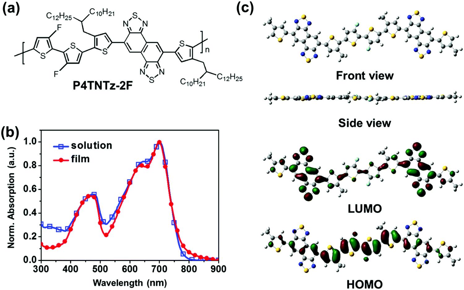 | ||
| Fig. 1 (a) Molecular structure of P4TNTz-2F. (b) UV-vis absorption spectra of P4TNTz-2F (M-MW) in CB solution and as a thin film. (c) Minimum energy conformations and frontier molecular orbitals of the P4TNTz-2F model molecule with methyl-trimmed alkyl chains using DFT calculations (B3LYP/6-31G*). | ||
Results and discussion
Fluorination of heterocycles in D–A conjugated polymers induces deep-lying highest occupied molecular orbital (HOMO) levels and promotes backbone planarization via nonbonding interactions that produce a higher VOC and improved charge carrier mobility, respectively.5,6,25 However, in some cases, D–A conjugated polymers based on fluorinated heterocycles have been reported to exhibit overly segregated BHJ morphologies;5,6,23,26 such a tendency necessitates harsh film preparation conditions such as a high blending temperature or preheating of the substrate (>100 °C) in order to ensure near-optimum BHJ morphologies. Therefore, the degree of fluorination in one repeating unit of the polymer must be optimized in order to achieve highly efficient PSCs.27NTz is a tetracyclic heteroaromatic compound, in which two 2,1,3-benzothiadiazole (BT) rings are fused. Compared with BT, NTz has an enlarged planar aromatic structure and strong electron deficiency, which result in highly crystalline structures and efficient solar energy harvesting of NTz-based D–A conjugated polymers; this leads to high charge carrier mobilities and device performances in organic field effect transistors (OFETs) and PSCs.5,7,28–31 Despite their promising optoelectronic properties, only a few NTz-based D–A conjugated polymers for use in solution-processed bulk-heterojunction solar cells have been reported.
With these considerations in mind, we designed a D–A conjugated polymer (P4TNTz-2F, Fig. 1a) to combine the advantages of the fluorinated heterocyclic unit (3,3-difluoro-2,2-bithiophene, 2F2T) and the NTz unit and thereby prepare 1D polymer nanowires of P4TNTz-2F in a BHJ active layer. Computational calculations were performed using the density functional theory (DFT, B3LYP/6-31G* level)32 to investigate the backbone conformation and frontier molecular orbitals of this polymer. The control molecule comprising of 5,6-difluoro-2,1,3-benzothiadiazole (2FBT) and 2F2T units27 was also calculated for comparison. Fig. S1 (ESI†) shows the torsional profiles of the constitutive building blocks 1T-NTz and 1T-2FBT. The linkage between thiophene and NTz (or 2FBT) prefers a planar conformation (dihedral angle: ∼180°), possibly because of the intramolecular hydrogen bonding between the hydrogen in thiophene and the nitrogen in NTz (or 2FBT).28 According to the torsional profiles of 1T-NTz and 1T-2FBT, there are two minimum energy conformations for the thiophene–NTz and thiophene–2FBT linkages. These minimum energy conformations are expected to repeat randomly in the polymeric backbone;25 three representative possible conformations (PC) of the conjugated backbone have been identified (Fig. S2, ESI†).23,33 However, it is reasonable to assume a trans conformation of the two alkylated thiophenes that sandwich NTz, in which the sulfur atoms in the thiophene rings point in the opposite direction to the NTz core so as to minimize the steric impact between the hydrogen atoms on the thiophene rings and the NTz core.28 In addition, NTz has a centrosymmetric structure that favors the trans arrangement of the flanking thiophenes, whereas 2FBT has an axisymmetric structure (Fig. S3, ESI†).28 Therefore, NTz-based polymers are likely to have a more regular arrangement of heterocyclics and side chains than 2FBT-based polymers (Fig. S3, ESI†), which is beneficial for polymer packing and charge transport.
Our DFT calculations predict that the use of the 2F2T unit as a fluorinated heterocyclic building block will enhance backbone planarity and decrease the HOMO level of the NTz-based polymer (Fig. 1c, Fig. S4, and Table S1, ESI†). Note that the backbone planarity of the P4TNTz-2F model compound is comparable to that of the P4T2FBT-2F model compound, which has four fluorine substituents (4F) in its repeating unit. P4TNTz-2F with the appropriate degree of fluorination (2F) would provide a favorable nanoscale BHJ morphology when blended with fullerenes.27 The molecular orbital distributions are well delocalized in the P4TNTz-2F model molecule, which indicates that intramolecular charge transfer between the D and A units will be efficient. The HOMO/lowest unoccupied molecular orbital (LUMO) levels of the P4TNTz-2F model compound (2F) are downshifted by ≈0.4 eV with respect to those of the P4TNTz model compound (0F), and their bandgaps are nearly identical.
Motivated by the encouraging results of the DFT calculations, the P4TNTz-2F polymer based on 2F2T and NTz units was synthesized. The detailed synthetic procedures for the monomers and polymers are described in the ESI.† To ensure polymer solubility and thus ease of processing for the fabrication of solar cells, it is important to attach branched alkyl chains at the beta positions of the thiophene rings.5 With regards to the size of the branched alkyl chains, the common choices include 2OD (2-octyldodecyl) and 2DT (2-decyltetradecyl) for the combination of the tetrathiophene and BT (or NTz)-based conjugated backbone.6 However, the P4TNTz-2F-OD polymer with a 2OD alkyl chain (Scheme S5, ESI†) exhibits extremely poor solubility in common chlorinated organic solvents including chloroform (CF), chlorobenzene (CB), and o-dichlorobenzene (DCB) even at elevated temperatures. Therefore, the longer alkyl chain 2DT was incorporated in the P4TNTz-2F polymer to obtain the appropriate solubility for film processing (Scheme S6, ESI†). P4T2FBT-2F was also prepared and used as a control polymer (Scheme S7, ESI†). The reaction time of polymerization was controlled to afford P4TNTz-2F polymers with various molecular weights (24 h, 48 h, and 72 h for low-molecular weight, medium-molecular weight, and high-molecular weight, respectively). The crude P4TNTz-2F polymers were purified by performing Soxhlet extractions with methanol, acetone, n-hexane, CF, CB, and DCB. The CF, CB, and DCB fractions obtained from 24 h, 48 h, and 72 h reaction times, respectively, were concentrated, and the products were precipitated in methanol to obtain the target conjugated polymers as black solids. The number-average molecular weights (Mn) and the weight-average molecular weight (Mw) were evaluated using high-temperature gel-permeation chromatography (GPC) using 1,2,4-trichlorobenzene as the eluent at 160 °C. The Mn values of the P4TNTz-2F polymers were 11.8, 18.3, and 29.3 kDa with polydispersity indices (PDIs) of 2.24, 1.85, and 2.29 for the CF (low molecular weight; L-MW), CB (medium molecular weight; M-MW), and DCB (high molecular weight; H-MW) fractions, respectively.
P4TNTz-2F exhibits good thermal stability, regardless of the molecular weight, with a decomposition temperature (Td, 5% weight loss) of approximately 430 °C under a nitrogen atmosphere, as measured using thermogravimetric analysis (TGA, Fig. S8, ESI†). No obvious thermal transitions are evident for P4TNTz-2F below 350 °C in the differential scanning calorimetry (DSC, Fig. S9, ESI†) results for the second heating and cooling runs. In contrast, the control polymer P4T2FBT-2F undergoes an endothermic melting transition (Tm = 299 °C) during heating and an exothermic aggregation transition (Tc = 285 °C) during cooling. These results indicate that P4TNTz-2F is more rigid than P4T2FBT-2F,28,31 which is attributed to the enlarged π-heterocyclic and centrosymmetric NTz unit, which favorably adopts the trans arrangement of flanking thiophenes and thus affords a more linear backbone than P4T2FBT-2F.
The UV-vis absorption spectra of P4TNTz-2F in dilute CB solution and as thin films are shown in Fig. 1b and Fig. S10 (ESI†). The absorption maxima (λmax) and the optical band gaps (Eoptg) are summarized in Table S2 (ESI†). The spectra of the CB solutions and thin films of the P4TNTz-2F samples contain three well-defined absorption bands. The intense vibronic peak (A0–0) at ≈699 nm for M-MW in CB is comparable to that at ≈697 nm of the thin film, which indicates that the conjugated backbone of P4TNTz-2F possesses a highly planar structure via non-covalent intramolecular interactions in solution. The long-wavelength absorption bands (A0–1) with well-resolved vibronic peaks (A0–0) in the range 500–900 nm are assigned to intramolecular charge transfer (ICT) transitions from the donor units to the acceptor units in the polymer backbone.34 The NTz-based polymer (P4TNTz-2F) has a smaller bandgap with a red-shift of ≈25 nm with respect to the spectrum of the 2FBT-based polymer (P4T2FBT-2F), which is due to the stronger electron deficiency of the NTz unit.
The intensity ratio for the 0–0 to the 0–1 transition of P4TNTz-2F varies significantly with its molecular weight. It is well known that the higher the magnitude of the vibronic peak (0–0 transition), the more ordered the microstructure.31 Note that both the absorption peak and the onset of the H-MW polymer film are significantly blue-shifted with respect to those of the L-MW polymer film. This blue-shift indicates that the conjugated backbone of the H-MW polymer is not fully planarized during the rapid spin-casting film-formation process; as the H-MW polymer is deposited from a warm solution onto the substrate, the polymer conformation is kinetically quenched before it reaches a sufficient level of planarization due to lower solubility.35 In contrast, the L-MW polymer is more likely to become planarized because its better solubility provides sufficient time to kinetically extend the polymer conformation, leading to an increase of conjugation length and absorption breadth.
Cyclic voltammetry (CV) was then utilized to measure the onset redox potentials of the polymers (Fig. S11, ESI†). The HOMO/LUMO energy levels for P4TNTz-2F are −5.46/−3.55 eV (the energy levels vary only slightly with the molecular weight), which means that the driving force is sufficient for charge separation and electron transfer when blended with fullerene derivatives. Note that the deep-lying HOMO level of the NTz-based polymer (P4TNTz-2F) is comparable to that of the 2FBT-based polymer (P4T2FBT-2F), which contributes to a high VOC in PSCs.36
The crystalline nature and molecular orientations of the P4TNTz-2F polymers with various molecular weights were studied using two-dimensional grazing-incidence X-ray diffraction (2D GIXD) analysis. Fig. 2 and Fig. S12 (ESI†) show the 2D GIXD patterns of the as-spun and thermally annealed (at 230 °C) polymer thin films on Si substrates, and the corresponding 1D diffractogram profiles are summarized in Table S3 (ESI†). In the 2D GIXD patterns of all the polymer thin films, which were as-spun and thermally annealed, the (h00) reflections are dominantly observed along the out-of-plane direction, confirming that the texture of the films adopts edge-on crystallites with respect to the substrates.37 The intense (100) diffraction peaks of P4TNTz-2F at qz = 0.26 Å−1 correspond to an interchain distance of ≈24 Å. Note that the (00l) reflections along the in-plane directions clearly appeared, which results from the rigid conjugated backbones.38 The (002) reflections correspond to a distance of around 10.7 Å, which is approximately half of the repeating unit length (21.8 Å) of P4TNTz-2F (Fig. 2c). When D–A conjugated polymers form a solid, the donor and acceptor units are packed alternately due to the strong intermolecular interactions between the electron-rich (donor) and electron-deficient (acceptor) moieties.39,40 Therefore, these (00l) reflections imply that there is significant order along the backbone direction, which is possibly induced by the regularly repeating trans configuration of the NTz and flanking thiophene units in the coplanar polymer chains. In contrast, the (00l) reflection is not evident along the in-plane direction of the 2D GIXD patterns of the P4T2FBT-2F polymer thin films (Fig. S13, ESI†).
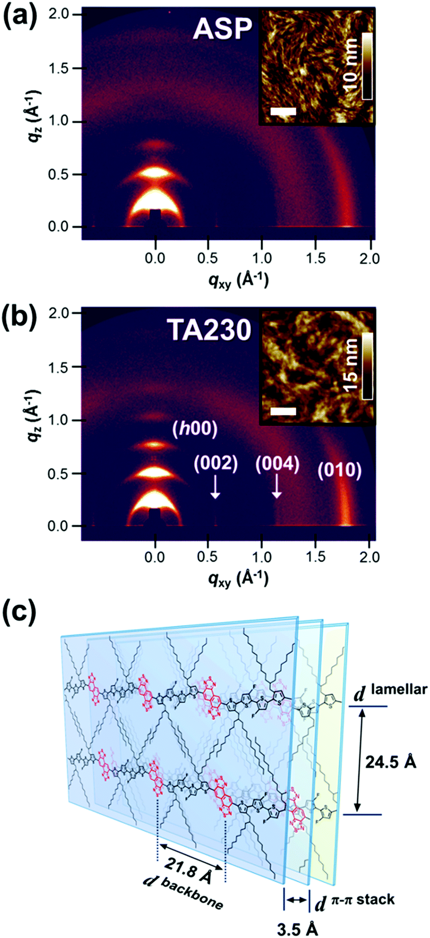 | ||
| Fig. 2 2D GIXD patterns of the P4TNTz-2F (M-MW) polymer as (a) an as-spun thin film and (b) a thermally annealed thin film at 230 °C. The insets are the AFM height images of the corresponding thin films, where the scale bars are 500 nm. (c) Schematic of the molecular packing of P4TNTz-2F based on data from X-ray scattering and DFT calculations. | ||
After thermal annealing, the 2D GIXD patterns contain clear (h00) reflections up to the fifth order along the out-of-plane direction and intense (010) reflections along the in-plane direction, which indicates the superior crystallinity of the P4TNTz-2F polymers. The high crystallinity evident in the 2D GIXD images is consistent with the observed atomic force microscopy (AFM) morphologies (see the insets in Fig. 2). The π–π stacking distances of the P4TNTz-2F samples are similar, approximately 3.5 Å, regardless of their molecular weight. Interestingly, as the Mn increases for the thermally annealed films, the lamellar diffractions tend to appear preferentially on the qz axis and the π–π stacking diffraction converges onto the qxy axis, which indicates a strong tendency to adopt an edge-on orientation (Fig. S12, ESI†).41
Polymer field-effect transistor (PFET) devices were fabricated to investigate the charge carrier transport properties of P4TNTz-2F. These devices have a bottom-gate-top-contact architecture with octadecyltrimethoxysilane (OTS)-treated SiO2 (300 nm)/Si substrates. The PFET performances were optimized by annealing at 230 °C for 30 min, and the P4TNTz-2F polymers were found to exhibit the typical behavior of a p-channel transistor (Fig. S14, ESI†). The hole mobility (μh) of M-MW P4TNTz-2F was evaluated in the saturation regime and found to be as high as 1.07 cm2 V−1 s−1, with a current on/off ratio of ∼107 (Table S4, ESI†). The excellent charge transport properties of P4TNTz-2F are probably due to its highly crystalline features, which result from its planar/rigid backbone and strong push–pull ICT strength. For the thermally annealed films, the M-MW polymer exhibits a higher degree of molecular order than the H-MW polymer, as evident in the stronger intensity of the lamellar (qz, 100) reflection peak (Fig. S12, ESI†) and the large (qz, 100) coherence length (Table S3, ESI†). The μh (FET) values of P4TNTz-2F are 0.52, 1.07, and 0.89 cm2 V−1 s−1 for L-MW, M-MW, and H-MW, respectively; this order is consistent with the crystallinity order.
To characterize the photovoltaic properties of P4TNTz-2F, inverted BHJ PSCs were fabricated. The device structure was ITO/ZnO/P4TNTz-2F:PC71BM/MoO3/Au. The optimal performances of the P4TNTz-2F:PC71BM-based solar cell devices were achieved with 1:2 (wt/wt) blend compositions spin-coated from CB solutions containing 3% (v/v) 1,8-diiodooctane (DIO) as an additive (ESI†). Of the P4TNTz-2F polymer samples, the M-MW polymer (≈18.3 kDa) was found to exhibit the best device performance in PSCs (Fig. S17 and Table S7, ESI†), so the following discussion applies to the M-MW polymer. The absorption spectra of the blend films are shown in Fig. 3b and Fig. S20 (ESI†). The current density (J)–voltage (V) characteristics of the devices, measured under AM 1.5G solar illumination at 1 sun (100 mW cm−2), are shown in Fig. 3c and the device performances are summarized in Table 1.
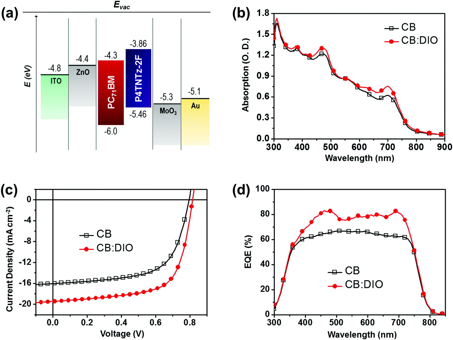 | ||
| Fig. 3 (a) Energy level diagram of the inverted device structure with active materials. (b) UV-vis absorption spectra of P4TNTz-2F (M-MW):PC71BM blend films from CB without DIO and with DIO for a similar thickness of ∼350 nm. (c) J–V curves and (d) EQE spectra of the optimized P4TNTz-2F (M-MW):PC71BM PSCs prepared from CB and CB:DIO. | ||
:PC71BM under standard AM 1.5G illumination
| D:Aa |
Additiveb [DIO] | Thickness [nm] | V OC [mV] | J SC [mA cm−2] | FF [%] | PCEmax (PCEave)c [%] |
|---|---|---|---|---|---|---|
|
a The optimized donor:acceptor ratios were 1:2 (wt:wt%).
b The active layers were deposited from solution in chlorobenzene with DIO (3 vol%).
c The values in parentheses stand for the average PCEs with standard deviations from over 12 devices.
|
||||||
| P4TNTz-2F:PC71BM |
No | 320 | 810 ± 10 | 15.7 ± 0.3 | 62.2 ± 0.8 | 8.1 (7.9 ± 0.1) |
| Yes | 325 | 816 ± 5 | 18.2 ± 0.3 | 66.2 ± 1.4 | 10.1 (9.9 ± 0.2) | |
| Yes | 350 | 813 ± 6 | 19.4 ± 0.5 | 65.5 ± 1.1 | 10.6 (10.3 ± 0.2) | |
| Yes | 390 | 800 ± 14 | 19.1 ± 0.4 | 58.0 ± 0.9 | 9.1 (8.8 ± 0.2) | |
In the optimized 1:2 P4TNTz-2F:PC71BM device prepared without DIO, the VOC reached 0.83 V, with a JSC of 16.04 mA cm−2 and a FF of 61.2%, resulting in a high PCE of 8.07%. The solar cell devices fabricated with processing additives exhibit improved device performances (Table S5, ESI†). Of the various additives tested, namely DIO, diphenyl ether (DPE), and chloronaphthalene (CN), the devices processed with DIO exhibit the highest PCEs (Table S6, ESI†). The P4TNTz-2F:PC71BM solar cells processed with DIO exhibit a high PCE of 10.62% with an open circuit voltage (VOC) of 0.82 V, a short circuit current density (JSC) of 19.45 mA cm−2, and a fill factor (FF) of 66.5%. We found that the optimum thickness of the active layer was 350 nm for PSCs prepared from CB:DIO, which is thicker than that of the PSCs prepared without DIO (≈320 nm).
Note that the photovoltaic parameters of the PSCs prepared from CB:DIO are dependent on the active layer thickness. Increasing the thickness of the active layer prepared from CB:DIO (from 245 to 350 nm) leads to a remarkable increase in JSC (from 15.51 to 19.45 mA cm−2), while moderate FF values up to 66.5% are retained. We suggest that a bicontinuous interpenetrating network of donor and acceptor components is successfully formed in the thick active layer, thereby maximizing light harvesting and enabling the efficient transport of the generated free charge carriers.42 However, further increases in the film thickness over 350 nm led to a decrease in FF (Fig. S16 and Table S6, ESI†), as found in previous studies.9,11 To determine the variation in device performance with the concentration of the DIO additive, we measured the external quantum efficiencies (EQEs) of the optimum devices (Fig. 3d). The substantially broadened EQE responses in the visible region are attributed to the intrinsic absorption region of both P4TNTz-2F and PC71BM. Compared to the EQE value of the device prepared from pure CB, the device prepared from CB:DIO exhibits much higher EQE values over almost the whole of the wavelength region from 350 to 750 nm, with the maximum EQE exceeding 80%. The short-circuit current densities calculated from the integration of the EQE spectra are in good agreement with the trends in the direct J–V measurements (Table S8, ESI†).
To investigate the origin of the high JSC and FF values for thick PSCs, the extents of bimolecular recombination in the active layers were estimated by measuring the dependence of the photocurrent (Jph) on the light intensity (Plight) for the devices processed from CB and CB:DIO (Fig. S18, ESI†).43,44 The logarithmic plots of Jphvs. Plight have linear slopes (α) of 0.973 and 0.996 for the devices prepared from CB and CB:DIO, respectively; the relationship between Jph and Plight can be represented using a power law equation: Jph ∝ (Plight)α, where α is the recombination parameter.45 Since the devices processed from CB:DIO (α = 0.996) have a higher α value than the devices prepared from pure CB (α = 0.973), bimolecular recombination is more suppressed in the active layers processed from CB:DIO than in those processed from CB. This result indicates that the addition of DIO optimizes the nanoscale morphology of the thick BHJ active layers, which results in the efficient separation and transport of charge carriers generated by the absorption of a large amount of incident light by the thick films, which in turn contributes to the high JSC and FF values.
To gain a deeper insight into the effects of the nanoscale morphology of the photoactive layers on the solar cell performances, we used AFM and transmission electron microscopy (TEM). As shown in Fig. 4, the AFM images of the BHJ film prepared from CB:DIO contain nanofibrous surface features with long-range intergrain connectivity, whereas the BHJ film prepared from pure CB has bland and rough surface features. Upon the addition of DIO, well-developed nanowire structures appear; this feature is also present in the neat P4TNTz-2F film. As shown in Fig. S19 (ESI†), the AFM and TEM images of the P4TNTz-2F neat film prepared from CB:DIO show highly crystalline features with densely tangled bundles of PNWs. P4TNTz-2F is completely dissolved in the blending solutions at elevated temperatures (≈70 °C), so the features in the AFM images of the blend films originate from the kinetic and thermodynamic parameters of film formation, which significantly affect the crystal formation and aggregation of the polymer domains.23,46 The formation of PNWs is attributed to the prolonged evolution time of the crystals, which arises from the reduced solvent evaporation rate of the processing solvent due to the high boiling point of DIO.46 These results are corroborated by the enhanced intermolecular π–π* transition peaks in the UV-vis spectra of the blend polymer films with DIO (Fig. 3b and Fig. S20, ESI†).
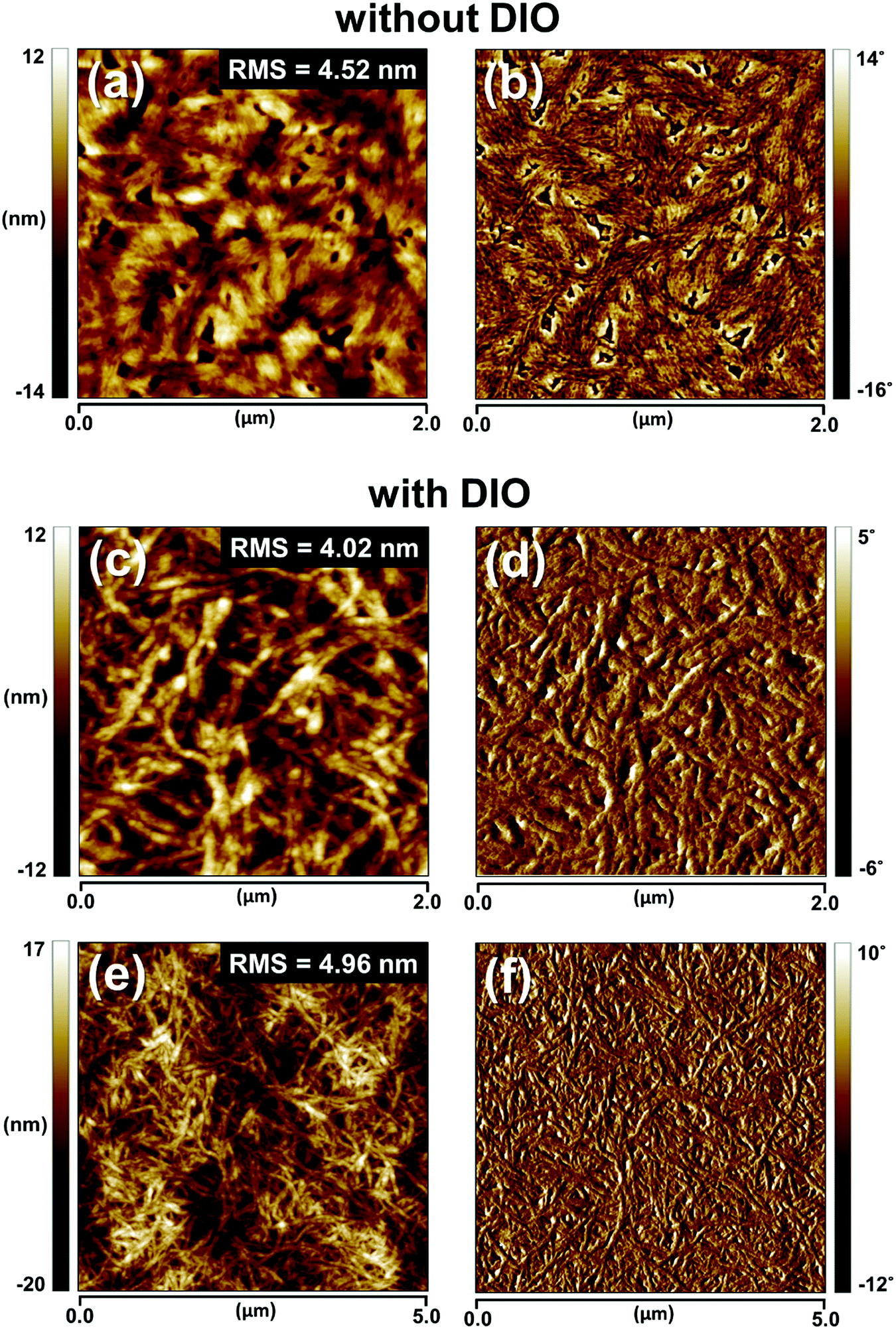 | ||
| Fig. 4 TM-AFM topography images (left row) and phase images (right row) of 1:2 P4TNTz-2F (M-MW):PC71BM blend films on the actual devices prepared from CB without DIO (a and b) and with 3 vol% DIO (c–f). | ||
The TEM images of the blend films provide further insights into the morphological development of the BHJ films (Fig. 5, Fig. S21, and Fig. S22, ESI†). Interestingly, the internal morphology of the blend film prepared from pure CB (Fig. 5a) is slightly different from its surface topography, as shown in the AFM image. The TEM image reveals that the BHJ films prepared from pure CB possess densely distributed polymer nanofibrils with larger and strongly deviating widths (≈14 ± 4 nm). In contrast, the BHJ films prepared from CB:DIO contain clear polymer nanowire structures that have widths of approximately 6 ± 1 nm and lengths of a few hundreds of nanometers (Fig. 5b). We infer that DIO prevents large-scale phase separation in the M-MW P4TNTz-2F blend films. When spin-casting P4TNTz-2F:PC71BM from a warm solvent mixture of CB and DIO, the majority of CB quickly evaporates and a DIO-saturated solution is left behind. Since DIO selectively dissolves PC71BM, the PC71BM molecules are likely to integrate into the polymer (P4TNTz-2F) aggregates during film formation, which results in a nanoscale interpenetrating network with crystalline ordered PNWs, as is desirable for the active layers of BHJ PSCs.47 The narrow PNWs (≈6 nm) of P4TNTz-2F prepared from CB:DIO are beneficial to exciton dissociation and charge generation because the typical exciton diffusion length of conjugated polymers is a few nanometers.48 Indeed, the photoluminescence (PL) quenching efficiencies (QPL) of the P4TNTz-2F:PC71BM films prepared from CB:DIO exceed 98%, which indicates that very efficient exciton dissociation arises at the donor–acceptor interface (Fig. 5e and Fig. S23, ESI†). Furthermore, the nanowire crystals of P4TNTz-2F have a long-range π-connectivity on a scale of a few hundred nanometers, which will enhance the charge carrier transport properties of the thick active layers of optimized PSCs, and lead to a high JSC value.
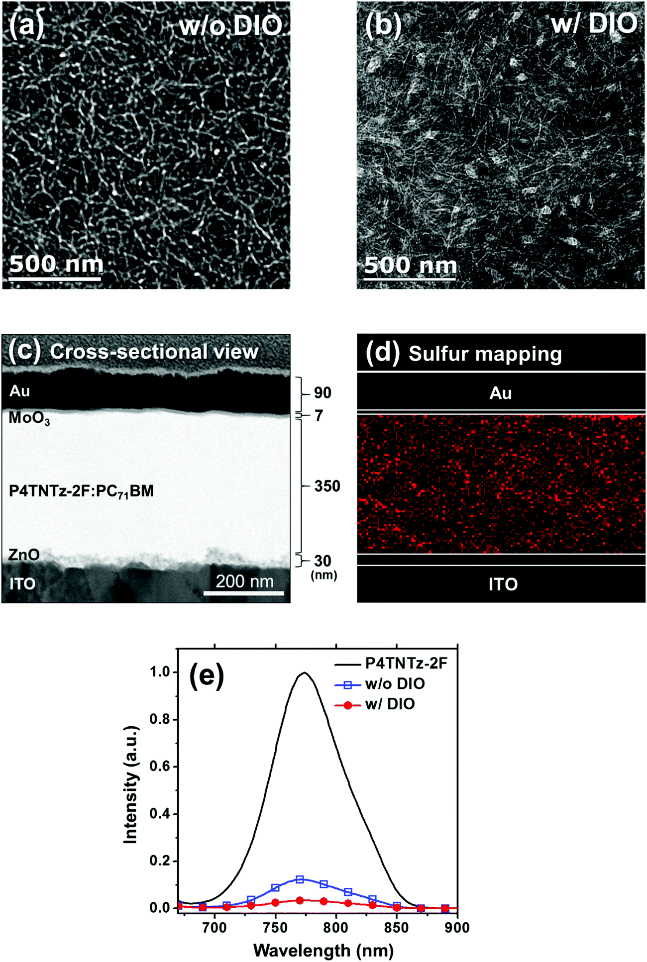 | ||
| Fig. 5 TEM images of the P4TNTz-2F (M-MW):PC71BM blend films on the actual optimum devices prepared from CB (a) without DIO and (b) with 3 vol% DIO. (c) Cross-sectional TEM images and (d) EDS sulfur mapping of optimum devices prepared from CB:DIO. (e) Photoluminescence spectra of the blend films based on P4TNTz-2F (M-MW):PC71BM without DIO and with DIO (3 vol%). The films were excited at a wavelength of 697 nm. Each spectrum was corrected for the absorption of the film at the excitation wavelength. | ||
Fig. 5c and d show the cross-sectional TEM images and energy dispersive X-ray spectroscopy (EDS) results for the optimum devices prepared from CB:DIO. The component layers and their thicknesses in the devices can be clearly seen in Fig. 5c. We performed EDS sulfur (S) mapping of cross-sections of the BHJ films to investigate the vertical distributions of the P4TNTz-2F polymer chains (Fig. 5d). In the EDS S mapping images, the BHJ film prepared from CB:DIO contains a continuous and evenly distributed polymer network from the bottom ZnO layer to the top MoO3 layer. This optimized vertical morphology promotes hole and electron charge carrier transport along the respective pathways of P4TNTz-2F and PC71BM in the vertical direction, which contributes to the high FF and JSC values of the thick films.
Since the crystallinity and the molecular orientation of the polymers are important parameters to determine the charge transport properties in PSCs, GIXD was utilized for the blend films (Fig. 6 and Fig. S24, ESI†). The diffraction patterns collected from the P4TNTz-2F:PC71BM blend films reveal dramatic changes in the molecular orientations of the polymers upon the addition of DIO: the in-plane lamellar diffraction peaks intensify (Fig. 6b), indicating that the polymer crystallites tend to adopt a face-on orientation upon DIO treatment,37,49–51 which is beneficial for the vertical charge transportation in the solar cell devices. Therefore, the observed changes in the molecular orientation of the polymers in the blend films contribute to high JSC and FF values. As shown in Fig. 6c, the blend films prepared with DIO retain the (002) reflection along the qxy axis, as is the case for the neat polymer films, which is possibly induced by the formation of polymer nanowire crystallites.
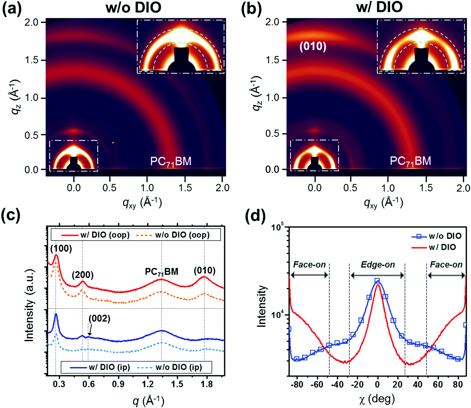 | ||
| Fig. 6 Two-dimensional GIXD images of the P4TNTz-2F (M-MW):PC71BM blend films prepared from CB (a) without DIO (w/o DIO) and (b) with 3 vol% DIO (w/ DIO). (c) qz (out-of-plane, oop) and qxy (in-plane, ip) scans of GIXD from the blend films. (d) Pole figures extracted from the lamellar diffraction for the blend films. | ||
We also carried out GIXD measurements with various incident angles (αi = 0.10, 0.13, and 0.15°) for the optimized thick active layers (Fig. S25, ESI†), where the X-rays with an incident angle of 0.10° (αi < critical angle of the film) are diffracted in the near-surface region of the film and the X-rays with an incident angle of 0.15° (critical angle of the film < αi < critical angle of the substrate) penetrate the whole film thickness and thus produce diffractions in the bulk of the film.27 When the diffractions are measured at an αi of 0.10°, it can be seen that the P4TNTz-2F polymer crystals in the blend films prepared from both CB and CB:DIO predominantly adopt an edge-on orientation. However, in the case of the blend films prepared from CB:DIO, the diffractions of the polymers are stronger, which is probably due to the formation of polymer nanowire structures on the top surface of the films, as confirmed by the AFM images (Fig. 4c); in general, most conjugated polymers possess an edge-on configuration in the presence of nanowire structures.14–20,23 In contrast, the diffractions of the blend films prepared from CB:DIO as measured at an αi of 0.15° contain bimodal features due to both edge-on and face-on crystallites. We infer that, in addition to the polymer nanowires, other coexisting polymer matrices are present, which possess a face-on orientation.
To further investigate the polymer orientation, we performed a pole figure analysis for the blend films by using the azimuthal angle scans of the lamellar (100) reflections, as shown in Fig. 6d (see the insets for close-ups of the lamellar diffractions). Since the intensities of the peaks near χ = 0° and χ = ±90° are related to the edge-on and face-on orientations of the crystallites, respectively,7,27 the fractions of the polymer orientations can be calculated directly from the intensity ratios. The ratio of face-on to edge-on orientations for the blend film prepared from CB:DIO is much higher than that for the blend film prepared from pure CB. It is noteworthy that although the fraction of face-on polymer crystallites significantly increases after DIO treatment, the strong intensity of the edge-on polymer crystallites is retained when compared to the blend film from pure CB.
Charge carrier transport in the blend films in the direction perpendicular to the substrate plane was investigated by using the space-charge limited current (SCLC) model. Hole-only (ITO/MoO3/P4TNTz-2F:PC71BM/MoO3/Au) and electron-only (Al/P4TNTz-2F:PC71BM/LiF/Al) diodes were prepared by using optimized BHJ films. The resulting hole and electron mobilities are shown in Fig. S28 and are summarized in Table S10 (ESI†). The hole (μh) and electron mobilities (μe) obtained from the SCLC measurements are 8.31 × 10⁻³ cm2 V−1 s−1 and 4.53 × 10⁻³ cm2 V−1 s−1 respectively for the devices prepared from CB:DIO, and 1.98 × 10⁻³ cm2 V−1 s−1 and 2.77 × 10⁻³ cm2 V−1 s−1 respectively for the devices prepared from CB. Importantly, the devices processed from CB:DIO exhibit considerably higher μh values than the devices prepared from CB, which is probably due to PNW formation and the face-on polymer orientation. The improved μe and well-balanced μh/μe ratio (1.83) are important contributors to the high FF of the CB:DIO-processed devices. The high μe of the blend film processed from CB:DIO is supported by the GIXD results, which show that the intensity of the isotropic peak at q ≈ 1.33Å, which corresponds to PC71BM aggregates, becomes higher upon the addition of DIO. Thus, DIO significantly enhances the aggregation of PC71BM, which in turn contributes to increased crystallinity and electron mobility. These results for the vertical charge carrier mobility are in good agreement with the BHJ morphology of the thick blend films prepared from CB:DIO, which possess bicontinuous interpenetrating donor/acceptor networks containing PNWs (Fig. 5b and d), polymer crystallites in the face-on orientation (Fig. 6b), and enhanced PC71BM aggregation/crystallinity that results in high JSC and FF values for the solar cell devices.
Conclusions
We have obtained PCE values reaching 10% in single-junction PSCs with an inverted architecture by using a D–A conjugated polymer (P4TNTz-2F) as the p-type material and PC71BM as the n-type material. P4TNTz-2F has a low bandgap and a deep-lying HOMO level, which results in solar cells with high levels of light harvesting and a high VOC. The tailored chemical structure of P4TNTz-2F with its highly rigid/coplanar backbone conformation and facile solution-processability results in the formation of highly crystalline PNWs in BHJ PSCs. The high PCE is most probably due to the presence of highly ordered PNWs with the appropriate spatial density and dimensions and the favorable face-on orientation of P4TNTz-2F in the active layer, which facilitates charge transport and reduces charge recombination. Remarkably, these results were achieved with thick active layers (≈350 nm), which is particularly beneficial for practical applications.Acknowledgements
J. Lee and D. H. Sin contributed equally to this work. This work was supported by a grant (Code no. 2011-0031628) from the Center for Advanced Soft Electronics under the Global Frontier Research Program of the Ministry of Science, ICT & Future Planning, Korea. The authors thank the Pohang Accelerator Laboratory for providing the synchrotron radiation sources at 9A beamline used in this study.Notes and references
- G. Yu, J. Gao, J. C. Hummelen, F. Wudl and A. J. Heeger, Science, 1995, 270, 1789 CAS.
- A. C. Arias, J. D. MacKenzie, I. McCulloch, J. Rivnay and A. Salleo, Chem. Rev., 2010, 110, 3 CrossRef CAS PubMed.
- G. Dennler, M. C. Scharber and C. J. Brabec, Adv. Mater., 2009, 21, 1323 CrossRef CAS.
- S. B. Darling and F. You, RSC Adv., 2013, 3, 17633 RSC.
- T. Liu, J. Zhao, Z. Li, C. Mu, W. Ma, H. Hu, K. Jiang, H. Lin, H. Ade and H. Yan, Nat. Commun., 2014, 5, 5293 CrossRef PubMed.
- J. Zhao, Y. Li, G. Yang, K. Jiang, H. Lin, H. Ade, W. Ma and H. Yan, Nat. Energy, 2016, 1, 15027 CrossRef.
- V. Vohra, K. Kawashima, T. Kakara, T. Koganezawa, I. Osaka, K. Takimiya and H. Murata, Nat. Photonics, 2015, 9, 403 CrossRef CAS.
- J. Gao, L. Dou, W. Chen, C.-C. Chen, X. Guo, J. You, B. Bob, W.-H. Chang, J. Strzalka, C. Wang, G. Li and Y. Yang, Adv. Energy Mater., 2014, 4, 1300739 CrossRef.
- W. Li, K. H. Hendriks, W. S. C. Roelofs, Y. Kim, M. M. Wienk and R. A. J. Janssen, Adv. Mater., 2013, 25, 3182 CrossRef CAS PubMed.
- Z. Chen, P. Cai, J. Chen, X. Liu, L. Zhang, L. Lan, J. Peng, Y. Ma and Y. Cao, Adv. Mater., 2014, 26, 2586 CrossRef CAS PubMed.
- H. Choi, S.-J. Ko, T. Kim, P.-O. Morin, B. Walker, B. H. Lee, M. Leclerc and J. Y. Kim, Alan J. Heeger, Adv. Mater., 2015, 27, 3318 CrossRef CAS PubMed.
- J. S. Kim, J. H. Lee, J. H. Park, C. Shim, M. Sim and K. Cho, Adv. Funct. Mater., 2011, 21, 480 CrossRef CAS.
- J.-H. Kim, J. H. Park, J. H. Lee, J. S. Kim, M. Sim, C. Shim and K. Cho, J. Mater. Chem., 2010, 20, 7398 RSC.
- D. H. Kim, D. Y. Lee, H. S. Lee, W. H. Lee, Y. H. Kim, J. I. Han and K. Cho, Adv. Mater., 2007, 19, 678 CrossRef CAS.
- S. Wang, M. Kappl, I. Liebewirth, M. Müller, K. Kirchhoff, W. Pisula and K. Müllen, Adv. Mater., 2012, 24, 417 CrossRef CAS PubMed.
- H. A. Um, D. H. Lee, D. U. Heo, D. S. Yang, J. Shin, H. Baik, M. J. Cho and D. H. Choi, ACS Nano, 2015, 9, 5264 CrossRef CAS PubMed.
- S. B. Jo, W. H. Lee, L. Qiu and K. Cho, J. Mater. Chem., 2012, 22, 4244 RSC.
- D. M. O'Carroll, C. E. Petoukhoff, J. Kohl, B. Yu, C. M. Carter and S. Goodman, Polym. Chem., 2013, 4, 5181 RSC.
- H. Xin, F. S. Kim and S. A. Jenekhe, J. Am. Chem. Soc., 2008, 130, 5424 CrossRef CAS PubMed.
- H. Yan, Y. Song, G. R. McKeown, G. D. Scholes and D. S. Seferos, Adv. Mater., 2015, 27, 3484 CrossRef CAS PubMed.
- Y. J. Cheng, S. H. Yang and C. S. Hsu, Chem. Rev., 2009, 109, 5868 CrossRef CAS PubMed.
- J. Cao, Q. Liao, X. Du, J. Chen, Z. Xiao, Q. Zuo and L. Ding, Energy Environ. Sci., 2013, 6, 3224 CAS.
- J. Lee, S. B. Jo, M. Kim, H. G. Kim, J. Shin, H. Kim and K. Cho, Adv. Mater., 2014, 26, 6706 CrossRef CAS PubMed.
- D. H. Kim, J. Mei, A. L. Ayzner, K. Schmidt, G. Giri, A. L. Appleton, M. F. Toney and Z. Bao, Energy Environ. Sci., 2014, 7, 1103 CAS.
- T. L. Nguyen, H. Choi, S.-J. Ko, M. A. Uddin, B. Walker, S. Yum, J.-E. Jeong, M. H. Yun, T. J. Shin, S. Hwang, J. Y. Kim and H. Y. Woo, Energy Environ. Sci., 2014, 7, 3040 CAS.
- H. J. Son, W. Wang, T. Xu, Y. Liang, Y. Wu, G. Li and L. Yu, J. Am. Chem. Soc., 2011, 133, 1885 CrossRef CAS PubMed.
- J. W. Jo, J. W. Jung, E. H. Jung, H. Ahn, T. J. Shin and W. H. Jo, Energy Environ. Sci., 2015, 8, 2427 CAS.
- I. Osaka, M. Shimawaki, H. Mori, I. Doi, E. Miyazaki, T. Koganezawa and K. Takimiya, J. Am. Chem. Soc., 2012, 134, 3498 CrossRef CAS PubMed.
- M. Wang, X. Hu, P. Liu, W. Li, X. Gong, F. Huang and Y. Cao, J. Am. Chem. Soc., 2011, 133, 9638 CrossRef CAS PubMed.
- K. Kawashima, I. Osaka and K. Takimiya, Chem. Mater., 2015, 27, 6558 CrossRef CAS.
- Z. Zhang, F. Lin, H.-C. Chen, H.-C. Wu, C.-L. Chung, C. Lu, S.-H. Liu, S.-H. Tung, W.-C. Chen, K.-T. Wong and P.-T. Chou, Energy Environ. Sci., 2015, 8, 552 CAS.
- Y.-X. Xu, C.-C. Chueh, H.-L. Yip, F.-Z. Ding, Y.-X. Li, C.-Z. Li, X. Li, W.-C. Chen and A. K.-Y. Jen, Adv. Mater., 2012, 24, 6356 CrossRef CAS PubMed.
- A. C. Stuart, J. R. Tumbleston, H. Zhou, W. Li, S. Liu, H. Ade and W. You, J. Am. Chem. Soc., 2013, 135, 1806 CrossRef CAS PubMed.
- B. C. Schroeder, Z. Huang, R. S. Ashraf, J. Smith, P. D’Angelo, S. E. Watkins, T. D. Anthopoulos, J. R. Durrant and I. McCulloch, Adv. Funct. Mater., 2012, 22, 1663 CrossRef CAS.
- J. A. Bartelt, J. D. Douglas, W. R. Mateker, A. E. Labban, C. J. Tassone, M. F. Toney, J. M. J. Fréchet, P. M. Beaujuge and M. D. McGehee, Adv. Energy Mater., 2014, 4, 1301733 CrossRef.
- C. J. Brabec, A. Cravino, D. Meissner, N. S. Sariciftci, T. Fromherz, M. T. Rispens, L. Sanchez and J. C. Hummelen, Adv. Funct. Mater., 2001, 11, 374 CrossRef CAS.
- J. Lee, R. Singh, D. H. Sin, H. G. Kim, K. C. Song and K. Cho, Adv. Mater., 2016, 28, 69 CrossRef CAS PubMed.
- H. G. Kim, B. Kang, H. Ko, J. Lee, J. Shin and K. Cho, Chem. Mater., 2015, 27, 829 CrossRef CAS.
- T. Lei, Y. Cao, X. Zhou, Y. Peng, J. Bian and J. Pei, Chem. Mater., 2012, 24, 1762 CrossRef CAS.
- M. Brinkmann, E. Gonthier, S. F. Bogen, K. Tremel, S. Ludwigs, M. Hufnagel and M. Sommer, ACS Nano, 2012, 6, 10319 CrossRef CAS PubMed.
- I. Osaka, M. Saito, H. Mori, T. Koganezawa and K. Takimiya, Adv. Mater., 2012, 24, 425 CrossRef CAS PubMed.
- H.-C. Liao, C.-S. Tsao, Y.-T. Shao, S.-Y. Chang, Y.-C. Huang, C.-M. Chuang, T.-H. Lin, C.-Y. Chen, C.-J. Su, U.-S. Jeng, Y.-F. Chen and W.-F. Su, Energy Environ. Sci., 2013, 6, 1938 CAS.
- L. Lu, T. Xu, W. Chen, E. S. Landry and L. Yu, Nat. Photonics, 2014, 8, 716 CrossRef CAS.
- Z. Li, J. D. A. Lin, H. Phan, A. Sharenko, C. M. Proctor, P. Zalar, Z. Chen, A. Facchetti and T.-Q. Nguyen, Adv. Funct. Mater., 2014, 24, 6989 CrossRef CAS.
- S. R. Cowan, J. Wang, J. Yi, Y. J. Lee, D. C. Olson and J. W. P. Hsu, J. Appl. Phys., 2013, 113, 154504 CrossRef.
- H.-C. Liao, C.-C. Ho, C.-Y. Chang, M.-H. Jao, S. B. Darling and W.-F. Su, Mater. Today, 2013, 16, 326 CrossRef CAS.
- S. J. Lou, J. M. Szarko, T. Xu, L. Yu, T. J. Marks and L. X. Chen, J. Am. Chem. Soc., 2011, 133, 20661 CrossRef CAS PubMed.
- D. E. Markov, E. Amsterdam, P. W. M. Blom, A. B. Sieval and J. C. Hummelen, J. Phys. Chem. A, 2005, 109, 5266 CrossRef CAS PubMed.
- D. H. Kim, A. L. Ayzner, A. L. Appleton, K. Schmidt, J. Mei, M. F. Toney and Z. Bao, Chem. Mater., 2013, 25, 431 CrossRef CAS.
- J. Zhao, S. Zhao, Z. Xu, B. Qiao, D. Huang, L. Zhao, Y. Li, Y. Zhu and P. Wang, ACS Appl. Mater. Interfaces, 2016, 8, 18231 CAS.
- W. Chen, T. Xu, F. He, W. Wang, C. Wang, J. Strzalka, Y. Liu, J. Wen, D. J. Miller, J. Chen, K. Hong, L. Yu and S. B. Darling, Nano Lett., 2011, 11, 3707 CrossRef CAS PubMed.
Footnotes |
| † Electronic supplementary information (ESI) available. See DOI: 10.1039/c6ee02466a |
| ‡ These authors contributed equally to this work. |
| This journal is © The Royal Society of Chemistry 2017 |