
 Open Access Article
 This Open Access Article is licensed under a Creative Commons Attribution-Non Commercial 3.0 Unported Licence
Active optical modulation in hybrid transparent-conductive oxide/electro-optic multilayers
Riccardo Magrin
Maffei†
 ab,
Michele
Magnozzi†
c,
Maria
Sygletou
c,
Stefano
Colace
c,
Sergio
D’Addato
ab,
Alexandr Yu.
Petrov
d,
Maurizio
Canepa
c,
Piero
Torelli
d,
Alessandro
di Bona
b,
Stefania
Benedetti
*b and
Francesco
Bisio
e
ab,
Michele
Magnozzi†
c,
Maria
Sygletou
c,
Stefano
Colace
c,
Sergio
D’Addato
ab,
Alexandr Yu.
Petrov
d,
Maurizio
Canepa
c,
Piero
Torelli
d,
Alessandro
di Bona
b,
Stefania
Benedetti
*b and
Francesco
Bisio
e
aDipartimento di Scienze Fisiche, Informatiche, Matematiche, Università di Modena e Reggio Emilia, via Campi 213/a, 41125, Modena, Italy
bCNR–Istituto Nanoscienze, via Campi 213/a, 41125, Modena, Italy. E-mail: stefania.benedetti@nano.cnr.it
cOptMatLab, Dipartimento di Fisica, Università di Genova, Via Dodecaneso 33, 16146 Genova, Italy
dCNR-IOM, Laboratorio TASC, AREA Science Park, Basovizza, 34149 Trieste, Italy
eCNR-SPIN, C.so Perrone 24, 16152 Genova, Italy
First published on 5th February 2025
Abstract
We report the room temperature, low-voltage-enabled modulation of the optical response of hybrid transparent-conductive-oxide/ferroelectric multilayers. We have fabricated an optical multilayer consisting of Al-doped ZnO (AZO) and BaTiO3 films deposited on a Nb-doped SrTiO3(110) substrate. Applying a low voltage between the AZO film and the substrate, a significant variation of the system's optical response has been detected by means of in operando spectroscopic ellipsometry. The voltage-induced variations have been ascribed to a combination of charge accumulation/depletion at the insulator/semiconductor interface and the field-induced Pockels effect in the BaTiO3 layer and successfully reproduced by an optical model including these effects. We have deduced a variation of the refractive index in AZO in the infrared range by more than 0.1 at an applied bias of 0.2 V and by more than 2 at an applied bias of just 3 V at room temperature, which can be strongly appealing for voltage-modulated active optical systems.
Introduction
Transparent conductive oxides (TCOs) are a class of materials that display optical transmittance in excess of 80% combined with electrical resistance as low as 10−4 Ω cm, making them appealing for applications in photovoltaics and optoelectronics.1–4 In particular, the ability to adjust the free carrier concentration through the doping level and the low losses allows epsilon-near-zero conditions to be tuned in visible light communications and infrared (IR) telecommunication windows.5–7 While the tuning of the electrical and optical properties of these materials by modulating their intrinsic properties (like film thickness,8,9 or dopant concentration10,11) is extensively exploited, a great challenge is their control by external stimuli, which would pave the way for intriguing applications in photonic devices.The most flexible and appealing method to perform optical modulation is to exploit the field effect (FE) by applying an external bias to TCO thin films within a suitable metal–oxide–semiconductor (MOS) device.12 The electrical gating method is simple and can be a viable approach to achieve new functionalities in optoelectronic and photonic devices analogous to field-effect transistors.13,14 Through FE, large permittivity variations can be obtained in TCOs because of their largely inferior carrier density with respect to classic conductors like noble metals.
Following the application of an external electric field, an ultrathin accumulation/depletion layer is formed at the dielectric/conducting oxide interface.15–19 The injection or depletion of charges within this ultrathin layer may change the local refractive index by as much as a unity, as observed for example at the dielectric/indium–tin oxide (ITO) interface.15 At present, the vast majority of the studies concerning the FE-tuning of the dielectric properties of TCOs and their applications are focused on ITO-based systems,20–23 whereas much less attention has been dedicated to alternative materials, like Al-doped ZnO (AZO),12,24–26 which are based on earth-abundant materials and are therefore far cheaper and more sustainable than ITO. From the point of view of active photonics applications, both materials show analogous behavior, keeping in mind that the charge injection/depletion phenomenon due to the field effect critically depends on the doping level of the TCO.
In a previous publication, we have demonstrated the FE-gating of AZO films,12 albeit in a configuration (a plane capacitor with a 500 μm-thick SrTiO3 dielectric) requiring a high-voltage bias and cryogenic temperatures to achieve a sizable charge displacement. Reducing the insulator thickness by exploiting a thin film of a high-k dielectric, like BaTiO3 (BTO), should easily allow boosting the charge-density modulation by increasing the capacitance of the system, allowing lower bias and room temperature operation, with relevant applicative consequences. The BTO crystal structure lacks inversion symmetry and shows a large Pockels electro-optic effect, a linear variation of the refractive index in response to an applied electric field. Furthermore, BTO is also CMOS compatible for electro-optic modulators.27
In this work, we report the investigation of FE-induced modulation of the optical response of micro-capacitors constituted by epitaxial AZO/BTO/Nb:STO (NSTO) multilayer stacking. Changes in the dielectric function have been observed via in operando spectroscopic ellipsometry (SE), in a photon energy range spanning in the visible and near-infrared range (NIR, 0.73–3.22 eV), while the electrical response of the capacitors has been characterized by impedance analysis. Applying a bias to an AZO/BTO capacitor results in the creation of an accumulation/depletion zone at the AZO/BTO and BTO/NSTO interfaces, depending on the sign of the applied potential, accompanied by the field-induced Pockels effect in BTO. This leads to sizable voltage-induced variations of the optical response of the device that we interpreted through the modeling of field-induced variations of the dielectric permittivity of the AZO, NSTO and BTO films. We took advantage of the extreme sensitivity of SE to thin-film properties in order to observe the voltage-induced variation of the optical response of the system. Furthermore, we were able to understand how the material's optical properties changed with the bias. We did this by modeling the charge profile of the accumulation/depletion layers at the AZO/BTO and BTO/NSTO interfaces, and thus quantifying the bias-induced variations in the dielectric response of the system.
Experimental
AZO/BTO/NSTO capacitors and Hall probes were fabricated using a two-step process consisting in (i) the epitaxial growth of BTO and (ii) the microfabrication of the top electrode and conductors using a combination of lithography processes and thin film deposition using magnetron sputtering. The choice for the SrTiO3(110) substrate is motivated by the intention to induce the epitaxial growth of all the layers thanks to the small lattice mismatch, reduce defects in the BTO dielectric layer,28,29 and improve the electrical response in AZO.30–32The first step is the deposition of a 170 nm thick BTO film onto a conductive 0.5 wt% Nb-doped SrTiO3(110) bulk substrate via layer-by-layer molecular beam epitaxy (MBE).33 This has been performed by evaporation of Ba and Ti in an oxygen atmosphere at a pressure of 2 × 10⁻⁶ mbar. The quality of the epitaxial film, deposited at 750 °C, has been monitored through reflection high-energy electron diffraction (RHEED) during the growth, with a deposition rate of approximately one unit cell per minute and checked after deposition by X-ray diffraction.
The second step is the microfabrication of the capacitors, which is accomplished by several lithographic processes. Electron beam lithography is performed using a Zeiss Sigma scanning electron microscope and a Raith ELPHY quantum pattern generator. Details on thin film deposition and lithography processes are given below. A capacitor stack, as shown in Fig. 1a and b, is composed of the conductive Nb:SrTiO3(110) substrate acting as a common back-electrode, the BTO film serving as the dielectric, and the AZO film on top as the active electrode.
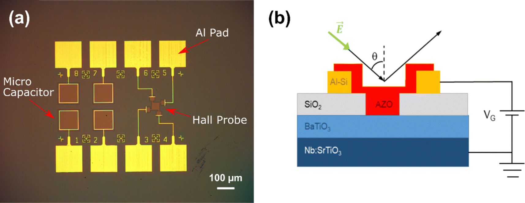 | ||
| Fig. 1 (a) View under an optical microscope of the microcapacitors fabricated via EBL. (b) Cross-section of the stacking of the layer films in the microcapacitor of panel a. | ||
First, an insulating, 100 nm thick SiO2 layer with square openings which both defines the top electrode and provides mechanical support for the conductors and bonding pads is deposited on the BTO film by RF magnetron sputtering (3′′ SiO2 target, 120 W at room temperature), followed by the lift-off process. To achieve the ideal balance between capacitor leakage current and beam size for SE measurements, devices with diverse capacitor sizes and shapes were evaluated. The second process is the fabrication of the wires, made of 100 nm thick sputtered Nb patterned by lift-off (DC sputtering, 70 W, Nb 3′′ target, 99.99%). To create the Al–Si bonding pads, a combination of DC magnetron sputtering and lift-off is employed, depositing 5 nm Cr and 500 nm Al–Si layers (Cr 4′′ target, 125 W DC, Al/Si 1 wt% 4′′ target, 500 W DC). The fabrication of the AZO top electrode involves co-sputtering at room temperature from ZnO and Al targets (3′′ target, purity 99.99%, RF and DC, respectively) in a 5 mTorr Ar working pressure, resulting in a 250 nm thick AZO film and a further lift-off process defines the shape of the electrode. A precise balance of RF and DC power is crucial for achieving the optimal doping concentration of 4 at% in the material. Energy dispersive X-ray spectroscopy (EDX) analysis using an FEI Quanta-200 ESEM verifies the successful doping optimization. The epitaxial growth of AZO, facilitated by the substrate's structure,30,31 optimizes the electrical properties of films.32 The film thickness was monitored in situ using a quartz microbalance and validated using a stylus profilometer. The final fabrication step involves wire bonding to a PCB plate.
The capacitance of the devices was determined using a high-precision Agilent 4294A impedance analyzer, spanning a frequency range of 100 Hz to 30 MHz. Standard Hall and Van der Pauw measurements were also performed on a probe specifically fabricated next to the capacitors to accurately assess the DC electrical properties of the AZO film, namely resistivity, charge carrier concentration, and mobility (Fig. 1a).
The optical response of the system in its unbiased state and following the bias-induced charge injection/depletion has been investigated by means of in operando spectroscopic ellipsometry (SE) versus an applied gate voltage in the range of ±3 V. SE measurements were performed by means of a J. A.Woollam M-2000 ellipsometer (0.73–5 eV (245–1700 nm) spectral range) with home-designed optical micro-probes, allowing ellipsometry spectra to be recorded over areas of around 100 μm in lateral size. The SE acquisition range was limited to the 0.73–3.22 eV interval during in operando acquisitions by inserting a longpass-wavelength filter, in order to avoid the presence of any photoinduced carriers in the AZO film. The incidence angle was 55° for all measurements. SE returns the so-called ellipsometric angles Ψ(λ) and Δ(λ), defined through the equation:
rp/rs = tan![[thin space (1/6-em)]](https://www.rsc.org/images/entities/char_2009.gif) Ψ·eiΔ Ψ·eiΔ |
Results and discussion
Unbiased system
AZO/BTO/NSTO capacitors and Hall probes fabricated using the procedure discussed in the previous section have NSTO acting as a back-electrode for the microcapacitor, BTO as the dielectric and AZO as the active electrode, respectively, and are shown in Fig. 1.First, the BTO film has been grown epitaxially on the NSTO(110) substrate. XRD is used to probe the structural characteristics, including the quality and orientation, of the epitaxial BTO film grown on the NSTO(110) substrate. As shown in Fig. 2, the BTO film grows with a (110) surface orientation on the NSTO(110) substrate, consistent with the small lattice mismatch between the two perovskite materials.
 | ||
| Fig. 2 2θ–ω scan of the BTO film grown on NSTO(110). | ||
The AZO film deposited on BTO exhibited a resistivity ρ of 3.2 × 10⁻³ Ω cm, a carrier density N0 of 2.1 × 1020 cm−3 and an electrical Hall mobility μ of 9.1 cm2 (V s)−1, as measured by the probe fabricated near to the capacitors.
The capacitance and leakage currents of the capacitors were determined using precision impedance measurements (Fig. 3). The experimental data were effectively modeled by an equivalent circuit (the inset of Fig. 3b) comprising the capacitance of the BTO capacitor (CBTO) in parallel with a resistance due to the leakage current (RBTO) in BTO, both connected in series with a resistance (RAZO) representing the finite resistance of the AZO electrode and NSTO back-electrode, and finally in parallel with a capacitance (CP) attributed to the electrical connections, namely the wires and bonding pads.
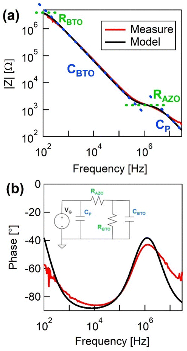 | ||
| Fig. 3 Impedance measurements of the MOS capacitor. (a) Absolute value |Z| and (b) phase of the impedance (measure – red line; model – black line). | ||
The impedance magnitude (|Z|, Fig. 3a) shows the onset of a low-frequency plateau (<1 kHz) due to the leak resistance of BTO, followed by a capacitive regime up to 100 kHz. The plateau around 1 MHz represents the resistive behavior of AZO and NSTO plates, while the high-frequency region (>10 MHz) is again capacitive due to the capacitance of wires and pads. Modeling reveals RBTO ≈ 5 MΩ, CBTO ≈ 220 pF, RAZO ≈ 1.7 kΩ, and CP ≈ 30 pF. Assuming an ideal parallel plate capacitor, the relative dielectric constant of the BTO film (εBTO) is estimated to be εBTO ≈ 235. Despite its simplified assumptions, the model effectively captures the essential behavior of the system, particularly in the 1 kHz to 100 kHz capacitive region dominated by CBTO.
The ellipsometry measurements of the unbiased capacitor are shown in Fig. 4a (markers). The interpretation of those data leaned on the measurements of the optical response of every individual component of the system, namely the NSTO substrate, and the individually and independently grown BTO and AZO layers, in order to have available reference values of the dielectric functions of the component layers before modeling their behavior in the NSTO/BTO/AZO stack. We therefore first measured the bare NSTO substrate and the BTO/NSTO system before the fabrication of the microcapacitors. We then proceeded to measure the full AZO/BTO/NSTO system in the unbiased state. In order to model the dielectric functions of NSTO, BTO and AZO, we resorted to a superposition of oscillators whose functional form accounts for the different electronic contributions to the optical response.35 In particular, so-called PSEMI oscillators were employed to model the interband transitions, whereas a Drude contribution was introduced into the NSTO and AZO layers to account for the doping-induced free-electron contribution.36,37 For the SE modeling, we used WVASE software (J. A.Woollam, Co.).
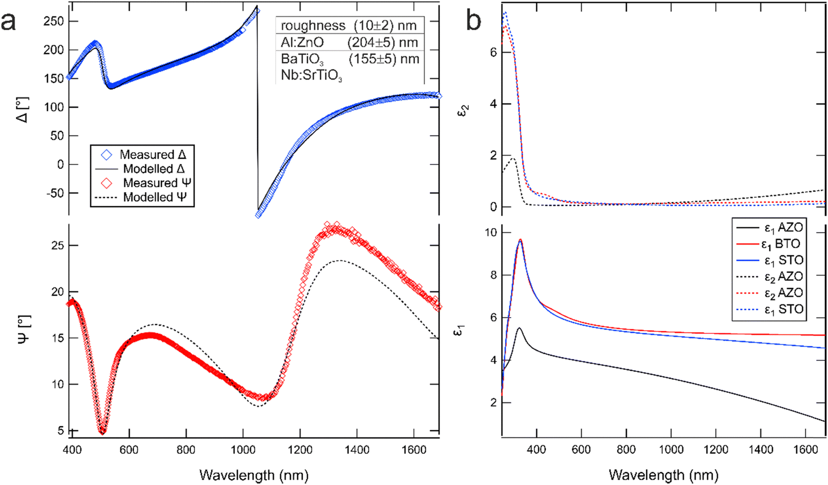 | ||
| Fig. 4 (a) Measured and modelled ellipsometric angles Δ and Ψ for the capacitor without the bias. (b) Real and imaginary parts of the dielectric function of every layer of the capacitor as extracted from ellipsometry. | ||
The dielectric functions of each layer of the system are reported in Fig. 4b. For all the materials, the dielectric functions are characterized by a transparent region across the visible and near-infrared range and by interband transitions below 350 nm, in the near UV. NSTO and AZO exhibit a Drude contribution in the NIR range, due to their doping. The dielectric functions are in very good agreement with the literature, both for AZO and for NSTO and BTO.35,38 The best fit between the model (lines in Fig. 4a) and the experimental data for the full AZO/BTO/NSTO system was found for a BTO layer thickness of (160 ± 5) nm, an AZO layer thickness of (205 ± 5) nm and a surface roughness just below 10 nm. The angular spread due to the focussing of the ellipsometer beam was duly taken into account. In the fitting procedure, the NSTO and the BTO dielectric functions obtained from the bare-substrate data and BTO/NSTO SE measurements were left unchanged, and the only fitting parameters were the thickness of the BTO and AZO films and the Drude contribution of the AZO film. With these prerequisites, we can safely state that the agreement between the experimental data and the model is good since all the main features of the spectra are correctly reproduced, and since this was achieved limiting the number of free parameters in the model to a minimum, ensuring that the physical significance of the results is fully preserved. The good accordance between the SE model, which considers a sharp AZO/BTO interface, and the experimental curves confirms the good quality of the interface, as expected due to the good epitaxial relationship between the AZO(0001) film and the BTO(110) surface. The electrical parameters (carrier density, mobility and resistivity) of the NSTO and AZO layers, extracted from optical measurements (i.e. from the Drude component of the dielectric function), are listed in Table 1. These values are reasonable for 0.5 wt% NSTO,39 and are in accordance with Hall results for the AZO layer, keeping in mind that the mobility measured with optical techniques can be different from the electrical one.40
| Layer | N 0 (cm−3) | μ (cm2 (V s)−1) | ρ (Ω cm) |
|---|---|---|---|
| NSTO (optical) | 2.6 × 10²⁰ | 6.4 | 3.8 × 10⁻³ |
| AZO (optical) | 3.4 × 10²⁰ | 27.5 | 6.6 × 10⁻⁴ |
| AZO (Hall) | 2.1 × 10²⁰ | 9.1 | 3.2 × 10⁻³ |
Electrically biased systems
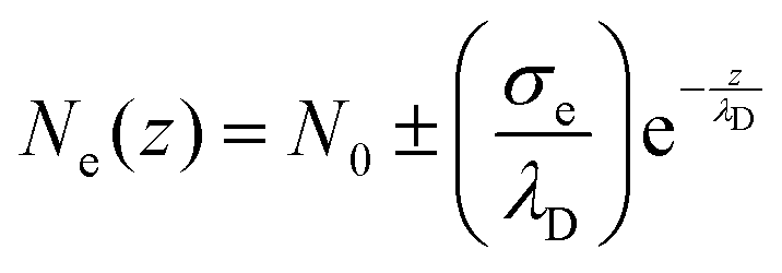
The effect of charge accumulation/depletion on the optical response was investigated by means of in operando spectroscopic ellipsometry (SE) versus an applied gate voltage VG in the range from −3 to +3 V. We exploited the extreme sensitivity of SE to very thin films in order to observe the voltage-induced tuning of the dielectric function of AZO in the ultrathin accumulation/depletion layer at the AZO/BTO interface. Then, we modelled the charge profile of the accumulation/depletion layer at the AZO/BTO interface and quantified the variations in the dielectric response of the TCO.To have an accurate estimation of the charge distribution within the interfacial injection/depletion layers, we therefore solved the full Poisson equation for an insulator–semiconductor interface:
 | (1) |
 | (2) |
The numerical solution of eqn (1) for our system for VG = 1, 2, and 3 V and the resulting charge profiles, as shown in Fig. 5, are strongly resembling exponential decays. Such exponential behavior can be approximated in ellipsometric simulations considering a well-defined value of the integrated charge and an exponential z-dependent charge profile, exploiting the Debye-length approximation.12 The overall accumulated/depleted charge can be retrieved by treating the system as a parallel-plate capacitor, where BTO acts as the dielectric, and the NSTO substrate and the AZO film are the two electrodes. The surface charge density σe can be written as follows:
 | (3) |
 | (4) |
 | ||
| Fig. 5 Charge profile for (a) accumulation and (b) depletion at the BTO/AZO interface as calculated from solution of the full Poisson equation. | ||
In addition to this, the optical model also considered the linear electro-optic effect in the BTO layer (Pockels effect).41 The effective refraction index neff due to the Pockels effect can be written as follows:
 | (5) |
Since the variations in the SE spectra due to the applied bias are not very large, they are best appreciated looking at the so-called difference spectra δΔ and δΨ, calculated by subtracting the unbiased data from the biased measurements. In Fig. 6, we report the experimental difference spectra δΔ and δΨ, recorded with an applied voltage VG = +0.2 V on AZO with respect to the NSTO back-electrode (markers). A marked signal has been detected even with a very low gate voltage already at room temperature, with δΔ displaying a pronounced peak reaching at around −0.5° of the shift between 1000 and 1200 nm. The δΨ signal is lower than δΔ, always below −0.05° of the shift, yet clearly observable. We restrict the following analysis on the VG = + 0.2 V case in order to avoid introducing any potential nonlinearity that might occur at higher electric fields.
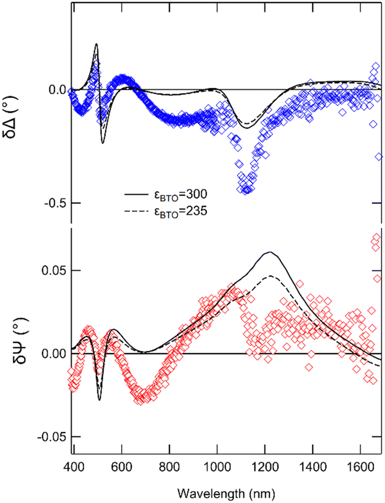 | ||
| Fig. 6 Measured and modelled differentials δΔ and δΨ of the ellipsometric angles with a +0.2 V bias applied. The solid (dashed) lines represent the calculated δ-spectra considering a value of εBTO = 235 (εBTO = 300) where both the Pockels effect in BTO and the charge accumulation at the AZO/BTO and NSTO/BTO interfaces are taken into account. | ||
The SE analysis of the biased sample essentially attempts to reproduce the experimental difference spectra δΔ and δΨ by computing the variations in Δ and Ψ taking place upon the application of the bias. We did not attempt to fit the difference spectra, but merely computed the expected variations based on the experimental data reported in the previous sections. The solid (dashed) lines in Fig. 6 represent the calculated δ-spectra considering a value of εBTO = 235 (εBTO = 300) where both the Pockels effect in BTO and the charge accumulation at the AZO/BTO and NSTO/BTO interfaces are taken into account. For the calculations, the Debye lengths were fixed at 1 nm for AZO and 9 nm for NSTO, and a variation of +0.003 of the ε1 of BTO was included. Despite the rather blunt approach, the model roughly captures the main features of the spectra, and especially for the δΔ spectra, where the wiggle around 500 nm and the peak between 1000 and 1200 are quite well reproduced. The δΨ differential has worse agreement especially in the NIR due to larger noise, while the visible region and its structures are reasonably fitted by the model, as for δΔ. In general, the contribution of charge accumulation is minor with respect to the Pockels effect, but still displays a non-negligible contribution, for instance helping the model to get close to the aforementioned peak in the δΔ signal.
The variation of +0.003 of the ε1 of the BTO, upon +0.2 V of applied voltage (roughly corresponding to 1.3 MV m−1), yields an effective r coefficient r ≃ 100 pm V−1 in very good agreement with literature values.42 Concerning the accumulated charge, we tested two values of εBTO, respectively, equal to εBTO = 235, i.e. the value obtained by the impedance measurements, and εBTO = 300, just slightly larger. The agreement with the experimental data for both values is quite similar.
In spite of the necessary assumptions and approximations due to the very complex system, we could however obtain an estimation of the actual charge profile at the AZO interface from the modelling. The charge profile extracted from the modeling is shown in Fig. 7a for a +0.2 V of applied voltage. A 6% increment with respect to the equilibrium optical carrier density n0 = 3.4 × 1020 cm−3 can be obtained already with a quite low gate voltage VG.
 | ||
| Fig. 7 (a) Charge profile in the AZO film as a function of the distance from the AZO/BTO interface as extracted from the modelling of the ellipsometric data. (b) Variations of the refractive index Δn as a function of wavelength and distance from the AZO/BTO interface. | ||
The variation of the refractive index Δn is calculated through the following formula derived from the Drude–Lorentz model15,43 and depends on both the wavelength λ and the distance from the interface. It reads
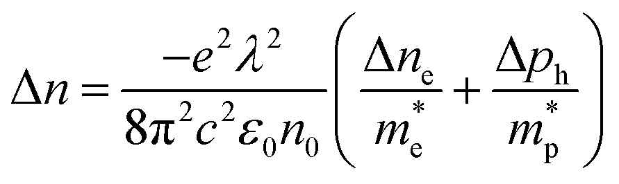 | (6) |
 and
and  represent their respective effective masses. In Fig. 7b, the variation of the AZO refraction index Δn at the interface with BTO due to the evaluated charge accumulation for +0.2 V of applied voltage is shown. At 1700 nm, a negative variation of more than 0.1 is reached with the charge unbalance at the AZO/BTO interface ΔNe = 0.2 × 1020 cm−3. In the absence of significant nonlinearities, this implies that at VG = +3 V (experimentally achievable without breakdowns in the system) Δn > 2 is achievable. In parallel, with VG = +3 V, a blue shift of the plasma frequency in AZO from λ = 1985 nm to around 1400 nm (at the interface) is expected.
Conclusions
Summarizing, we reported the realization, investigation and modeling of the FE-induced modulation of the optical response of micro-capacitors constituted by Al:ZnO/BaTiO3/Nb:SrTiO3 multilayer stacking. We characterized the electrical response of the capacitors by means of impedance analysis and the optical response of the system by means of in operando spectroscopic ellipsometry (SE). We detected a sizable bias-induced variation of the optical response that we ascribed to the combined effect of charge accumulation/depletion at the AZO/BTO and BTO/NSTO interfaces, accompanied by the voltage-induced Pockels effect in the BTO layer. The system could be operated at room temperature, and applied voltages as low as 0.2 V were sufficient to measure a variation of the optical response.We have modeled the bias-dependent variation of the optical response developing a complex optical model that accounts for exponentially graded charge injection and depletion layers and for the electro-optical effect in the BTO ferroelectric layer. Despite the complexity of the system and the variety of the physical effects concurring to its FE-induced variation of the optical response, we succeeded in modeling the optical response of each layer involved and in introducing the main bias-induced mechanisms that lie underneath the FE-induced variation of the refractive index in the infrared range up to a value of Δn of more than 0.1 at an applied bias of 0.2 V and by more than 2 at an applied bias of just 3 V.
This work therefore demonstrates the realization of a room temperature, low-voltage optical field-effect system and provides important clues to model and understand in detail the behavior and the working mechanisms of optically active systems, with relevant applications in the field of active photonics.
Author contributions
Methodology: R. M. M., M. M., P. T., A. d. B., S. B., and F. B.; formal analysis: R. M. M., M. M., M. S., and S. C.; investigation: R. M. M., M. M., M. S., S. C., and A. P.; data curation: R. M. M., M. M., S. C., A. P., and A. d. B.; writing – original draft preparation: R. M. M. and S. B.; writing – review and editing: R. M. M., M. M., M. S., S. C., S. D. A., A. P., M. C., P. T., A. d. B., S. B., and F. B.; supervision: S. D. A., M. C., P. T., S. B., and F. B.; funding acquisition: S. D. A., M. C., P. T., S. B., and F. B.; conceptualization: M. C., P. T., A. D. B., S. B., and F. B.Data availability
The data present in this article, including experimental curves and simulations used in figures, are available at Zenodo at https://doi.org/10.5281/zenodo.14833298.Conflicts of interest
There are no conflicts to declare.Acknowledgements
Authors acknowledge financial support under the National Recovery and Resilience Plan (NRRP), Mission 4, Component 2, Investment 1.1, Call for tender no. 104 PRIN 2022 published on 2.2.2022 by the Italian Ministry of University and Research (MUR), funded by the European Union – NextGenerationEU – Project Title ERACLITO – CUP B53D2300904006 and Call for tender no. 1409 PRIN PNRR 2022 published on 14.9.2022 by the Italian Ministry of University and Research (MUR), funded by the European Union – NextGenerationEU – Project Title ARCO – CUP B53D23027690001. This project has received further funding from the European Union's Horizon 2020 research and innovation program under the Marie Skłodowska-Curie grant agreement no. 799126.References
- T. Minami, Semicond. Sci. Technol., 2005, 20, S35–S44 CrossRef.
- K. Ellmer, Nat. Photonics, 2012, 6, 808–816 CrossRef.
- G. V. Naik, V. M. Shalaev and A. Boltasseva, Adv. Mater., 2013, 25, 3264–3294 CrossRef PubMed.
- R. A. Afre, N. Sharma and M. Sharon, Rev. Adv. Mater. Sci., 2018, 53, 79–89 Search PubMed.
- N. Kinsey, C. DeVault, J. Kim, M. Ferrera, V. M. Shalaev and A. Boltasseva, Optica, 2015, 2, 616–622 CrossRef.
- S. Vezzoli, V. Bruno, C. DeVault, T. Roger, V. Shalaev, A. Boltasseva, M. Ferrera, M. Clerici, A. Dubietis and D. Faccio, Phys. Rev. Lett., 2018, 120, 043902 CrossRef CAS PubMed.
- X. Niu, X. Hu, S. Chu and Q. Gong, Adv. Opt. Mater., 2018, 6, 1701292 CrossRef.
- A. K. Pradhan, R. M. Mundle, K. Santiago, J. R. Skuza, B. Xiao, K. D. Song, M. Bahoura, R. Cheaito and P. E. Hopkins, Sci. Rep., 2014, 4, 6415 CrossRef CAS.
- B. R. Bricchi, M. Sygletou, L. Ornago, G. Terraneo, F. Bisio, C. Mancarella, L. Stasi, F. Rusconi, E. Mogni, M. Ghidelli, P. Biagioni and A. Li Bassi, Mater. Adv., 2021, 2, 7064–7076 RSC.
- I. Valenti, S. Benedetti, A. Di Bona, V. Lollobrigida, A. Perucchi, P. Di Pietro, S. Lupi, S. Valeri and P. Torelli, J. Appl. Phys., 2015, 118, 165304 CrossRef.
- C. H. Zhai, R. J. Zhang, X. Chen, Y. X. Zheng, S. Y. Wang, J. Liu, N. Dai and L. Y. Chen, Nanoscale Res. Lett., 2016, 11, 407 CrossRef.
- M. Sygletou, S. Benedetti, A. di Bona, M. Canepa, F. Bisio and E. Bellingeri, ACS Appl. Mater. Interfaces, 2023, 3112 CrossRef CAS.
- C. H. Ahn, J. M. Triscone and J. Mannhart, Nature, 2003, 424, 1015–1018 CrossRef.
- K. Ueno, S. Nakamura, H. Shimotani, A. Ohtomo, N. Kimura, T. Nojima, H. Aoki, Y. Iwasa and M. Kawasaki, Nat. Mater., 2008, 7, 855–858 CrossRef.
- E. Feigenbaum, K. Diest and H. A. Atwater, Nano Lett., 2010, 10, 2111–2116 CrossRef PubMed.
- T. Cui, B. F. Bai and H. B. Sun, Adv. Funct. Mater., 2019, 29, 1806692 CrossRef.
- H. W. Zhao, Y. Wang, A. Capretti, L. Dal Negro and J. Klamkin, IEEE J. Sel. Top. Quantum Electron., 2015, 21, 3300207 Search PubMed.
- S. Zhu, G. Q. Lo and D. L. Kwong, Opt. Express, 2014, 22, 17930–17947 CrossRef.
- H. W. Lee, G. Papadakis, S. P. Burgos, K. Chander, A. Kriesch, R. Pala, U. Peschel and H. A. Atwater, Nano Lett., 2014, 14, 6463–6468 CrossRef PubMed.
- X. G. Liu, J. H. Kang, H. T. Yuan, J. Park, Y. Cui, H. Y. Hwang and M. L. Brongersma, ACS Photonics, 2018, 5, 1493–1498 CrossRef.
- D. Ghindani, A. R. Rashed, M. Habib and H. Caglayan, Adv. Opt. Mater., 2021, 9, 2100800 CrossRef.
- K. F. Shi and Z. L. Lu, Opt. Commun., 2016, 370, 22–28 CrossRef.
- Y. W. Huang, H. W. H. Lee, R. Sokhoyan, R. A. Pala, K. Thyagarajan, S. Han, D. P. Tsai and H. A. Atwater, Nano Lett., 2016, 16, 5319–5325 CrossRef PubMed.
- H. T. Yuan, H. Shimotani, A. Tsukazaki, A. Ohtomo, M. Kawasaki and Y. Iwasa, Adv. Funct. Mater., 2009, 19, 1046–1053 CrossRef.
- S. Saha, A. Dutta, C. DeVault, B. T. Diroll, R. D. Schaller, Z. Kudyshev, X. H. Xu, A. Kildishev, V. M. Shalaev and A. Boltasseva, Mater. Today, 2021, 43, 27–36 CrossRef.
- D. George, L. Li, D. Lowell, J. Ding, J. B. Cui, H. L. Zhang, U. Philipose and Y. K. Lin, Appl. Phys. Lett., 2017, 110, 071110 CrossRef.
- S. Abel, F. Eltes, J. Ortmann, A. Messner, P. Castera, T. Wagner, D. Urbonas, A. Rosa, A. Gutierrez, D. Tulli, P. Ma, B. Baeuerle, A. Josten, W. Heni, D. Caimi, L. Czornomaz, A. Demkov, J. Leuthold, P. Sanchis and J. Fompeyrine, Nat. Mater., 2019, 18, 42 CrossRef PubMed.
- T. Shimizu, D. Suwama, H. Taniguchi, T. Taniyama and M. Itoh, J. Phys.: Condens. Matter, 2013, 25, 132001 CrossRef PubMed.
- Y. Yoneda, T. Okabe, K. Sakaue, H. Terauchi, H. Kasatani and K. Deguchi, J. Appl. Phys., 1998, 83, 2458–2461 CrossRef.
- E. Bellingeri, D. Marré, I. Pallecchi, L. Pellegrino and A. S. Siri, Appl. Phys. Lett., 2005, 86, 012109 CrossRef.
- X. H. Wei, Y. R. Li, J. Zhu, W. Huang, Y. Zhang, W. B. Luo and H. Ji, Appl. Phys. Lett., 2007, 90, 151918 CrossRef.
- R. Magrin Maffei, A. di Bona, M. Sygletou, F. Bisio, S. D'Addato and S. Benedetti, Appl. Surf. Sci., 2023, 624, 157133 CrossRef.
- G. Vinai, F. Motti, A. Y. Petrov, V. Polewczyk, V. Bonanni, R. Edla, B. Gobaut, J. Fujii, F. Suran, D. Benedetti, F. Salvador, A. Fondacaro, G. Rossi, G. Panaccione, B. A. Davidson and P. Torelli, Rev. Sci. Instrum., 2020, 91, 085109 CrossRef.
- H. Fujiwara, Spectroscopic Ellipsometry: Principles and Applications, John Wiley & Sons, 2007 Search PubMed.
- M. Sygletou, S. Benedetti, A. di Bona, M. Canepa and F. Bisio, J. Phys. Chem. C, 2022, 126, 1881–1889 CrossRef.
- C. Herzinger and B. Johs, Guide to Using WVASE32, J. A. Woollam Company, 1996 Search PubMed.
- C. M. Herzinger and B. D. Johs, Dielectric function parametric model, and method of use, US Pat., 5796983, 1998, https://www.freepatentsonline.com/5796983.html Search PubMed.
- S. D. Guo and B. G. Liu, J. Appl. Phys., 2011, 110, 073525 CrossRef.
- S. Ohta, T. Nomura, H. Ohta and K. Koumoto, J. Appl. Phys., 2005, 97, 034106 CrossRef.
- A. Bikowski and K. Ellmer, J. Appl. Phys., 2013, 114, 063709 CrossRef.
- S. Misra, M. Kalaswad, D. Zhang and H. Y. Wang, Mater. Res. Lett., 2020, 8, 321–327 CrossRef.
- S. Abel, T. Stöferle, C. Marchiori, C. Rossel, M. Rossell, R. Erni, D. Caimi, M. Sousa, A. Chelnokov, B. Offrein and J. Fompeyrine, Nat. Commun., 2013, 4, 1671 CrossRef.
- G. T. Reed and C. E. J. Png, Mater. Today, 2005, 8, 40–50 CrossRef.
Footnote |
| † R. Magrin Maffei and M. Magnozzi contributed equally to this work. |
| This journal is © The Royal Society of Chemistry 2025 |