Graphdiyne for multilevel flexible organic resistive random access memory devices
Zhiwen
Jin
,
Yanhuan
Chen
,
Qing
Zhou
,
Peng
Mao
,
Huibiao
Liu
,
Jizheng
Wang
* and
Yuliang
Li
*
Beijing National Laboratory for Molecular Sciences, Key Laboratory of Organic Solids, Institute of Chemistry, Chinese Academy of Sciences, Beijing 100190, P. R. China. E-mail: jizheng@iccas.ac.cn; ylli@iccas.ac.cn
First published on 6th February 2017
Abstract
Graphdiyne (GD), a new carbon allotrope with a 2D structure comprising benzene rings and carbon–carbon triple bonds, is employed in fabricating resistive random access memory (RRAM) devices. On inserting a GD nanoparticle (NP) discontinuous layer and thermally depositing an Al–Al2O3 core–shell (Al–Al2O3) NP discontinuous layer in insulating polyimide (PI) films on a PET substrate, the designed flexible three-state memory device is realized (PET/Ag/PI/GD/PI/Al–Al2O3/PI/Al). GD NPs and Al–Al2O3 NPs function as two types of strong electron traps with different energy levels, resulting in two ON states. The OFF state and the two ON states possess long retention times of more than 104 s. Our results here demonstrate that GD could have great potential applications in future information storage technologies.
Conventional Si memory devices are currently approaching their scaling limits, and researchers are now enthusiastically developing new memory technologies to improve storage density and realize high-density integration.1–5 Multilevel memory devices can realize multi-state storage, and hence emerge as one of most attractive technologies.6–10 Moreover, resistive random access memory (RRAM) exploits the electric-field responsive resistive-switching of materials as an information write/erase principle for nonvolatile data storage;11–14 this technology is attracting more and more attention in the memory field, particularly organic-based ones due to their low cost, high flexibility, and 3-dimensional storage capability. Organic-based RRAM is expected to provide fast switching and high-density data storage for next-generation novel memory applications,15–18 and researchers have been trying various pathways to realize multi-states in organic-based RRAM systems.
Multilevel organic RRAM devices are generally fabricated based on a very fundamental architecture, namely a bottom electrode (BE)/active material/top electrode (TE) structure. In the early years, semiconductors were used as the active materials, and different conductive states were realized by controlling the filament formations under different bias sweeps.19,20 Later, novel materials were synthesized to realize multilevel storage capability by photoelectronic doping21,22 or electric-field-controllable doping.23,24 Then, composites consisting of organic materials and core–shell nanoparticles (NPs) were used; this structure showed that a negative differential resistance (NDR) and a different sweeping voltage will result in a multistate property in the NDR process by trapping/detrapping.25,26 Recently, researchers also fabricated multilevel devices through different traps induced by different dopants in the bulk materials.27,28 However, all the mentioned processes that are responsible for the multistate properties (including filament formation, doping and trapping) in bulk-composites films cannot be well-controlled by the applied bias, leading to unsatisfactory reproducibility and stability.29,30
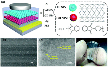
Forming different strong traps with different energy levels could be a feasible way to realize stable multilevel memory states.31 In this study, we utilized two different types of NPs to form two carrier traps in the designed organic RRAM shown in Fig. 1a. Specifically, discontinuous graphdiyne (GD) NP and Al–Al2O3 core–shell (Al–Al2O3) NP layers are inserted in the polyimide (PI) layer. From SEM images it is observed that both the GD layer (Fig. 1b) and Al–Al2O3 layer (Fig. 1c) are discontinuous and the two layers are well separated by the PI layers. The Ag bottom electrode (BE) and the Al top electrode (TE) serve as the anode and cathode, respectively. In such a structure (BE/PI/GD/PI/Al–Al2O3/PI/TE), the GD NPs and the Al–Al2O3 NPs are designed to act as two types of traps to generate multilevel memory states.
As a new carbon allotrope with a 2D structure comprising benzene rings and carbon–carbon triple bonds,32 GD shows an excellent performance in lithium-ion batteries,33 photodetectors34 and solar cells.35 Herein, GD NPs are designed to serve as a type of charge storage trap like graphene.36 The GD powder was synthesized according to a procedure reported in literature.32 The GD NP solution was prepared by dispersing the GD powder in chlorobenzene at a concentration of 1 mg ml−1 and was then ultrasonicated at 50 °C for more than a week. For the Al–Al2O3 core–shell NPs, the Al core is surrounded by a thin oxide shell of 1.5–2.0 nm.37Fig. 1d is a photograph of the fabricated flexible device on a polyethylene terephthalate (PET) substrate. All the devices in the manuscript were prepared by layer-by-layer processing. The PI films and GD NP film are solution processed (the solution concentration of PI in methyl-2-pyrrolidinone (NMP) is 10 mg ml−1 and GD in chlorobenzene is 1 mg ml−1) by spin-coating their solutions at 2000 rpm for 5 seconds and subsequently at 2000 rpm for 35 seconds. The prepared PI film was soft-baked on a hot plate at 120 °C for 10 min (to dry the solvent and cross-link the PI molecules). The Al–Al2O3 core–shell NP film was prepared by the thermal deposition of 4 nm-thick Al onto the beneath PI layer at a deposition rate of 0.05 nm s−1. Then, the Al NPs were exposed to air to form the Al–Al2O3 core–shell structure. The Ag and Al electrodes were thermally deposited with the help of a shadow mask at a deposition rate of 0.1 nm s−1, resulting in a 100 μm × 100 μm device area. The two electrodes are both 50 nm-thick.
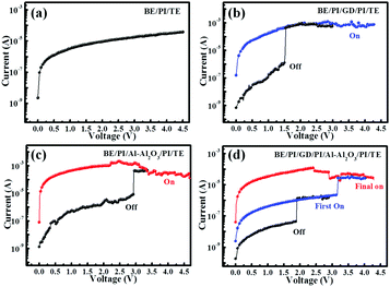
Fig. 2 shows the properties of four fabricated devices: the device without any NPs (BE/PI/TE), with only GD NPs (BE/PI/GD/PI/TE), with only Al–Al2O3 NPs (BE/PI/Al–Al2O3/PI/TE), and with both types of NPs (BE/PI/GD/PI/Al–Al2O3/PI/TE). It is seen that for the device without NPs (Fig. 2a), the I–V curve turned out to be smooth for both biasing directions, indicating that the device has no memory function. For the device with GD NPs (Fig. 2b) and the device with Al–Al2O3 NPs (Fig. 2c), they both present a bistable memory property during the bias sweep. The setting voltage is around 1.5 V for the GD based device, and is around 3 V for the Al–Al2O3 based device. This larger set voltage for the Al–Al2O3 based device is induced by the Al2O3 barrier shell, which requires a larger applied bias to trap electrons from PI into the Al core.38
For the device with both NPs (Fig. 2d), it is turned to the first ON state from its initial pristine OFF state at a bias around 1.7 V, which can be maintained until the bias is increased to 3.1 V, the point at which the device is switched to its final ON state. To conclude, the device possesses three states: the pristine OFF state before 1.7 V, the first ON state between 1.7 V and 2.1 V, and the final ON state after 3.1 V. The device cannot be turned OFF from its ON states by applying a negative bias, making it a write-once-read-many type (WORM) memory device. For the three states, the conductivity differs largely, which leads to large current ratios between them (between the OFF state and the first ON state or between the first ON state and the final ON state). Based on the properties of the four devices, we can reliably conclude that the memory properties are indeed from the GD NPs and Al–Al2O3 NPs, with the lower-bias one originating from the GD NPs and the higher-bias one originating from the Al–Al2O3 NPs.
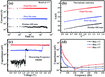
Afterwards, we measured the electric maintaining ability for every state: we first applied different biases to set the device to the three states, and then fixed the bias at 1 V to test the current fluctuation with time. From the results shown in Fig. 3a, it is seen that the current fluctuates very little in a long duration of 104 s. This indicates that the device has a strong retention ability and the three states are all very stable.
The memory mechanism in our device should be originating from carrier tunneling and trapping effects, similar to that reported.37,38 During the bias scan, carriers are first injected into the GD NPs at a bias around 1.7 V, and then into the Al–Al2O3 NPs at a bias around 3.1 V, and are sequentially trapped in the two NP layers. Therefore, there would be different trapped charges in the device at different states. The I–V curves were fitted to investigate the carrier transport mechanism and the tunneling mechanism in the RRAM device using the thermionic emission conduction (TEC) model:39,40
The capacitance versus voltage is shown in Fig. 3c (including the voltage sweeping mode and the frequency sweeping mode). It is seen that with varying the bias voltage, the capacitance first increases from its initial value to a relatively large value at a bias around 2 V and then to its largest value at a bias around 4 V. The three capacitance values should correspond to the pristine OFF state, the first ON state and the final ON state. The three states are also evident in the frequency sweeping mode (Fig. 3d), when biased under different voltages. Combining the fitting results and the capacitance experiments, we believe that electrons are injected from the Ag electrode into the NPs via the TE process and are then trapped in the NPs.
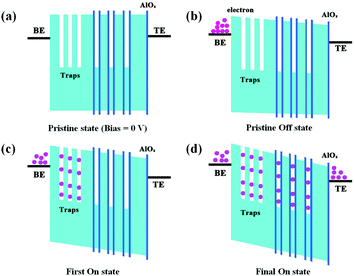
The operation mechanism of the multilevel switching is presented in Fig. 4. Fig. 4a shows the energy level of the pristine state at 0 V without any electrons trapped. During the voltage sweep between 0 V to 1.7 V (Fig. 4b), PI prevents electrons from being injected into the electron traps of the GD NPs and the Al–Al2O3 NPs. As a result, the pristine state is stabilized and the device is kept at a high resistance state (HRS). During the first sweep from 0 V to 3 V (Fig. 4c), when the voltage is large enough to overcome the potential barrier formed between the PI and the Ag electrode, electrons are first trapped in the GD NPs, and the device is set to the first ON state. Then, the device is transited from the HRS to an intermediate resistance state (IRS). Owing to the higher Al2O3 tunneling barrier shells, electrons cannot be injected into the Al cores. During the second sweep from 0 V to 4 V (Fig. 4d), electrons are injected into the Al cores, and the device is set to its second ON state, the low resistance state (LRS), where it remains.
 | ||
| Fig. 4 Switching mechanism of the fabricated multi-state device: (a) pristine state. (b) Pristine OFF state. (c) First ON state. (d) Final ON state. | ||
Conclusions
In summary, we fabricated three-state organic RRAM with high reproducibility and stability by employing the novel carbon material GD and metal/oxide core–shell NPs. The GD NPs produce one ON state and the metal/oxide core–shell NPs produce another ON state. The retention times of the OFF state and the two ON states are all over 104 s. On careful analysis based on the I–V curve fitting and the C–V measurements, we conclude that a carrier tunneling process through the insulator layers and a carrier trapping effect in the two NP layers are responsible for the multilevel memory observations. This study demonstrates that the novel carbon material GD could have great applications in future information storage technologies.The authors acknowledge the financial support by 973 Program (Grant No. 2016YFA0200104, 2014CB643600 and 2014CB643503), National Natural Science Foundation of China (61405208) and the Strategic Priority Research Program of the Chinese Academy of Sciences (Grant No. XDB12030200).
Notes and references
- X. Zhang, Y. He, R. Li, H. Dong and W. Hu, Adv. Mater., 2016, 28, 3755–3760 CrossRef CAS PubMed.
- L. Liang, et al. , J. Am. Chem. Soc., 2015, 137, 3102–3108 CrossRef CAS PubMed.
- R. H. Kim, et al. , Nat. Commun., 2014, 5, 3583 Search PubMed.
- M. J. Lee, et al. , Nat. Mater., 2011, 10, 625–630 CrossRef CAS PubMed.
- Z. Jin, G. Liu and J. Wang, J. Mater. Chem. C, 2013, 1, 3282–3286 RSC.
- Q. Zhang, et al. , Chem. – Asian J., 2016, 11, 1624–1630 CrossRef CAS PubMed.
- S. K. Hwang, I. Bae, R. H. Kim and C. Park, Adv. Mater., 2012, 24, 5910–5914 CrossRef CAS PubMed.
- G. Yang, H.-Y. Chen, L. Ma, Y. Shao and Y. Yang, Appl. Phys. Lett., 2009, 95, 203506 CrossRef.
- G. Jiang, Y. Song, X. Guo, D. Zhang and D. Zhu, Adv. Mater., 2008, 20, 2888–2898 CrossRef CAS.
- M. Rozenberg, I. Inoue and M. Sánchez, Phys. Rev. Lett., 2004, 92, 178302 CrossRef CAS PubMed.
- Y. Li, et al. , Adv. Funct. Mater., 2015, 25, 4246–4254 CrossRef CAS.
- Y. Ji, S. Lee, B. Cho, S. Song and T. Lee, ACS Nano, 2011, 5, 5995–6000 CrossRef CAS PubMed.
- T.-W. Kim, et al. , Adv. Mater., 2012, 24, 828–833 CrossRef CAS PubMed.
- R. Waser and M. Aono, Nat. Mater., 2007, 6, 833–840 CrossRef CAS PubMed.
- G. Liu, Z. Jin, Z.-G. Zhang and J. Wang, Appl. Phys. Lett., 2014, 104, 023303 CrossRef.
- Y.-C. Lai, et al. , NPG Asia Mater., 2014, 6, e87 CrossRef CAS.
- Y. Ji, et al. , Nat. Commun., 2013, 4, 2707 Search PubMed.
- Q. D. Ling, et al. , J. Am. Chem. Soc., 2006, 128, 8732–8733 CrossRef CAS PubMed.
- M. Lauters, B. McCarthy, D. Sarid and G. Jabbour, Appl. Phys. Lett., 2006, 89, 013507 CrossRef.
- M. Cölle, M. Büchel and D. M. de Leeuw, Org. Electron., 2006, 7, 305–312 CrossRef.
- H. Tan, et al. , Adv. Mater., 2015, 27, 2797–2803 CrossRef CAS PubMed.
- C. Ye, et al. , J. Am. Chem. Soc., 2012, 134, 20053–20059 CrossRef CAS PubMed.
- Q.-F. Gu, et al. , Adv. Mater., 2015, 27, 5968–5973 CrossRef CAS PubMed.
- B. Hu, et al. , J. Am. Chem. Soc., 2012, 134, 17408–17411 CrossRef CAS PubMed.
- G. Casula, et al. , Org. Electron., 2015, 18, 17–23 CrossRef CAS.
- J.-G. Park, et al. , Nano Lett., 2009, 9, 1713–1719 CrossRef CAS PubMed.
- S. K. Hwang, et al. , Nano Lett., 2012, 12, 2217–2221 CrossRef CAS PubMed.
- Y. Sun, J. Lu, C. Ai, D. Wen and X. Bai, Org. Electron., 2016, 32, 7–14 CrossRef CAS.
- B. Cho, S. Song, Y. Ji, T.-W. Kim and T. Lee, Adv. Funct. Mater., 2011, 21, 2806–2829 CrossRef CAS.
- Q.-D. Ling, et al. , Prog. Polym. Sci., 2008, 33, 917–978 CrossRef CAS.
- J. Ouyang, C.-W. Chu, C. R. Szmanda, L. Ma and Y. Yang, Nat. Mater., 2004, 3, 918–922 CrossRef CAS PubMed.
- G. Li, et al. , Chem. Commun., 2010, 46, 3256–3258 RSC.
- C. Huang, et al. , Nano Energy, 2015, 11, 481–489 CrossRef CAS.
- Z. Jin, et al. , Adv. Mater., 2016, 28, 3697–3702 CrossRef CAS PubMed.
- Z. Jin, et al. , Adv. Funct. Mater., 2016, 26, 5284–5289 CrossRef CAS.
- Y. Ji, et al. , Nanotechnology, 2012, 23, 105202 CrossRef PubMed.
- V. S. Reddy, S. Karak and A. Dhar, Appl. Phys. Lett., 2009, 94, 173304 CrossRef.
- L. Ma, S. Pyo, J. Ouyang, Q. Xu and Y. Yang, Appl. Phys. Lett., 2003, 82, 1419 CrossRef CAS.
- M. A. Lampert and P. Mark, Current injection in solids, Academic Press, New York, 1970 Search PubMed.
- Z. Jin, G. Liu and J. Wang, AIP Adv., 2013, 3, 052113 CrossRef.
| This journal is © the Partner Organisations 2017 |


