
Conduction band position tuning and Ga-doping in (Cd,Zn)S alloy thin films†
Lauryn L.
Baranowski
 ab,
Steven
Christensen
a,
Adam W.
Welch
ab,
Stephan
Lany
a,
Matthew
Young
a,
Eric S.
Toberer
b and
Andriy
Zakutayev
*a
ab,
Steven
Christensen
a,
Adam W.
Welch
ab,
Stephan
Lany
a,
Matthew
Young
a,
Eric S.
Toberer
b and
Andriy
Zakutayev
*a
aNational Renewable Energy Laboratory, 15013 Denver West Parkway, Golden, CO 80401, USA. E-mail: andriy.zakutayev@nrel.gov
bColorado School of Mines, 1500 Illinois St., Golden, CO 80401, USA
First published on 13th February 2017
Abstract
In recent years, the number of novel photovoltaic absorber materials under exploration has rapidly increased. However, to reap the most benefit from these new absorbers, alternative device structures and components must also be considered. In particular, the choice of a heterojunction partner, or contact layer, is critical to device optimization. In this work, we explore alternative n-type contact layer candidates that could be widely applicable to a variety of new absorbers. We use theory to calculate the band edge tuning provided by a variety of II–VI alloy systems, and select the (Cd,Zn)S system as one that affords a wide range of conduction band tuning. The synthesis of (Cd,Zn)S alloys is explored using atomic layer deposition, which afforded precise compositional control and produced crystalline thin films. The predicted tuning of the band gap and conduction band minimum is confirmed through X-ray photoelectron spectroscopy and optical absorption measurements. In addition, we investigated Ga-doping in Cd0.6Zn0.4S films to decrease their series resistance when used as contact layers in photovoltaic devices. This study provides a framework for exploring and optimizing alternative contact layer materials, which will prove critical to the success of new PV absorbers.
1 Introduction
The need for scalable, low cost, and non-toxic photovoltaic materials is a pressing challenge in today's energy landscape. In recent years, a variety of earth abundant photovoltaic absorbers have been investigated, including Cu2ZnSn(S,Se)4 (CZTS), Cu2SnS3, SnS, CuSb(S,Se)2, and Sb2Se3.1–6 With the increased exploration of new absorber materials also comes the need to revisit material choices for the other components of the photovoltaic device stack. In particular, the choice of heterojunction contact, or buffer layer, is critical to overall device performance and needs to be optimized for each new absorber.The choice of buffer layer in a photovoltaic device greatly influences the charge separation at the absorber/buffer interface, and thus the ultimate device performance. Any successful buffer layer must satisfy several requirements,7 including
(1) sufficiently wide bandgap to reduce parasitic absorption,
(2) suitable conduction band offset (CBO) at the absorber/buffer interface for optimal charge collection,
(3) low defect density at the absorber/buffer interface,
(4) sufficiently high doping with a Fermi level position above that of the absorber.
It is generally accepted that the desired CBO at the absorber/buffer interface is a small “spike” type offset, in which the conduction band minimum of the buffer layer is 0–0.3 eV higher than that of the absorber layer, as shown on the left side of Fig. 1.3 A spike significantly larger than 0.3 eV creates a barrier that impedes the collection of photo-generated carriers. Conversely, if the CBO is a “cliff” type offset (conduction band minimum of the buffer is lower than that of the absorber), the device suffers from increased interface recombination (see Fig. 1).
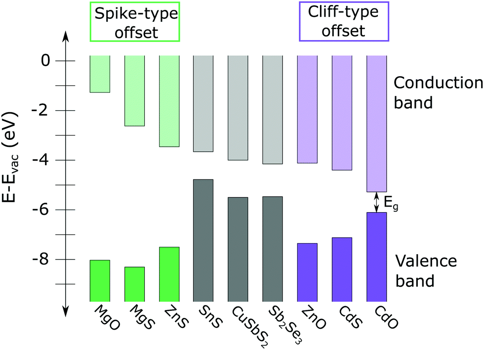 | ||
| Fig. 1 Calculated conduction band minima (CMB) and valence band maxima (VBM) of several high conduction band thin film absorbers, including SnS, CuSbS2, and Sb2Se3 (from ref. 8, 4 and 9, respectively) and a variety of n-type II–IV buffer layers (from ref. 10). A large spike-type offset (compounds on the left side of the figure, shown in green) impedes collection of photo-generated carriers. Significant cliff-type offsets (compounds on the right side of figure, in purple) can result in increased interface recombination. In general, a 0–0.3 eV spike is considered optimal for photovoltaic device performance. | ||
CdS is by far the most widely used buffer layer for thin film photovoltaics such as Cu(In,Ga)Se2 (CIGS) and CZTS. However, many alternatives to CdS have been considered either to address the issue of Cd toxicity, or to optimize the CBO for novel absorber layers. Many alternative buffer layers are II–VI compounds or alloys, including ZnS, ZnSe, Zn(O,S), (Zn,Mg)O, (Zn,Sn)O, and (Cd,Zn)S.11–15 Most often, chemical bath deposition (CBD) is used to deposit the buffer layers on the as-grown absorbers, because it is believed that a built-in etching effect from the basic chemical bath results in low interfacial recombination. However, CBD processes can result in oxide or hydroxide impurities in sulfide films.16 Other techniques, such as atomic layer deposition (ALD) and sputter deposition offer better compositional control, but may result in less desirable interfacial properties (such as higher defect densities) than CBD.13,17 The material properties of these II–VI alloys have also been investigated via both experiment18–24 and theory,25,26 with a particular focus on nanostructures and epitaxial thin films.
In this work, we use theory and experiment to identify potential alternative buffer layer materials for thin film absorbers in which the conduction band position differs from that of the traditional CdS contact. First principles theory was used to screen a variety of II–VI alloy systems as buffer layer candidates. Experimentally, we find that we can grow crystalline (Cd,Zn)S alloys with precise compositional control using ALD. Furthermore, these alloys provide a wide range of conduction band edge tunability, which is evidenced by X-ray photoelectron spectroscopy (XPS) data. An interesting new class of absorbers to which these alternative contact layers could be applied are the CuSbCh2 (Ch = S, Se) materials. Recent theoretical work suggests that the efficiencies of these devices (≤3%) could be improved through optimization of the conduction band offset between the p-type CuSbCh2 absorber and the n-type buffer layer.4,5,27 As a proof of concept, we integrate the Ga-doped Cd0.6Zn0.4S buffer into a photovoltaic device with a CuSbS2 absorber layer, and see a significant enhancement in open circuit voltage (VOC) compared to a CBD CdS buffer layer. Overall, we find that Ga-doped (Cd,Zn)S buffers represent a possible alternative to the traditional CdS buffers, although further optimization of the material is necessary for high efficiency devices.
2 Methods
2.1 (Cd,Zn)S thin film growth
The (Cd,Zn)S films were grown using atomic layer deposition (ALD) in a Beneq TFS 200 reactor. The precursors for ALD growth were dimethyl cadmium (DMCd, Strem), diethyl zinc (DEZ, Aldrich), tris(dimethylamino)gallium (TDMAGa, Gelest), and H2S (15% H2S/N2 mixture, Matheson). The DMCd and DEZ were held at 20 °C, whereas the TDMAGa precursor was heated to 118 °C. The reactor optimized precursor sequence timing was the following: DEZ and DMCd dose/purge = 200 ms/2 s; H2S pulse/purge = 200 ms/3 s; TDMAGa pulse/purge = 1.5 s/5 s. Ultra-high purity nitrogen (99.999%) was used as the carrier and purge gas at a flow rate of 550 sccm and the reactor pressure was operated at ∼1 Torr. All films were deposited with a substrate temperature of 150 °C. Si, FTO-coated glass, and anodized Al2O3 witnesses were included with each deposition.Different compositions of (Cd,Zn)S were obtained by varying the (DEZ/H2S) to (DMCd/H2S) ratio. For example, an xALD = 0.1 refers to the base composition of 9 ALD cycles of DMCd/H2S to 1 ALD cycle of DEZ/H2S; xALD is the fraction of DEZ/H2S cycles. Films were grown by multiples of the base composition sequences to target desired thicknesses (see Table S1 in the ESI†).
We explored the use of several group III elements for doping of our Cd1−xZnxS films. Initial aluminum doping efforts were conducted using a trimethyl aluminum precursor. However, we observed no Al incorporation when using our established growth temperature for Cd1−xZnxS. Gallium doping was achieved at our 150 °C growth temperature by introducing TDMAGa/H2S cycles in between sequences of the base composition. From preliminary experiments with TDMAGa, we found that the growth rate was significantly slower than for the DMCd or DEZ. Thus, for the purposes of integrating the Ga into the (Cd,Zn)S films, we considered 5 cycles of TDMAGa to be equivalent to 1 cycle of DMCd/DEZ. The Ga-doped samples were synthesized with an xALD value of 0.5 (1 cycle of DMCd:1 cycle of DEZ). Three levels of Ga doping were investigated at approximate ratios of 1![[thin space (1/6-em)]](https://www.rsc.org/images/entities/char_2009.gif) :10, 1:20, and 1:30. For all samples, the base sequence was repeated multiple times to achieve the desired film thickness.
:10, 1:20, and 1:30. For all samples, the base sequence was repeated multiple times to achieve the desired film thickness.
The CdS chemical bath deposited (CBD) buffer layer (used as a control sample) was synthesized by immersing the sample in a solution of 100 mL DI H2O, 12.5 mL of ammonium hydroxide (NH4OH, 28–30%), 10 mL of cadmium sulfate (CdSO4, 0.015 M), and 5 mL of thiourea (NH2CSNH2, 1.5 M). The chemicals were combined in a water-jacketed vessel at 65 °C and the bath was continuously stirred during deposition. The sample was removed after 12 minutes and rinsed with DI water. Further details can be found in ref. 28.
2.2 Thin film characterization
The composition of the (Cd,Zn)S thin films was determined by energy dispersive X-ray spectroscopy (EDX) using NORAN System SIX software, version 1.8, in an FEI Quanta600 scanning electron microscope (SEM). This analysis was performed on the Si witness samples. The software contained internal calibration factors that were tested using Zn-free CdS and Cd-free ZnS as references. X-ray diffraction patterns were collected from the anodized Al2O3 witnesses using a θ–2θ geometry with Cu Kα radiation and a proportional 2D detector (Bruker D8 Discover with General Area Detector Diffraction System software). Film thickness was measured using ellipsometry on the Si witnesses. UV/Vis reflectance and transmittance were measured from 300–1200 nm on FTO witnesses using a fiber-optics-based spectrometer with deuterium and tungsten/halogen light sources and Si and InGaAs detector arrays. The absorption coefficient was calculated from the measured reflectance (R) and transmittance (T) spectra, and the measured film thickness (d) from ellipsometry, using the relationship α = −ln[T/(1 − R)]/d. The band gaps were estimated using a Tauc plot for a direct band gap semiconductor. The electrical resistivity of the buffers was determined by evaporating Ag contact pads onto the front of the film and measuring the resistance between two probes placed on (1) the contact pad and (2) the bare surface of the film about 5 mm away from the contact pad. The X-ray photoelectron spectroscopy (XPS) measurements were performed on a Kratos AXIS Nova instrument using Al Kα X-rays and Vision software, version 2.2.10. Core level data were obtained with a pass energy of 20 eV. Samples were exposed to air before being loaded into the instrument. Valence band data were taken with a pass energy of 5 eV. As with the EDX compositional data, the internal calibration factors of the Vision software were tested using Zn-free CdS and Cd-free ZnS samples.2.3 Photovoltaic device fabrication and characterization
The CuSbS2 absorber layers were grown on Mo-coated soda lime glass substrates. RF magnetron sputtering was performed using one Cu2S target and two Sb2S3 targets. The RF power on each target was the same, resulting in an excess flux of Sb2S3. The substrate was heated to 400 °C, which resulted in stoichiometric CuSbS2, due to self-regulated growth.29 Substrates were rotated during growth, which resulted in a uniform layer thickness; the layer thickness was controlled by varying the deposition time. More details of the absorber layer growth and characterization can be found in ref. 4 and 29. After the initial sputter deposition, CuSbS2 films were annealed in an Sb2S3 atmosphere at 430 °C for 10 hours. Details of the annealing process can be found in ref. 30. Just prior to the buffer layer deposition, the samples were etched in 0.1 M KOH for 30 minutes to preferentially remove the Sb-rich oxide layers from the CuSbS2 surface.31After the CuSbS2 absorber is deposited on 50 mm × 50 mm substrate, the resulting sample is cleaved into 8 pieces (12.5 mm × 25 mm). Five devices are fabricated on each piece. It is important to note that for each sample set of devices with varying buffer layer composition, all devices in that sample set are made with the same CuSbS2 absorber. For example, in Fig. S3 (ESI†), all devices shown are from one CuSbS2 sample, with different buffer layers deposited on parts of that sample. This is done because factors such target and heater aging produced variations between CuSbS2 samples. To be able to confidently compare the effects of different buffer layers, it was critical to use the same underlying absorber.
After buffer layer deposition, the devices were finished by depositing layers of intrinsic ZnO and conductive Al:ZnO by RF sputtering, and Al metal contacts using e-beam evaporation. Devices were isolated using photolithography. A schematic of the device stack can be seen in ref. 4. Device performance was measured using a custom, spatially resolved, current–voltage characterization instrument with simulated AM1.5G illumination and a water cooled stage (25 °C).
2.4 First principles calculations
The ionization potentials (IP) and electron affinities (EA) have been calculated by a combination of density functional theory (DFT) and GW quasiparticle energy calculations. The current results extend upon data published in ref. 10, in which the IP and EA were determined for the binary II–VI compounds. Employing the projector augmented wave (PAW) implementation for DFT and GW calculations in the VASP code,32,33 we determined the potential step at the surface, and used the GW quasiparticle energies to determine the positions of the VBM and CBM with respect to the vacuum level. For the II–VI alloys, we used the (110) surface of the zinc blende structure, and the special quasi-random structures (SQS) of ref. 34 for the alloy compositions of 25, 50, and 75%. For CuSbS2, which has an orthorhombic structure, we calculated the IP/EA for the (001), (010) and (100) surfaces, which have surface energies of 12, 14, and 23 meV A−2, respectively. The GW calculations follow the same computational scheme used for the larger data set of electronic structure calculations for semiconductors and insulators, including transition metal compounds,35 which is accessible at http://materials.nrel.gov.3 Results and discussion
3.1 Theoretical evaluation of band edge tuning in II–VI alloy systems
First principles theory was used to screen a variety of II–VI alloy systems for their suitability as buffer layers for CuSbS2 absorbers, including (Zn,Mg)O, (Zn,Cd)O, (Cd,Zn)S, (Cd,Mg)S, Zn(O,S), and Cd(O,S). The Zn(O,S) system has been considered previously in ref. 25, which also predicted the valence band bowing effect observed here. The changes in valence and conduction band edges were calculated relative to vacuum, and compared to the calculated valence band maximum (VBM) and conduction band minimum (CBM) positions for CuSbS2. Most important was to select an alloy system that afforded a wide range of tunability in the CBM position. This characteristic allows the buffer to be integrated with various absorber layers, and for experimental optimization of the CBO through compositional tuning of the buffer layer. For our proof of concept device integration, we targeted the desired flat or small spike type CBO with our CuSbS2 absorber.With the above considerations in mind, we determined that the most promising candidates were the Cd1−xMgxS and Cd1−xZnxS alloy systems. The calculated VBM and CBM positions as a function of composition can be seen in Fig. 2 (corresponding figures for the other alloy systems can be found in Fig. S1, ESI†). We also include the conduction band minimum of CuSbS2 calculated for several possible surfaces.4 The Cd1−xMgxS compound is particularly interesting, because the CBM is increased significantly by the addition of only a small amount of Mg. However, we found that we were not able to synthesize this compound via atomic layer deposition (ALD) because of the large differences in required reactor temperature for growth from the Cd and Mg precursors, as well as the poor reactivity between the Mg precursor and the H2S gas. This system remains of interest as an alternative buffer layer candidate, but only one successful synthesis has been reported in the literature via CBD.36 We thus turned our attention to the Cd1−xZnxS system, which has been investigated previously for use with CIGS and CdTe absorbers.15,37,38
 | ||
| Fig. 2 Calculated valence band maxima and conduction band minima for several n-type contact layer candidates. (a) We identified the Cd1−xMgxS and Cd1−xZnxS cation alloy systems as promising for use with a CuSbS2 absorber, due to their wide range of conduction band minima tunability. (b) In contrast, the anion alloy systems, including the commonly used ZnO1−xSx, provide a much smaller range of CBM tuning. | ||
It is of note that we eliminated the Zn(O,S) alloys from our list of buffer layer candidates. Zn(O,S) buffers have been used in many thin film photovoltaic devices, with both traditional thin film absorbers (CIGS) and new materials (SnS).3,11 However, our calculations suggest that the range of CBM tunability is quite narrow over the entire ZnO–ZnS alloy range, as shown in Fig. 2b. Our results are qualitatively similar to the results of ref. 25, which first predicted the strong valence band bowing and minimal conduction band tuning observed here. Thus, while Zn(O,S) buffers may provide optimal CBOs when Cd-free contact layers are desired for use with CIGS and CZTS absorbers, they do not offer the tunability or widespread applicability that we are targeting in this study.
3.2 Growth and characterization of the Cd1−xZnxS alloy system
We varied the composition of the Cd1−xZnxS films with ALD pulse ratios designed to give x values of 0, 0.1, 0.5, 0.9, and 1. When the resulting films were measured using energy dispersive X-ray spectroscopy (EDX), we found that the intermediate compositions were slightly Zn deficient, which is in agreement with previous literature.39 The ALD pulse ratios of x = 0.1, 0.5, and 0.9 resulted in Cd1−xZnxS film compositions of x = 0.10, 0.39, and 0.86, respectively, as shown in Fig. 3. By analyzing core levels peaks from the X-ray photoelectron spectroscopy (XPS), the film compositions appeared to be slightly Zn rich. However, this could be due to preferential removal of the Zn during the XPS sputter depth profiling. Thus, in the following sections, we will use the stoichiometries as determined by EDX to refer to each sample. | ||
| Fig. 3 Comparison of the initial Cd/Zn ratio (per the ALD precursor pulse ratio) and the final film composition (determined via energy dispersive X-ray spectroscopy and X-ray photoelectron spectroscopy). We successfully controlled the Cd/Zn ratio in our resultant films by adjusting the precursor pulse ratios during ALD growth. EDX data suggested that the intermediate compositions were slightly Zn deficient, while XPS data showed slightly Zn rich compositions. | ||
We note that this level of compositional control and film homogeneity for the ALD films is much better than that afforded by CBD of the Cd1−xZnxS alloy system. Although many studies claim to use CBD Cd1−xZnxS contact layers, most rely on the starting ratio of Cd/Zn in the chemical bath, rather than measuring the actual composition of the resultant film. Only a few studies have used techniques such as inductively coupled plasma analysis or XPS to prove that intermediate compositions were actually synthesized.15,40 In our own work, we attempted to recreate the experiments detailed in ref. 15, but these resulted in either pure CdS or ZnS. Thus, our thin films synthesized via ALD allow for a much more systematic study of property changes with composition.
We next investigated the crystal structure of the Cd1−xZnxS films using X-ray diffraction (XRD). The XRD patterns, along with reference patterns for wurtzite CdS and ZnS, are shown in Fig. 4. All of the peaks in the CdS diffraction pattern can be ascribed to the hexagonal wurtzite crystal structure (JCPDS no. 41-1049). As Zn is alloyed into the structure, we see a peak shift to higher 2θ values, as would be expected for a decrease in lattice parameter (see Fig. S2 in the ESI† for peak shift data). The peak shifts, rather than peak splitting, provide evidence that we are achieving a true Cd1−xZnxS alloy without phase separation. In the majority Zn-samples (Cd0.14Zn0.86S and ZnS), the films remain in the wurtzite structure (JCPDS no. 36-1450), but with notable changes in relative peak intensities. However, because the XRD patterns were acquired from the porous Al2O3 witnesses it is difficult to infer much from this trend, as the preferential orientations implied by relative peak intensity shifts may be different on the Si or FTO substrates.
 | ||
| Fig. 4 All Cd1−xZnxS films displayed the hexagonal wurtzite structure. Peak shifts to higher 2θ values with the addition of more Zn indicate the expected decrease in lattice parameter, and demonstrate that true alloying is occurring, rather than phase separation. | ||
Further evidence for alloying is found in the optical absorption spectra, as shown in Fig. 5a. As the Zn content of the films is increased, we observe the expected shift of the absorption edge to higher energies. All films show the steep absorption onset corresponding to a direct optical transition. We used the Tauc method for direct allowed transitions to estimate the band gap of each sample; these values ranged from 2.4 eV for the CdS to 3.5 eV for the ZnS, shown in Fig. 5b.41 The CdS optical absorption edge matches well with the reference value of 2.4 eV.11 Our measured band gap for ZnS is lower than expected, which is likely due to optical absorption by the substrate.
 | ||
| Fig. 5 (a) The optical absorption spectra show steep absorption onsets characteristic of direct band gap materials. (b) Estimated band gaps (via the Tauc method) show the expected shift to higher energies with increasing Zn content. Reference values for CdS and ZnS from ref. 11. | ||
3.3 Band edge tuning in the Cd1−xZnxS alloy system
To quantify the band edge tuning as a function of Zn content, we performed valence band XPS measurements on CuSbS2/Cd1−xZnxS layered samples. After the surface oxide was removed by an initial sputtering (T1), the spectra acquired at sputter time T2 (Fig. 6a) were representative of the (Cd,Zn)S layer. With further sputtering (sputter time T3), the spectra from all samples were the same, indicating that the (Cd,Zn)S layers had been sputtered through. These spectra at T3 thus represent the identical CuSbS2 absorber layers of each sample. | ||
| Fig. 6 (a) XPS spectra at time T2 were acquired within the Cd1−xZnxS contact layer and show different binding energy edges, indicating tuning of the valence band edge. The identical spectra at time T3 correspond to the underlying CuSbS2 layer. (b) From the XPS and optical absorption data, we estimated the positions of the VBM and CBM of our Cd1−xZnxS films relative to CuSbS2. From this, we are able to predict that a Cd0.4Zn0.6S contact layer would provide optimal conduction band alignment with CuSbS2. | ||
Linear fits of the spectra at time T2 were used to estimate the position of the valence band for each Cd1−xZnxS layer composition. Then, the band gap (as determined from the absorption data in Fig. 5b) was added to the valence band position to calculate the conduction band minimum. These are shown in Fig. 6b relative to the CuSbS2 band edges. As expected from our theoretical calculations (Fig. 2), we see an increase in the conduction band edge with increased Zn content. When we consider the desired conduction band offset between the CuSbS2 absorber and the Cd1−xZnxS layer, we can conclude that the optimal x value is approximately 0.6.
We observed highly resistive behavior for the higher Zn content films (Cd0.61Zn0.39S and Cd0.14Zn0.86S, see Fig. S3, ESI†). We measured the resistance of the films between a metal contact sputtered on the surface of the film and a point on the film about 5 mm away, and found that the buffers with the desired Zn content (between x = 0.39–0.86) had extremely high resistances on the order of 10–100 MΩ; this effect has previously been observed in other studies.17
3.4 Ga-Doping of Cd0.6Zn0.4S
To address the issue of high resistivity in the higher Zn content Cd1−xZnxS alloys, we investigated doping of the alloy films with a group III element. Successful doping in Cd1−xZnxS buffers has previously only been reported with a Cu dopant.42 We initially considered Al for the dopant element, but the trimethyl aluminum ALD precursor did not react with the H2S gas at our 150 °C deposition temperature. In contrast, the tris(dimethylamino)gallium precursor proved easier to integrate into our existing ALD growth processes for the Cd1−xZnxS films. Our XPS data in Fig. 6b suggests that a film with x = 0.6 (Cd0.4Zn0.6S) should result in an approximately flat CBO with CuSbS2. However, due to the aforementioned issues with Zn deficiency, we present here the results for the Ga doping of a Cd0.6Zn0.4S (x = 0.4) alloy.The addition of Ga to the Cd0.6Zn0.4S did not affect the final x value of the compound, which was 0.4 for all samples. We achieved three different levels of Ga doping: 2.4%, 3.6%, and 5.5% Ga as a fraction of total cations. This composition data is shown in Fig. S4 in the ESI.† All levels of Ga doping resulted in similar XRD patterns, with no significant peak shifts or changes in relative peak intensities with changing Ga content (see Fig. S5 and S6, ESI†). This indicates that the Ga doping does not disrupt the crystal structure of the hexagonal Cd0.6Zn0.4S host. Similarly, when we examined the optical absorption spectra of the Ga-doped thin films, we did not observe changes in the optical absorption edge, supporting substitution on the wurtzite lattice (see Fig. S7a and b, ESI†). Because our samples were extremely thin (<100 nm), it proved difficult to measure the change in carrier concentration or electrical conductivity using traditional methods such as Hall effect. Indeed, any type of precise resistance measurements proved difficult due to issues with achieving good contact with the film, but without punching the contact through to the underlying absorber. Although we were not able to assemble exact values for the resistance of the Ga-doped Cd0.6Zn0.4S films, we did observe a general decrease as compared to the undoped films. The JV data shown in Fig. S8 (ESI†) supports this observation, in which we observe non-zero values of JSC and VOC for devices using doped buffer layers, as opposed to the device made with undoped Cd0.6Zn0.4S.
As a proof of concept, we integrated both our undoped and Ga-doped buffer layers into devices with a CuSbS2 absorber. When the undoped Cd1−xZnxS buffer layers were used, we observed highly resistive behavior and a lack of photoresponse for the higher Zn content buffer layers (Cd0.61Zn0.39S and Cd0.14Zn0.86S, see Fig. S3, ESI†). The JV curves for varying levels of Ga-doping are shown in Fig. S8 in the ESI.† Although overall device efficiency remained low, due to insufficient JSC and FF, we did see a marked improvement in the maximum VOC (from a set of 5 devices at each composition/doping level), which increased from 211 mV (reference CBD CdS) to 449 mV (5.5% Ga-doped) (see Fig. S9, ESI†). We note that we present the maximum VOC, rather than the average; this is because several devices in each set were shorted due to cell contacting or edge effects of the absorber growth.
4 Conclusions
In this work, we have detailed a method for identifying alternative buffer layer materials for integration with novel photovoltaic absorbers. As a proof-of-concept, we developed (Cd,Zn)S contact layers for use with high CBM absorbers such as CuSb(S,Se)2. We used atomic layer deposition to control the Cd/Zn ratio, and were able to synthesize crystalline thin films over the entire compositional range. With increased Zn content, we also measured an increase in the optical absorption edge from 2.4 eV (CdS) to 3.5 eV (ZnS). The predicted tuning of the conduction band minimum with Cd/Zn ratio was confirmed using XPS. To address high resistivity in the alloyed materials, we investigated Ga-doping in Cd0.6Zn0.4S films. These doped films were used as buffer layers in photovoltaic devices with CuSbS2 absorbers, resulting in a 2× enhancement of the maximum device VOC compared to a control device with a CBD CdS buffer.Overall, we have provided herein a framework for exploring and optimizing alternative buffer layer materials. The precise compositional control afforded by ALD, when coupled with XPS measurements, allows for targeted optimization of the CBO between the absorber and buffer layers. This type of systematic buffer layer optimization can be applied to a variety of materials, and in the future will likely prove to be critical to the success of new PV absorbers.
Acknowledgements
This work was supported by the US Department of Energy, Office of Energy Efficiency and Renewable Energy, as a part of the “Rapid Development of Earth-Abundant Thin Film Solar Cells” agreement, under Contract No. DE-AC36-08GO28308 to NREL. L. L. B. was supported by the Department of Defense through the National Defense Science and Engineering Graduate Fellowship Program. Thanks to Riley E. Brandt and Tonio Buonassisi at the Massachusetts Institute of Technology, and Beatrix Blank at Forschungszentrum Juelich GmbH for helpful discussions.References
- X. Song, X. Ji, M. Li, W. Lin, X. Luo and H. Zhang, Int. J. Photoenergy, 2014, 2014, 1–11 CrossRef.
- A. Kanai, K. Toyonaga, K. Chino, H. Katagiri and H. Araki, Jpn. J. Appl. Phys., 2015, 54, 08KC06 CrossRef.
- P. Sinsermsuksakul, K. Hartman, S. Bok Kim, J. Heo, L. Sun, H. Hejin Park, R. Chakraborty, T. Buonassisi and R. G. Gordon, Appl. Phys. Lett., 2013, 102, 053901 CrossRef.
- A. W. Welch, L. L. Baranowski, P. Zawadzki, C. DeHart, S. Johnston, S. Lany, C. A. Wolden and A. Zakutayev, Prog. Photovoltaics, 2016, 24, 929–939 CAS.
- A. W. Welch, L. L. Baranowski, P. Zawadzki, S. Lany, C. A. Wolden and A. Zakutayev, Appl. Phys. Express, 2015, 8, 082301 CrossRef.
- Y. Zhou, L. Wang, S. Chen, S. Qin, X. Liu, J. Chen, D.-J. Xue, M. Luo, Y. Cao, Y. Cheng, E. H. Sargent and J. Tang, Nat. Photonics, 2015, 9, 409–415 CrossRef CAS.
- N. Naghavi, D. Abou-Ras, N. Allsop, N. Barreau, S. Bucheler, A. Ennaoui, C.-H. Fischer, C. Guillen, D. Hariskos, J. Herrero, R. Klenk, K. Kushiya, D. Lincot, R. Menner, T. Nakada, C. Platzer-Bjorkman, S. Spiering, A. N. Tiwari and T. Torndahl, Prog. Photovoltaics, 2010, 411–433 CAS.
- L. A. Burton and A. Walsh, Appl. Phys. Lett., 2013, 132111 CrossRef.
- M. A. Tumelero, R. Faccio and A. A. Pasa, J. Phys. Chem. C, 2016, 1390–1399 CAS.
- S. Lany, SPIE OPTO, 2014, p. 89870K Search PubMed.
- S. Siebentritt, Sol. Energy, 2004, 77, 767–775 CrossRef CAS.
- D. Hariskos, S. Spiering and M. Powalla, Thin Solid Films, 2005, 480–481, 99–109 CrossRef CAS.
- T. Törndahl, C. Platzer-Björkman, J. Kessler and M. Edoff, Prog. Photovoltaics, 2007, 15, 225–235 Search PubMed.
- A. Hultqvist, M. Edoff and T. Törndahl, Prog. Photovoltaics, 2010, 19, 478–481 Search PubMed.
- R. N. Bhattacharya, M. A. Contreras, B. Egaas, R. N. Noufi, A. Kanevce and J. R. Sites, Appl. Phys. Lett., 2006, 89, 253503 CrossRef.
- R. N. Bhattacharya and K. Ramanathan, Sol. Energy, 2004, 77, 679–683 CrossRef CAS.
- M. S. Hossain, M. A. Islam, Q. Huda, M. M. Aliyu, T. Razykov, M. M. Alam, Z. A. AlOthman, K. Sopian and N. Amin, Thin Solid Films, 2013, 548, 202–209 CrossRef CAS.
- I. B. Poole, T. L. Ng, N. Maung, J. O. Williams and A. C. Wright, J. Cryst. Growth, 1997, 528–532 CrossRef CAS.
- T. Singh, D. K. Pandya and R. Singh, J. Alloys Compd., 2011, 5095–5098 CrossRef CAS.
- D. Chen and L. Gao, Solid State Commun., 2005, 145–150 CrossRef CAS.
- X. Zhong, Y. Feng, W. Knoll and M. Han, J. Am. Chem. Soc., 2003, 13559–13563 CrossRef CAS PubMed.
- J. Singh, P. Kumar, K. S. Hui, K. N. Hui, K. Ramam, R. S. Tiwari and O. N. Srivastava, CrystEngComm, 2012, 5898–5904 RSC.
- H.-C. Hsu, C.-Y. Wu, H.-M. Cheng and W.-F. Hsieh, Appl. Phys. Lett., 2006, 013101 CrossRef.
- V. Sallet, A. Lusson, M. Rommeluere and O. Gorochov, J. Cryst. Growth, 2000, 209–215 CrossRef CAS.
- C. Persson, C. Platzer-Björkman, J. Malmström, T. Törndahl and M. Edoff, Phys. Rev. Lett., 2006, 146403 CrossRef PubMed.
- I. Khan, I. Ahmad, H. A. Rahnamaye Aliabad and M. Maqbool, J. Appl. Phys., 2012, 073104 CrossRef.
- W. Septina, S. Ikeda, Y. Iga, T. Harada and M. Matsumura, Thin Solid Films, 2014, 700–704 CrossRef CAS.
- M. A. Contreras, M. J. Romero, B. To, F. Hasoon, R. Noufi, S. Ward and K. Ramanathan, Thin Solid Films, 2002, 204–211 CrossRef CAS.
- A. W. Welch, P. P. Zawadzki, S. Lany, C. A. Wolden and A. Zakutayev, Sol. Energy Mater. Sol. Cells, 2014, 499–506 Search PubMed.
- F. W. de Souza Lucas, A. W. Welch, L. L. Baranowski, P. C. Dippo, H. Hempel, T. Unold, R. Eichberger, B. Blank, U. Rau, L. H. Mascaro and A. Zakutayev, J. Phys. Chem. C, 2016, 120, 18377–18385 CAS.
- F. W. de Souza Lucas, A. W. Welch, L. L. Baranowski, P. C. Dippo, L. H. Mascaro and A. Zakutayev, Proc. of the Photovoltaic Specialist Conference (PVSC), 2015 IEEE 42nd, 2016, pp. 1–5.
- G. Kresse and D. Joubert, Phys. Rev. B: Condens. Matter Mater. Phys., 1999, 59, 1758 CrossRef CAS.
- M. Shishkin and G. Kresse, Phys. Rev. B: Condens. Matter Mater. Phys., 2006, 74, 035101 CrossRef.
- S. H. Wei, L. G. Ferreira, J. E. Bernard and A. Zunger, Phys. Rev. B: Condens. Matter Mater. Phys., 1990, 42, 9622 CrossRef CAS.
- S. Lany, J. Phys.: Condens. Matter, 2015, 27, 283203 CrossRef PubMed.
- R. Chandran and G. Suresh, Proc. of the 4th Nanoscience and Nanotechnology Symposium, 2011, vol. 1415, pp. 63–66.
- N. Naghavi, C. Hubert, A. Etcheberry, V. Bermudez, D. Hariskos, M. Powalla and D. Lincot, Prog. Photovoltaics, 2009, 17, 1–9 CAS.
- W. Xia, J. A. Welt, H. Lin, H. N. Wu, M. H. Ho and C. W. Tang, Sol. Energy Mater. Sol. Cells, 2010, 94, 2113–2118 CrossRef CAS.
- J. R. Bakke, J. T. Tanskanen, H. J. Jung, R. Sinclair and S. F. Bent, J. Mater. Chem., 2011, 21, 743–751 RSC.
- K. M. McPeak, B. Opasanont, T. Shibata, D.-K. Ko, M. A. Becker, S. Chattopadhyay, H. P. Bui, T. P. Bebbe Jr., B. A. Bunker, C. B. Murray and J. B. Baxter, Chem. Mater., 2013, 297–306 CrossRef CAS.
- J. Tauc, Mater. Res. Bull., 1968, 3, 37–46 CrossRef CAS.
- K. Hadasa, G. Yellaiah and M. Nagabhushanam, Bull. Mater. Sci., 2014, 1–8 Search PubMed.
Footnote |
| † Electronic supplementary information (ESI) available: Tables S1–S3 and Fig. S1–S9. See DOI: 10.1039/c6qm00291a |
| This journal is © the Partner Organisations 2017 |