
Synergistic photovoltaic–thermoelectric effect in a nanostructured CdTe/Bi2Te3 heterojunction for hybrid energy harvesting†
Bingwei Luoa,
Yuan Deng*a,
Yao Wanga,
Min Gaob,
Wei Zhua,
Hasan Talib Hashimb and
Jorge García-Cañadasb
aBeijing Key Laboratory of Advanced Functional Materials and Thin Film Technology, School of Materials Science and Engineering, Beihang University, Beijing, 100191, China. E-mail: dengyuan@buaa.edu.cn; Tel: +86-10-82683644
bThermoelectric Laboratory, School of Engineering, Cardiff University, Cardiff, UK
First published on 1st December 2016
Abstract
Recent advances in the photovoltaic and thermoelectric material synthesis and characterization have engendered significant interest in their solar energy harvesting. However, examples of energy harvesting by the two effects in one single cell are relatively rare, and at present there are no known examples to solve the heat problem in a conventional solar cell. Here we show that a synergistic photovoltaic and thermoelectric effect takes place in a single heterojunction solar cell that consists a p-type CdTe nanorod array and n-type Bi2Te3 nanostructures. This novel cell is capable of converting light and heat into electricity via combined photovoltaic and thermoelectric processes, providing a simple and elegant material structure for development of high efficiency solar cells which can harvest solar energy over a wider solar spectrum. In addition, this discovery may provide a viable solution to the heat problems in conventional solar cells. Based on the synergistic photovoltaic and thermoelectric effect, the cell of FTO/CdS/CdTe/Bi2Te3 has been prepared and an efficiency (η) increase of 23.3% is achieved after 1 min illumination.
Solar energy is an attractive candidate for producing clean and renewable power due to the increasing demand for carbon-neutral energy production.1 To date, the conversion of solar energy into electricity is achieved either directly using photovoltaics (PVs) or indirectly using concentrated solar thermal power.2 The solar radiation covers a very broad spectrum, extending from ultraviolet (UV) to infrared (IR). Currently, the majority of PV cells can only harness the photons in a narrow spectrum of 400–800 nm. About 60% of the photons, which have wavelengths longer than 800 nm, are not utilized and converted into waste heat.3 IR light does not contribute to PV conversion. Instead, it contributes to an increase in operating temperature of PV cells. Consequently, the conversion efficiency of PV cells decreases approximately 5–15% and reduces further with increased temperature.4
In theory, almost the entire solar radiation can be converted into thermal energy. A temperature difference generated by thermal energy can be converted to electrical energy by thermoelectric (TE) effects. To date, several solar TE generators have been reported.5–7 However, the conversion efficiencies of these generators are typically less than 5%, which is lower than those of PV cells due to the current state of TE materials.8 In order to use the full spectrum of solar radiation, a hybrid generation system that consists of PV and TE devices has been proposed.9–11 A hybrid system reported in ref. 9 consists of a separately located Si solar cell and a TE generator. Sunlight collected by a lens is split into two beams with the UV-visible light onto the solar cell and infrared light onto the TE generator.9 Recently, Meng et al. reported a two-compartment hybrid tandem structure that has a dye-sensitized solar cell on the top and a TE cell at bottom to increase the overall conversion efficiency.10 Wang et al. and our group also proposed a similar integrated PV–TE hybrid system to improve the overall conversion efficiency.11 However, the present hybrid solar technologies are simple combination of two individual devices, which offers no solutions to problems of temperature increase in the solar cell or harvest entire solar radiation in a single cell. Then, Chen et al. integrated Bi2Te3 into the TiO2 photoanode of a dye-sensitized solar cell that resulted in an improvement in the charge collection and conversion efficiency.12 Recently, Dou et al. and Wan et al. respectively proposed similar system with Bi2Te3 into the ZnO photoanode of a dye-sensitized solar cell to achieve the synergistic effect.13,14 However, the exact mechanism responsible for the improvement has not been identified due to the incompact composite nanostructure.
Among the various PV materials, CdTe is regarded as one of the most promising compounds for device fabrication because of its near optimum direct band gap, large absorption coefficient, and easy manufacturability.15,16 Meanwhile, Bi2Te3 based alloys are the best TE materials around room temperature,17 with a figure-of-merit of about 1.12,18 In this work, a novel solar cell has been fabricated based on a heterojunction structure consisting of nanostructured CdTe and Bi2Te3. Bi2Te3 in the cell not only facilitates the charge collection but also converts heat into electricity, leading to a new energy conversion process where both PV and TE effects occur in a single cell. The purpose of this work is aimed at demonstrating the feasibility of enhancing full-solar-spectrum energy conversion through simultaneous PV and TE conversion in a single cell.
As shown in Fig. 1(a), the single cell is designed at material level that converts the visible light and heat (besides infrared radiation) into electricity simultaneously through photovoltaic and thermoelectric processes. CdTe nanorod arrays are deposited on the conductive glass substrate, which serves as a p-type material in the cell. Then, Bi2Te3 with layered nanostructure are deposited onto the CdTe as the n-type material. When the sunlight is illuminating from the back of the cell, this p–n junction absorbs the UV and visible light from 200–800 nm to produce a photovoltage. The holes move towards the bottom side and the electrons move towards up side. Due to a large difference in the energy bands between CdTe and Bi2Te3, the electrons and holes need to be separated quickly. A partial solution to this problem is to use CdTe nanorod arrays with wurtizite phase because they have higher carrier mobility than the other zinc blende phase, which is demonstrated by our previous work.15 Thus, the holes will move fast and enable efficient transfer from CdTe nanorods to the conductive substrate. Meanwhile, the IR light from 800–2500 nm can produce a temperature difference between the two sides of Bi2Te3. The direction of the temperature gradient in the layered Bi2Te3 is from top to bottom, which generates a TE current with electrons moving upwards, as shown in Fig. 1. Herein, Bi2Te3 in the cell not only acts as an n-type material to facilitate the charge separation, but also converts waste heat into electricity in the same polarity as the PV. This is equivalent to two batteries connected in series, leading to an enhanced output voltage by combined PV and TE effects. Furthermore, the new design facilitates simultaneous PV and TE conversion in a single cell, which differs radically from the traditional approach of using two separate devices. Herein, the CdTe without CdCl2 activation is primarily prepared to make the voltage value comparable with that of TE. In this way, the relationship between PV and TE effect in one cell will be easily observed. Then, the Bi2Te3 (Sb heavy doping) with the treated CdTe are forming to a FTO/CdS/CdTe/Bi2Te3 cell to investigate the overall efficiency.
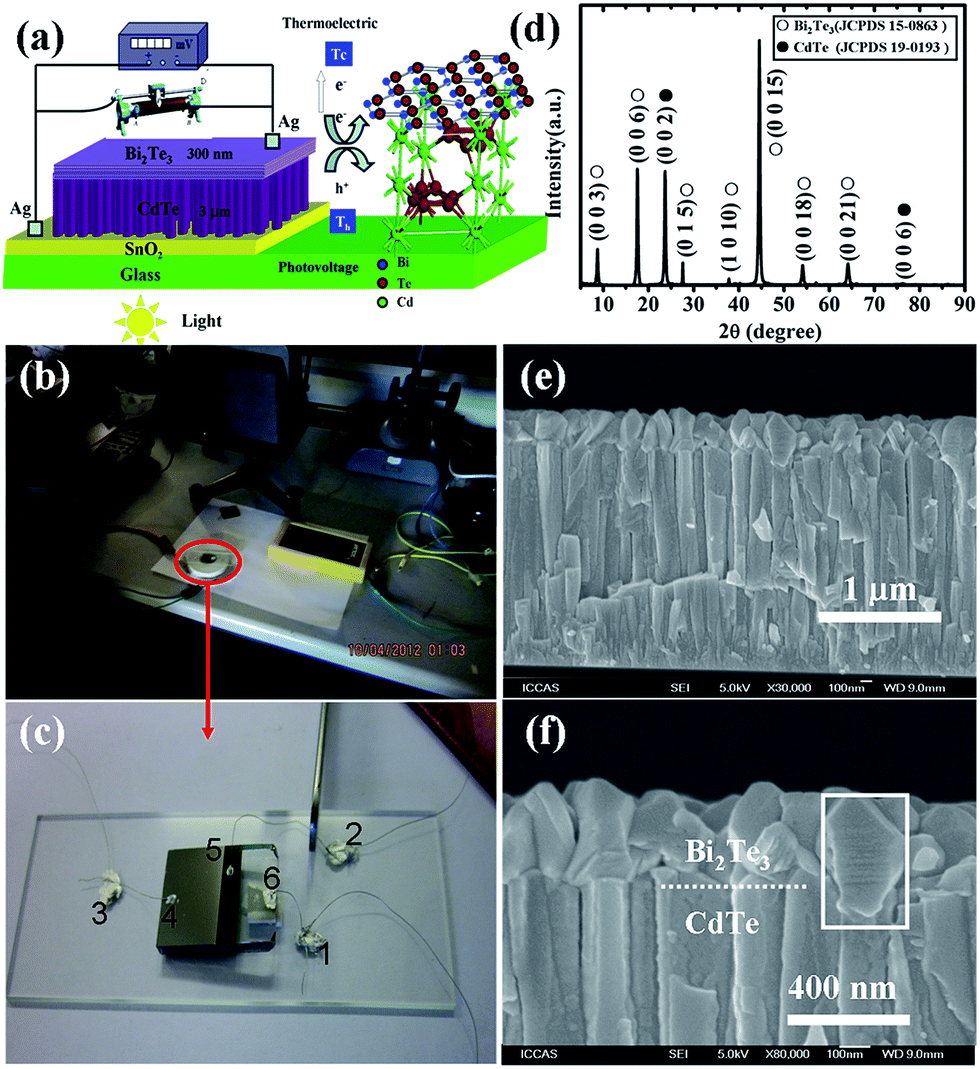 | ||
| Fig. 1 (a) Schematic of the novel cell based on p-CdTe nanorod array/n-Bi2Te3 nanostructure; (b) the image of practical measurement scene; (c) the image of practical sample treated with Ag paste electrode; (d) XRD patterns of CdTe/Bi2Te3 single cell, the CdTe nanorod arrays and layered Bi2Te3 are in (00l) orientation; (e) SEM cross-sectional images of CdTe/Bi2Te3; (f) magnified section of CdTe/Bi2Te3 in (e). | ||
Fig. 1(b) and (c) are the image of practical measurement scene and the sample, respectively. The electrodes of the sample are prepared by the Ag paste. The value of the resistance between point 1 and 6 (label as R16) is 0.2 Ω, the values of R25 and R34 are both 0.1 Ω, which ensures the ohmic contact. The crystal structures of the thin film heterojunction (CdTe/Bi2Te3 sputtering time 90/60 min) are investigated by X-ray diffraction (XRD), as shown in Fig. 1(d). Compared with standard data (JCPDS No. 19-0193), only two characteristic diffraction peaks, (002) and (006), can be attributed to the wurtizite phase of CdTe, which reveals that CdTe in the heterojunction has grown along the c-axis perpendicular to the substrate with good crystalline quality. The other seven peaks, indexed as (003), (006), (015), (1010), (0015), (0018), and (0021), correspond to Bi2Te3 standard data (JCPDS No. 15-0863). The strongest peak, (0015), reveals that Bi2Te3 is in (00l) orientation. No peaks corresponding to impurity materials can be found in Fig. 1(d), which indicates a success in obtaining a CdTe/Bi2Te3 single cell with preferably oriented nanostructure. Fig. 1(e) shows a typical SEM cross-sectional image of a CdTe/Bi2Te3 heterojunction prepared using magnetron sputtering for 90 and 60 minutes, respectively. The junction consists of a layered structure of Bi2Te3 with an average thickness of about 300 nm on the top of an array of CdTe nanorods with an average length of about 3 μm. The diameter of the CdTe nanorods is approximately 150 nm. A more detailed image of the junction interface between CdTe and Bi2Te3 is shown in Fig. 1(f). A gapless transition between CdTe and Bi2Te3 layers indicates that a CdTe/Bi2Te3 heterojunction has been prepared successfully.
Due to the band gap large difference between Bi2Te3 and CdTe, the formation junction need to be verified and investigated by the I–V curve. As shown in Fig. 2(a), the shape of the I–V curve is not a straight line and it is different with the traditional p–n junction as staggered pattern, which shows that an special p–n junction is formed. The measurement process can be expressed to an equivalent circuit, as shown in lower inset of Fig. 2(a). When the positive current import in the cell from Bi2Te3 to FTO, the same current lead to a higher voltage value in light state than that of dark state. Because the xenon light illuminate in the same direction from FTO, this phenomenon is caused by the current with same direction produced by the PV effect. Meanwhile, the TE effect is negligible here due to the temperature here only 3 K from FTO (302.15 K) and Bi2Te3 (299.15 K). Based on the constant direction of light illumination, the reverse current import in the cell from FTO to Bi2Te3 will lead to a higher voltage value in dark state than that of light state. Then, the current import in greater scope from −100 mA to 100 mA is used to investigate the I–V curve, as shown in Fig. 2(b). In the positive range, the same current import bring the similar voltage, it can be explained by the import current is much higher than the PV and TE synergy. Meanwhile, the current import from top to bottom of Bi2Te3 (n-type) can help heat transfer from bottom to top of Bi2Te3, in this way, the temperature gradient can not easy to establish, and the TE effect are not remarkable in light or dark state. On the contrary, when the negative current imported, the temperature gradient from bottom to top of Bi2Te3 will establish the TE effect. Meanwhile, the TE effect of dark state will higher than that of light state due to the PV effect in light state. Therefore, the same current lead to a higher voltage value in light state than that of dark state. However, with the imported current increase to −100 mA, the voltage of light state and dark state is become similar finally.
 | ||
| Fig. 2 I–V curve of CdTe/Bi2Te3 single cell (a) the value of the import current from −6 mA to 10 mA; (b) the value of the import current from −100 mA to 100 mA. The light state is illuminated using xenon light source at 8 mW cm−2 and the device was illuminated from the conductive substrate side. The imported current is first from Bi2Te3 to FTO and then current reversal. The lower inset is the equivalent circuit schematic diagram of the measurement process. | ||
In this work, V–t plots are employed to distinguish the PV from the TE effect based on the fact that the response time of the photoelectric effect is much faster than that of the TE effect. A photovoltage can be generated almost instantaneously once the light is illuminating the junction, while the Seebeck voltage builds up relatively slowly depending on the rate of the process to establish a temperature difference across the material. Fig. 3 shows the V–t results of the CdTe/Bi2Te3 single cell. Xenon light and halogen light were used as the light sources to illuminate the cell. Xenon light generates less heat than halogen light at the same light intensity. The V–t curves of CdTe/Bi2Te3 single cell are obtained by the xenon light with an illumination intensity of 8 mW cm−2, 25 mW cm−2 and 50 mW cm−2, respectively, as shown in Fig. 3(a)–(c). The dark voltage at t = 0 s is −3 μV, as shown in Fig. 3(a). When the light is switched on, the cell rapidly generates a photovoltage of 119 μV which then decreases slowly to 113 μV irregularly. In this case, the voltage generated by the TE effect is not clearly observed during the light illumination. This can be attributed to the low power of xenon light with less heat generation. When the light is turned off, the voltage quickly decreases to 8 μV and then it takes 46 seconds to return to the dark voltage. The time required to return to the dark voltage suggests that a small Seebeck voltage has been generated due to the production of heat in the cell during the illumination process. Fig. 3(b) shows the results of the same device for an increased illumination intensity to 25 mW cm−2. The dark voltage at t = 0 s is −12 μV. When the light is turned on, the voltage increases to 402 μV rapidly, this is higher than the voltage in Fig. 3(a) due to higher illumination intensity. However, the voltage decreases with time during the continuous illumination. This can be explained by a well-established fact that the photovoltage of a PV cell decreases with increasing its junction temperature. It appears that the heat generated from xenon light illumination of 25 mW cm−2 is not sufficient to establish a temperature difference to produce a Seebeck voltage that compensates a decrease in photovoltage due to an increase in the operating temperature. It is interesting to note that the time required to return to the dark voltage decreased to 18 s and the voltage continues to decrease to reach −23 μV for another 51 s. To investigate this hypothesis, the illumination intensity is increased to 50 mW cm−2 and the corresponding V–t curve is shown in Fig. 3(c). The dark voltage at 0 s becomes −5 μV. When the light is turned on, the voltage increases to 842 μV due to the higher illumination intensity. However, the voltage continues to increase during illumination. We believe that in this case the heat produced from xenon light is sufficient to generate a Seebeck voltage to over-compensate the photovoltage decrease due to an increase in operating temperature. As a result, the total voltage generated is increased due to combined PV–TE effects in a single cell. Due to more heat generated, it takes 100 seconds to return to the dark voltage when the light is switched off.
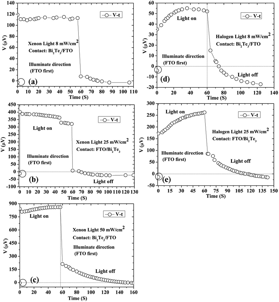 | ||
| Fig. 3 Voltage change as a function of time (V–t plots) for CdTe/Bi2Te3 single cell illuminated using xenon light source at (a) 8 mW cm−2; (b) 25 mW cm−2; (c) 50 mW cm−2; and using halogen light source at (d) 8 mW cm−2; (e) 25 mW cm−2. The light was turned on at 0 s and turned off at approximately 60 s. The first point is the background voltage generated by ambient light. The device was illuminated from the conductive substrate side. | ||
In an attempt to confirm this interesting observation, the halogen lamp was used to carry out comparative experiments under the same conditions. Since the halogen light contains a large ratio of infrared spectrum to visible light than that of xenon light, it is anticipated that the Seebeck voltage will be more significant under halogen illumination. Fig. 3(d) and (e) show the V–t curves of the same CdTe/Bi2Te3 single cell tested using the halogen light with an illumination intensity of 8 mW cm−2 and 25 mW cm−2, respectively. As shown in Fig. 3(d), the dark voltage at 0 s is −4 μV. When the light is switched on, the voltage increases to 35 μV, which is smaller than that in Fig. 3(a) because the halogen light consists of significantly less visible light than that in a xenon light under the same illumination intensity. Similar to the trend seen in Fig. 3(c), the voltage continues to increase under illumination. When the light is switched off, the voltage immediately drops to 15 μV and maintains at around this value for about 4 s before it slowly decreases with time. The time required to return to the dark voltage is longer than that shown in Fig. 3(a). In addition, the rate of decrease is also faster than that in Fig. 3(a) as indicated by the slope of the lines. Clearly, when the heat generation increases in the cell, the simultaneous PV–TE effects can be easily observed as in Fig. 3(d). The Seebeck voltage is more significant if the halogen light intensity is increased to 25 mW cm−2 as shown in the Fig. 3(e). The photovoltage under this illumination intensity is 172 μV, while the voltage increase due to the TE effect is more than 100 μV.
To further confirm this results and understand the junction better, the light illuminated direction from Bi2Te3 with the same experimental method is also been investigated. The similar results are shown in Fig. S1 (ESI†) excepting the comparation between the PV and TE can be observed in Fig. S1(c) and (d).† Meanwhile, the I–V and P–V curve of the CdTe/Bi2Te3 single cell are shown in Fig. S2 (ESI†) and verified the phenomenon of PV and TE synergy again.
The TE effect of CdTe/Bi2Te3 single cell is investigated by the heat import method. Fig. 4(a) is the schematic of the TE effect measurement method, the light is transformed to heat by the light-proof Cu and the temperature test points are at the middle area of Bi2Te3 and FTO, respectively. Fig. 4(b) is the V–ΔT curve of the CdTe/Bi2Te3 single cell from 27 K to 63 K, the result shows that the voltage induced from the TE effect is increasing with the ΔT enhancement and the TE effect is verified here. The value of ΔT as 27 K is corresponding to the voltage of TE effect is 0.8 mV and the voltage of TE effect become 2.5 mV with the ΔT increase to 63 K. The ΔT with two times enhancement seems to achieve the three times increase of TE voltage. However, based on the constant ZT value of Bi2Te3, the slope of the V–ΔT curve is decrease with the ΔT, as shown in Fig. 4(b). Generally, the thermal condition will limit the thermoelectric property of Bi2Te3 membrane, especially for the thin thickness of 300 nm. The data of ΔT from 52.2 K to 62.8 K in Fig. 4(b) are collected from the cool and hot side without cooling device and the concrete data are shown in Table S1.† As shown in Table S1,† the increase rate of Tcool is much lower than that of Thot under the thermal input by the copper. It is seems that the Bi2Te3 in this manuscript can solve some problems of heat without cooling device. The I–V and P–V curve based on the TE effect are also investigated by the multimeter combined with a slide rheostat to form a parallel circuit. The slide rheostat was enhanced to a larger resistance by fixed step and the results are shown in Fig. 4(c) and (d). Fig. 4(c) is the I–V and P–V curve of the fixed ΔT at 27 K, and the maximum voltage is 0.8 mV and the maximum power output is 160 pW with the voltage and current at 400 μV and 0.4 μA, respectively. Fig. 4(d) is the I–V and P–V curve of the fixed ΔT at 41 K, and the maximum voltage is 1.5 mV and the maximum power output is 490 pW with the voltage and current at 700 μV and 0.7 μA, respectively. The data in Fig. 4(c) and (d) are collected from the cooling device with the temperature plus and minus 0.5 K using the cycling water with fixed temperature. The shape of the curve in Fig. 4(c) and (d) are not regular enough comparing with the traditional TE device reported in our previous work due to the special junction.7 However, the TE effect is verified here and the value of power output and open circuit voltage can be adjusted by the ΔT.
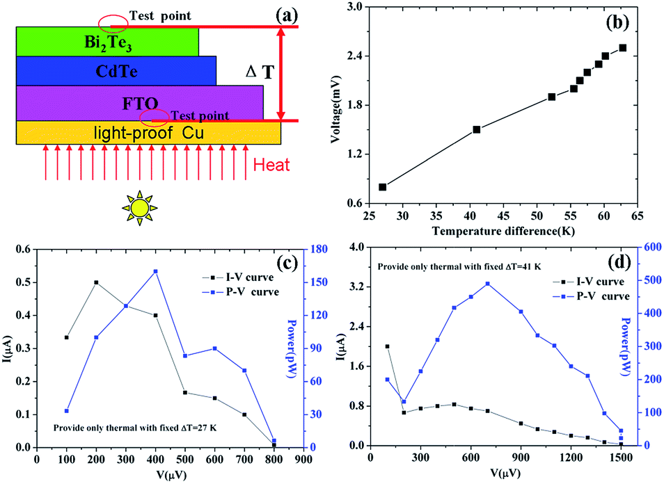 | ||
| Fig. 4 (a) Schematic of the TE effect measurement method; (b) voltage change as a function of temperature difference (V–ΔT plots) for CdTe/Bi2Te3 single cell from 27 K to 63 K; (c) the I–V and P–V curve of CdTe/Bi2Te3 single cell at the fixed ΔT as 27 K; ΔT as 41 K (d). The light was transferred to heat by the light-proof Cu and the temperature test point is at the middle area of Bi2Te3 and FTO, respectively. | ||
In a general way, the power output of PV is much larger than that of TE under the same simulated solar light. Therefore, the observation the TE effect in PV effect is difficulty. Herein, using the CdTe without CdCl2 activation to form the CdTe/Bi2Te3 single cell is successful to understand the synergy relationship between PV and TE effect. Then, the FTO/CdS/CdTe/Bi2Te3 cell with the CdCl2 activation has been prepared and investigated. The SEM image of the cell is shown in Fig. S3 (ESI†). The property of the cell is investigated by the standard measurement method excepting the light lasting time and the results are shown in Table 1. As seen from the Table 1, when the cell initial illuminated by the light, the cell parameters of Voc, Jsc, FF and η are 0.38 V, 14.54 mA cm−2, 33.24 and 2.02%, respectively. With the light continuous illuminating for 1 min, the cell parameters of Voc, Jsc, FF and η attain 0.410 V, 15.16 mA cm−2, 40.33 and 2.49%, respectively. Obviously, the PV and TE synergy has increased the efficiency from 2.02 to 2.49 and make the η increased by 23.3%. When the light continuous illuminating for 2 min, the cell parameters keep essentially constant as the η increased by 21.8%. Then, the data are collected from the prolong light illumination for 3 min and 4 min, respectively. The light continuous illuminating for 3 min, the η is increased by 32.7% and the 34.2% is corresponding to continuous illuminating for 4 min. It is anticipated that the η will continue increase during the range of temperature application of Bi2Te3. In this way, the PV and TE synergy can be applied to single cell to improve the overall efficiency of reality solar cell.
| Cell | Time/s | Voc/V | Jsc/mA cm−2 | FF | η (%) | Δη | Δη/η |
|---|---|---|---|---|---|---|---|
| 1 | 0 | 0.38 | 14.54 | 33.24 | 2.02 | — | — |
| 60 | 0.410 | 15.16 | 40.33 | 2.49 | 0.47 | 23.3% | |
| 120 | 0.408 | 15.12 | 39.85 | 2.46 | 0.44 | 21.8% | |
| 180 | 0.440 | 16.32 | 36.95 | 2.68 | 0.66 | 32.7% | |
| 240 | 0.450 | 16.39 | 36.56 | 2.71 | 0.69 | 34.2% |
In conclusion, our experimental results demonstrate that a simultaneous PV–TE effect has been observed in a single heterojunction of CdTe/Bi2Te3. This innovative integration of PVs and TEs proves to be beneficial in two aspects: (1) both effects work together in the “same direction” to enhance the output voltage of the cell by harvesting the sun radiation from visible and infrared spectrum, respectively (i.e., realization of full-solar spectrum energy harvesting in a single cell); (2) the TE effect in this novel cell utilizes the “waste infrared spectrum” to generate the Seebeck voltage that helps to compensate the output voltage reduction with increasing temperature in a conventional solar cell, leading to the possibility of developing solar cells with high operating temperatures. Based on the synergistic photovoltaic and thermoelectric effect, the cell of FTO/CdS/CdTe/Bi2Te3 has the η increased by 23.3% after 1 min illumination. The successful synergy of PVs and TEs in a single cell of CdTe/Bi2Te3 heterojunction is anticipated to provide a novel technological route towards developing a next generation of high efficiency solar energy devices which have the capability to harvest solar energy from a wider solar spectrum.
Experimental
Synthesis of CdTe nanorod arrays
CdTe nanorod arrays were prepared using a Magnetron Sputtering System (JGP-450a, SKY Technology Development Co., Ltd Chinese Academy of Sciences) on a clean conducting glass substrate (fluorine doped tin oxide (FTO), 14 Ω per square, Nippon Sheet Glass Group, Japan). A hot-pressed CdTe target (99.99%) was used with the radio frequency (RF) power of 84 W. The deposition was carried out under the following conditions: the temperature of substrate was 350 °C; the base pressure of the deposition chamber was set to 3.0 × 10⁻⁴ Pa or below and the working pressure of the chamber was set to 0.4 Pa; the sputtering gas was supplied by a flow of Ar at 25 sccm; and the deposition time of CdTe was between 50 and 90 minutes.Synthesis of CdTe/Bi2Te3 nanorod arrays/nanolayer
The as-synthesized CdTe nanorod arrays on conducting glass was then used as a substrate for deposition of the Bi2Te3 nanolayers using the same magnetron sputtering system. A hot-pressed Bi2Te3 target (99.99%) and Te target (99.99%) (purchased from General Research Institute for Nonferrous Metals, China) were used for co-sputtering to compensate tellurium sublimation at high temperature. The distance between targets and substrate was maintained at 90 mm. A direct current (DC) power of 20 W was supplied to the Bi2Te3 target, while a RF power of 40 W was supplied to the Te target.Before deposition, the FTO substrate was cleaned in turn using acetone, alcohol, and deionized water for 15 min in an ultrasonic bath. The base pressure of the deposition chamber was set to 3.0 × 10⁻⁴ Pa or below and the working pressure of the chamber was set to 2.0 Pa; the sputtering gas was provided by a flow of Ar at 25 sccm. The deposition time of Bi2Te3 was between 60 and 90 minutes. After deposition, the thin films were annealed in situ at 350 °C (substrate temperature) for 20 minutes in Ar atmosphere.
Electric contacts were prepared by attaching a wire to the top Bi2Te3 and the bottom FTO layers respectively using Ag paint (RS). The voltage was measured between these two wires.
Synthesis of FTO/CdS/CdTe/Bi2Te3 cell
The FTO/CdS/CdTe solar cell was prepared using a magnetron sputtering system. Briefly, a commercial 60 mm diameter hot-pressed CdS target (purchased from General Research Institute for Nonferrous Metals, China) was used and the distance between targets and substrates maintained at 90 mm. The CdS film was deposited at 1.0 Pa, 30 W, 30 min and 450 °C. Meanwhile, a commercial 60 mm diameter hot-pressed CdTe target (purchased from General Research Institute for Nonferrous Metals, China) was used and the distance between targets and substrates maintained at 90 mm. The CdTe film was deposited at 0.4 Pa, 84 W, 90 min and 450 °C. The CdTe was treated by CdCl2 saturated solution and annealed in the over. At last, a commercial 60 mm diameter hot-pressed Bi2Te3 target (Sb heavy doping) (99.99%) was used and the distance between targets and substrates maintained at 90 mm. The Bi2Te3 film was deposited at 1.0 Pa, 30 W, 30 min and room temperature.Characterization and measurements
The microstructures and morphologies of CdTe/Bi2Te3 junction were analyzed by X-ray diffraction (XRD, Rigaku Dmax 2200) and Scanning Electron Microscopy (SEM, JEOL JSM 6700F). The voltage of the cell was measured using a Keithley 2000 Multimeter combined with a slide rheostat to form a parallel circuit, the slide rheostat was set to a maximum resistance of 100![[thin space (1/6-em)]](https://www.rsc.org/images/entities/char_2009.gif) 000 Ω and the light intensity of xenon and halogen lamps were adjusted to 8 mW cm−2, 25 mW cm−2 and 50 mW cm−2 at room temperature, respectively. The intensity of the light sources was determined using an irradiance meter (Solar Survey 100, Seaward Electronics, UK). The current with positive and negative from 0.1–1 mA (step with 0.1 mA) and 1–10 mA (step with 1 mA) are used to investigate the I–V curve of CdTe/Bi2Te3 single cell under the dark and xenon light with 8 mW cm−2 intensity, respectively.
000 Ω and the light intensity of xenon and halogen lamps were adjusted to 8 mW cm−2, 25 mW cm−2 and 50 mW cm−2 at room temperature, respectively. The intensity of the light sources was determined using an irradiance meter (Solar Survey 100, Seaward Electronics, UK). The current with positive and negative from 0.1–1 mA (step with 0.1 mA) and 1–10 mA (step with 1 mA) are used to investigate the I–V curve of CdTe/Bi2Te3 single cell under the dark and xenon light with 8 mW cm−2 intensity, respectively.
The voltage of TE effect are also investigated by the multimeter combined with a slide rheostat to form a parallel circuit. The slide rheostat was enhanced to a larger resistance by fixed step. The heat source is provided by the light-proof Cu transferring from the halogen light illumination. The fixed ΔT as 27 K and 41 K are created by the cooling device with the temperature plus and minus 0.5 K using the cycling water. When the fixed ΔT as 27 K, the temperature of hot and cool side are 324.55 K and 297.55 K, respectively. When the fixed ΔT as 41 K, the temperature of hot and cool side are 340.15 K and 299.15 K, respectively.
The parameters of the FTO/CdS/CdTe/Bi2Te3 cell are investigated by the traditional method with a solar-simulated light source (AM1.5 G filtered, 100 mW cm−2, 69911, Oriel) and Keithley 2000 Multimeter.
Acknowledgements
The work was supported by the State Key Development Program for Basic Research of China (Grant No. 2012CB933200), the State Key Program of National Natural Science Foundation of China (Grant No. 61534001), National Natural Science Foundation of China (Grant No. 51602299) and the Fundamental Research Funds for the Central Universities.Notes and references
- T. F. Schulze and T. W. Schmidt, Energy Environ. Sci., 2015, 8, 103 CAS.
- M. Roeb and H. Muller-Steinhagen, Science, 2010, 329, 773 CrossRef CAS PubMed.
- R. S. Aga, D. Jowhar, A. Ueda, Z. Pan, W. E. Collins, R. Mu, K. D. Singer and J. Shen, Appl. Phys. Lett., 2007, 91, 232108 CrossRef.
- E. Skoplaki and J. A. Palyvos, Sol. Energy, 2009, 83, 614 CrossRef CAS.
- D. Kraemer, B. Poudel, H.-P. Feng, J. C. Caylor, B. Yu, X. Yan, Y. Ma, X. Wang, D. Wang, A. Muto, K. McEnaney, M. Chiesa, Z. Ren and G. Chen, Nat. Mater., 2011, 10, 532 CrossRef CAS PubMed.
- M. Tan, Y. Deng, Y. Wang, Z. W. Zhang, H. M. Liang and J. Y. Yang, Sens. Actuators, A, 2011, 171, 252 CrossRef CAS.
- M. Tan, Y. Deng, Y. Wang, B. W. Luo, L. X. Liang and L. L. Cao, J. Electron. Mater., 2012, 41, 3031 CrossRef.
- L. D. Zhao, G. Tan, S. Hao, J. He, Y. Pei, H. Chi, H. Wang, S. Gong, H. Xu, V. P. Dravid, C. Uher, G. J. Snyder, C. Wolverton and M. G. Kanatzidis, Science, 2015, 6269, 351 Search PubMed.
- Y. Deng, W. Zhu, Y. Wang and Y. M. Shi, Sol. Energy, 2013, 88, 182 CrossRef.
- X. Z. Guo, Y. D. Zhang, D. Qin, Y. H. Luo, D. M. Li, Y. T. Pang and Q. B. Meng, J. Power Sources, 2010, 195, 7684 CrossRef CAS.
- N. Wang, L. Han, H. C. He, N. H. Park and K. Koumoto, Energy Environ. Sci., 2011, 4, 3676 CAS.
- T. Chen, G. H. Gong, W. H. Hu, J. X. Zhu, H. B. Yang, Q. Y. Yan and C. M. Li, Energy Environ. Sci., 2012, 5, 6294 CAS.
- Y. Y. Dou, F. Wu, L. Fang, G. B. Liu, C. Y. Mao, K. Wan and M. Zhou, J. Power Sources, 2016, 307, 181 CrossRef CAS.
- K. Wan, F. Wu, Y. Y. Dou, L. Fang and C. Y. Mao, J. Alloys Compd., 2016, 680, 373 CrossRef CAS.
- B. W. Luo, Y. Deng, Y. Wang, M. Tan, L. L. Cao and W. Zhu, CrystEngComm, 2012, 14, 7922 RSC.
- G. Stechmann, S. Zaefferer, P. Konijnenberg, D. Raabe, C. Gretener, L. Kranz, J. L. Perrenoud, S. Buecheler and A. N. Tiwari, Sol. Energy Mater. Sol. Cells, 2016, 151, 66 CrossRef CAS.
- Y. Deng, H. M. Liang, Y. Wang, Z. W. Zhang, M. Tan and J. L. Cui, J. Alloys Compd., 2011, 509, 5683 CrossRef CAS.
- Y. Deng, Z. W. Zhang, Y. Wang and Y. B. Xu, J. Nanopart. Res., 2012, 14, 775 CrossRef.
Footnote |
| † Electronic supplementary information (ESI) available. See DOI: 10.1039/c6ra20149k |
| This journal is © The Royal Society of Chemistry 2016 |