
 Open Access Article
 This Open Access Article is licensed under a Creative Commons Attribution-Non Commercial 3.0 Unported Licence
Effect of PCBM nanoparticles in lead-based layered (PEA)2PbI4 perovskite thin films†
Deepak Aloysius ,
Muskan Khan,
Arindam Mondal and
Satyajit Gupta*
,
Muskan Khan,
Arindam Mondal and
Satyajit Gupta*
Department of Chemistry, Indian Institute of Technology Bhilai, Durg, Chhattisgarh 491002, India. E-mail: satyajit@iitbhilai.ac.in; deepakaloysius@iitbhilai.ac.in; muskankhanj@iitbhilai.ac.in; arindamm@iitbhilai.ac.in
First published on 12th August 2024
Abstract
Two-dimensional (2D) layered halide perovskites are considered to be one of the future potential semiconductor materials due to their higher moisture stability than three-dimensional (3D) perovskites. However, improving their optical and electrical properties is still necessary for critical applications. The technique of additive engineering can be utilized to tune and enhance the optoelectrical properties of the 2D perovskites. This work studies the impact of mixing a certain amount of a fullerene derivative ‘[6,6]-phenyl C61-butyric acid methyl ester’ (PCBM) into 2D (PEA)2PbI4 perovskite thin films (PEA = phenyl ethyl ammonium). The studies show that PCBM does not affect the structure and bandgap of the (PEA)2PbI4 perovskite. On the other hand, PCBM improves photoluminescence emission intensity and promotes charge separation at the perovskite/PCBM interface. Further studies convey that, even though PCBM can heal certain defect states in the (PEA)2PbI4 perovskite material, the electrons generated under intense illumination at the perovskite/PCBM interface are trapped by this fullerene derivative. Hence, PCBM plays a dual role when mixed with the (PEA)2PbI4 perovskite, as (1) a defect healing agent and (2) an electron acceptor. However, over continuous illumination on the (PEA)2PbI4 perovskite thin films, the photoexcited electrons are trapped by PCBM. As a result, the photocurrent response and the photocatalytic reaction rate get reduced in PCBM mixed (PEA)2PbI4 perovskite thin films.
Introduction
The successive developments in APbX3 type [A = inorganic monocations such as caesium ions (Cs+) and organic monocations such as methyl ammonium (CH3NH3+), etc., X = halides such as iodide (I−), bromide (Br−), mixed halides or pseudohalides such as thiocyanate (SCN−), etc.1–6] perovskite semiconductors made them one of the promising candidates among third-generation solar cell devices.7 Furthermore, the report of Cao et al. on two-dimensional (2D) halide perovskites opened the path toward another class of perovskite semiconductors.8 Along with the existing properties of 3D perovskites, such as a high absorption coefficient,9 intense photoluminescence10 etc., the main advantage of 2D perovskites is their relatively higher moisture stability.11 The large hydrophobic organic cations in 2D perovskites act as a barrier for moisture intervention.12 However, the wide optical bandgap13 and low charge transport14 are the major drawbacks of 2D perovskites. The technique of additive engineering has been utilized in 3D perovskites to enhance their optoelectronic properties.15–20 In 2D perovskites, optoelectrical properties can be fine-tuned using the same additive engineering technique.21 Earlier, Zhang et al. reported that Cs+ doping in (BA)2(MA)3Pb4I13 perovskite solar cells boosts the power conversion efficiency (PCE) by more than 1% with better humidity resistance.22 Furthermore, Zhang et al. reported that after MACl doping, the BA2MA4Pb5I16 layered perovskite films showed improved PCE and operational stability.23 This work studies the effect of mixing a fullerene derivative ‘[6,6]-phenyl C61-butyric acid methyl ester’ (PCBM) nanoparticles into a 2D perovskite.Several research groups have already established using PCBM nanoparticles in organic solar cells to facilitate exciton separation.24–26 The high solubility and the electron-accepting nature are the significant properties that promote the use of PCBM in photovoltaic materials.27 After the establishment of perovskite photovoltaics, PCBM is used as an electron transport layer (ETL) in perovskite solar cell devices. You et al. reported the fabrication of CH3NH3PbI3−xClx based flexible solar cell devices using PCBM as the ETL and achieved a PCE of 9.2%.28 Heo et al. reported the fabrication of MAPbI3 based perovskite solar cells with PCBM as the ETL, which has an average PCE of 18.1%.29 Similarly, there have been several reports on using the PCBM ETL in low-temperature processed perovskite solar cell devices with p–i–n architecture.30–34 Furthermore, some reports show the effect of the PCBM layer interface on 2D perovskite films. Yang et al. reported that at the (PEA)2(MA)n−1PbnI3n+1/PCBM interface, the phenethylammonium iodide (PEAI) ligand promotes better transfer of electrons from perovskite crystals to the PCBM layer.35 Shen et al. reported efficient and fast charge transfer dynamics in 2D CsPbBr3 nanosheets and PCBM layer heterojunctions.36 Wei et al. reported efficient charge separation at a multiple quantum well (MQW) perovskite/PCBM interface.37
This work reports the effect of mixing varying amounts of PCBM nanoparticles in the (PEA)2PbI4 perovskite [where the phenylethylammonium ion (PEA+) is the organic cation], which has not been reported before to the best of our knowledge. Even though (PEA)2PbI4 perovskites have firmly bound excitons,38 it is observed that PCBM helps in the separation of excitons at the PCBM/perovskite interface in the mixed form. Furthermore, we found that PCBM cannot influence the structure and bandgap of the (PEA)2PbI4 perovskite. On the other hand, PCBM improves the photoluminescence emission intensity and reduces the charge carrier lifetime.
Experimental section
Materials
Lead iodide (99%), 2-phenylethylamine solution (≥99%), hydroiodic acid (57 wt% in H2O, distilled, stabilized, 99.95%), dimethyl sulfoxide (ACS reagent, ≥99.9%), N,N-dimethyl formamide (ACS reagent, ≥99.8%), toluene (99.8%), PCBM (>99.5%), tetrabutylammonium hexafluorophosphate [(Bu4N)+(PF6)−] (≥98%), dichloromethane (anhydrous, ≥99.8%), 2-mercaptobenzothiazole (97%), hexane (anhydrous, 95%), hypophosphorous acid solution (50 wt% in H2O), titanium isopropoxide (97%), diethanolamine (reagent grade, ≥98%), and diethyl ether (≥99.9%) were purchased from Sigma-Aldrich. Triphenylphosphine oxide (>98%) was purchased from Spectrochem, and silica was purchased from Loba Chemie. Acetone (99.9%) was purchased from Rankem. Ethanol (99.9%) and plain glass slides were purchased from a local supplier. FTO (fluorine-doped tin oxide) coated glass slides were purchased from Feeniks Technologies (transparency >85%). All the chemicals were used without further purification.Material characterization
The perovskite thin films were fabricated using the EZspin-A1 Apex Spin Coater. Grazing incidence X-ray diffraction (GIXRD) analysis was done with the Bruker D8 Advance X-ray diffractometer using Cu ‘Kα’ radiation of wavelength 1.54 Å at 40 mA current and 40 kV potential. The UV-visible spectroscopy analysis was conducted using Shimadzu UV-2600. Furthermore, the steady state photo-luminescence (SSPL) analysis was carried out using Fluorolog FL3-211 HORIBA Scientific with a 450-watt Xenon arc lamp. Time-resolved photoluminescence (TRPL) analysis was carried out using the HORIBA Scientific DeltaFlex™ and DeltaPro™ Fluorescence Lifetime Systems using a 453 nm laser excitation pulse (EZTime software was used for TRPL analysis). The field emission scanning electron microscope (FESEM) images of the perovskite thin films were captured using Zeiss Gemini SEM500 instruments. The high-resolution transmission electron microscopy (HRTEM) images were captured using JEOL and JEM-F200 (CF-HR). The photoelectrochemistry-related experiments are carried out using a Metrohm Dropsens μStat-i 400s potentiostat (with the Dropview 8400 software). The perovskite thin film was illuminated using a calibrated solar simulator (Model, ScienceTech) with a light intensity equivalent to one sun (1.5 AM). Also, the photocatalytic experiments were conducted using a white light emitting diode (LED) source. All analyses are performed over perovskite thin films fabricated over glass substrates, except for the photoelectrochemical analyses where the FTO substrate was used.Synthesis of phenylethylammonium iodide (PEAI)
The equimolar concentration of phenylethyl amine solution and hydroiodic acid (HI) was neutralized in 10 ml ethanol medium at low temperature (ice bath). 1 ml of hypophosphorous acid solution (H3PO2) was added to prevent the oxidation of iodide ions. The reaction was allowed to proceed for 4 hours, and a white powder of PEAI was obtained after the solvent (ethanol) was evaporated, followed by washing (with diethyl ether), filtering, and drying.Synthesis of PCBM mixed (PEA)2PbI4 perovskite precursor solution
A 2![[thin space (1/6-em)]](https://www.rsc.org/images/entities/char_2009.gif) :1 molar ratio of PEAI and lead iodide (PbI2) was dissolved in the mixture of N,N-dimethyl formamide (DMF), and dimethyl sulfoxide (DMSO) solvents in the ratio 8:2 under constant stirring for 4 hours at 60 °C. An orange solution was obtained. A thoroughly dispersed PCBM solution (in the same solvent ratio as the precursor solution) was added to the perovskite precursor solution as per the composition and further sonicated for 1 hour. The PCBM nanoparticles occupy as spherical aggregates when dispersed in the solvent mixture (Fig. S1, ESI†).
:1 molar ratio of PEAI and lead iodide (PbI2) was dissolved in the mixture of N,N-dimethyl formamide (DMF), and dimethyl sulfoxide (DMSO) solvents in the ratio 8:2 under constant stirring for 4 hours at 60 °C. An orange solution was obtained. A thoroughly dispersed PCBM solution (in the same solvent ratio as the precursor solution) was added to the perovskite precursor solution as per the composition and further sonicated for 1 hour. The PCBM nanoparticles occupy as spherical aggregates when dispersed in the solvent mixture (Fig. S1, ESI†).
Fabrication of PCBM mixed (PEA)2PbI4 perovskite thin films
Both glass slides (2.5 cm × 2 cm) and FTO films (2 cm × 2 cm) were used as substrates for thin film fabrication. The substrates were cleaned with soap and sonicated in distilled water, acetone, and ethanol for 10 minutes each. Furthermore, the substrates were dried under a hot air gun. These cleaned substrates were preheated at 90 °C for 5 minutes. Then, the substrates were loaded in a spin coater, and 200 μl of precursor solution was spread over the glass substrates (150 μl precursor solution was used for the FTO substrates). After that, the perovskite thin films were fabricated via spin coating at 4000 rpm for 20 seconds. The antisolvent toluene was added at the 15th second. The perovskite thin films were heated at 100 °C for 10 minutes in the last step.Synthesis and fabrication of a compact titania layer (c-TiO2)
An equimolar mixture (0.5 M) of titanium isopropoxide [Ti(OCH(CH3)2)4] and diethanolamine [NH(CH2CH2OH)2] was dissolved in ethanol (5 ml) by rigorous stirring for 15 minutes. The solution turns from white to colorless. The resulting solution was spin-coated over the FTO substrate at 7000 rpm for 30 seconds, and then annealed at 500 °C for 2 hours.Results and discussion
Structure and bandgap
PCBM nanoparticle mixed (PEA)2PbI4 perovskite thin films are fabricated via a one-step spin coating technique. A uniform thin film was obtained for all the compositions over the substrate (Fig. S2, ESI†). In this work, the thin films fabricated using the following precursor solutions are analyzed: P0 = pristine (PEA)2PbI4, P0.5 = 0.5 mg PCBM mixed in 1 ml (PEA)2PbI4 perovskite precursor, and P0.75 = 0.75 mg PCBM mixed in 1 ml (PEA)2PbI4 perovskite precursor solution.GIXRD of all compositions (P0, P0.5, and P0.75) was carried out to determine the polycrystalline structure. The diffraction data show periodic peaks along (00l) planes (Fig. 1a), which signifies the layered orientation of PbI42− moieties in (PEA)2PbI4 perovskite thin films (Fig. 1b).39 Also, no peak shift is observed in all the compositions, which indicates that PCBM does not affect the (PEA)2PbI4 perovskite structure.
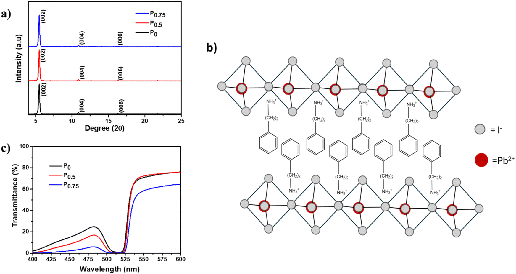 | ||
| Fig. 1 (a) XRD analysis of P0, P0.5, and P0.75 perovskite thin films. (b) Layered structure of the (PEA)2PbI4 perovskite. (c) Transmittance analyses of P0, P0.5, and P0.75 compositions. [P0 = pristine (PEA)2PbI4, P0.5 = 0.5 mg PCBM mixed in 1 ml (PEA)2PbI4 perovskite precursor, and P0.75 = 0.75 mg PCBM mixed in 1 ml (PEA)2PbI4 perovskite precursor solution.] | ||
Furthermore, all compositions of (PEA)2PbI4 perovskite thin films show significant absorption in the visible region of the spectrum (Fig. S3, ESI†). Also, an increase in absorbance is observed for P0.5 and P0.75 compositions. This observation indicates that the black PCBM is evenly dispersed over the (PEA)2PbI4 perovskite thin films. Furthermore, the bandgap of all compositions (P0, P0.5, and P0.75) was calculated from the Tauc plot using the Kubelka–Munk function [(αhν)2 vs. hν, where ‘α’ is the absorption coefficient] using transmittance data (Fig. 1c). It was observed that the bandgap remains at 2.36 eV for all compositions (Fig. S4a–c, ESI†). Therefore, the PCBM mixing does not create structural distortion in (PEA)2PbI4 perovskite thin films.
Morphological and optical properties
The surface morphology and thickness of the PCBM nanoparticle mixed (PEA)2PbI4 perovskite thin films were analyzed using SEM images (Fig. 2a–c). This analysis shows that the perovskite films are packed and pinhole-free. Also, the thickness of the films is within the range of 450 nm to 500 nm. On analyzing the film morphology, the P0 composition generates more uniform films, and the roughness increases at the surface of the PCBM nanoparticle mixed (PEA)2PbI4 perovskite thin films (P0.5 and P0.75).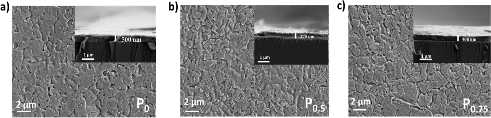 | ||
| Fig. 2 Surface and cross-sectional images (given in the inset) of (a) P0, (b) P0.5, and (c) P0.75 compositions. [P0 = pristine (PEA)2PbI4, P0.5 = 0.5 mg PCBM mixed in 1 ml (PEA)2PbI4 perovskite precursor, and P0.75 = 0.75 mg PCBM mixed in 1 ml (PEA)2PbI4 perovskite precursor solution.] | ||
The steady state photo luminescence (SSPL) analysis was carried out to understand charge carrier recombination intensity in the PCBM nanoparticle mixed (PEA)2PbI4 perovskite thin films (Fig. 3a). The emission peak of all the compositions (P0, P0.5, and P0.75) is observed at the same wavelength of 529 nm, which agrees with the bandgap calculated from the Tauc plots (Fig. S4a–c, ESI†). On the other hand, an increase in emission intensity is observed for P0.5 and P0.75 compositions. The higher PL intensity is attributed to the passivation of defect states over the PCBM nanoparticle mixed (PEA)2PbI4 perovskite films. Earlier, several reports show improvement in PL intensity due to defect passivation on different perovskite materials.40,41 The (PEA)2PbI4 perovskites are reported to have undercoordinated Pb2+ ions on the surface and I− defects in the bulk due to iodide migration.42 Here, PCBM can passivate the defects by binding them at the grain boundaries and help in electron movement across the grains.43 The P0.5 composition has the highest PL intensity, which indicates that it is the optimum composition, showing the most defect passivation. A similar increase in PL intensity can also be observed when triphenylphosphine oxide (TOPO) is mixed in the (PEA)2PbI4 perovskite thin films (Fig. S5a, ESI†). In TOPO, the lone pair electrons in the oxygen atom replace the iodide vacancies.44 Conversely, the PL intensity remains unaffected with neutral materials such as silica particle mixed (PEA)2PbI4 perovskite films (Fig. S5b, ESI†). These analyses indicate that additive engineering techniques can influence the defect states in (PEA)2PbI4 perovskite thin films.
 | ||
| Fig. 3 (a) SSPL and (b) TRPL curves of P0, P0.5 and P0.75 compositions. [P0 = pristine (PEA)2PbI4, P0.5 = 0.5 mg PCBM mixed in 1 ml (PEA)2PbI4 perovskite precursor, and P0.75 = 0.75 mg PCBM mixed in 1 ml (PEA)2PbI4 perovskite precursor solution]. | ||
The time-resolved photo luminescence (TRPL) analysis was carried out to understand the charge recombination dynamics in the PCBM nanoparticles mixed (PEA)2PbI4 perovskite thin films (Fig. 3b). The average lifetime of the compositions is determined by fitting TRPL curves using the biexponential decay function [y = A1exp(−t/τ1) + A2exp(−t/τ2)]. Here, the average lifetime of P0 (τ = 246 ps) is higher than that of P0.5 (τ = 216 ps) and P0.75 (τ = 195 ps). The fitting data are given in Table S1 (ESI†). Here, PCBM plays the role of an electron acceptor by collecting the excited electrons from the (PEA)2PbI4 perovskite, thereby reducing the charge recombination lifetime. Upon analysis of the SSPL and TRPL data for PCBM nanoparticle mixed (PEA)2PbI4 perovskite compositions, the SSPL intensity increases for P0.5 and P0.75 compared to P0. On the other hand, the TRPL lifetime decreases for P0.5 and P0.75 compared to P0. This trend is due to the dual behavior of PCBM in the (PEA)2PbI4 perovskite: as a defect healing agent (from SSPL analysis) and as an electron acceptor (from TRPL analysis).
Photoelectrochemical properties
The photoelectrochemical analysis was conducted to study the charge carrier dynamics of PCBM nanoparticle mixed (PEA)2PbI4 perovskite thin films within a multilayer system. The analysis was carried out using a three-electrode setup with ‘Ag/AgCl’ as the reference electrode, ‘Pt’ wire as the counter electrode, and the multilayered perovskite thin film as the working electrode (Fig. S6, ESI†). Along with that, 0.1 M [(Bu4N)+(PF6)−] dissolved in dichloromethane (DCM) solvent was used as the supporting electrolyte, and a calibrated solar stimulator of 1 sun intensity functioned as the light source. The thin films are fabricated as glass/FTO/c-TiO2/perovskite multilayers and illuminated from the glass side at a 10 cm distance from the solar simulator.Initially, the chronoamperometric analysis was carried out for 3 minutes by chopping light at 0 V applied bias with respect to the Ag/AgCl reference electrode (Fig. 4a). The study shows that a stable and significantly higher current is generated for P0 (8.5 μA cm−2) than for P0.5 (3.8 μA cm−2) and P0.75 (1.6 μA cm−2) compositions. A similar trend was observed for chronoamperometry analysis without the cTiO2 layer (Fig. S7a–c, ESI†). Furthermore, the linear sweep voltammetry (LSV) analysis under illumination over the potential range of −0.2 V to 0.6 V shows a higher current response for P0 composition (Fig. 4b). So, it is evident that the PCBM traps the photogenerated charge carriers from the (PEA)2PbI4 perovskite thin film and prevents its further movement within the system. Apart from that, the LSV curve signifies that the PCBM improves the open circuit potential (Voc) of the (PEA)2PbI4 perovskite thin film (Fig. 4b, inset). The improved Voc is attributed to the defect passivation effect of PCBM, as observed from SSPL analysis (discussed earlier in Fig. 3a). Earlier reports on different perovskite materials suggest the improvement of Voc through defect healing.45
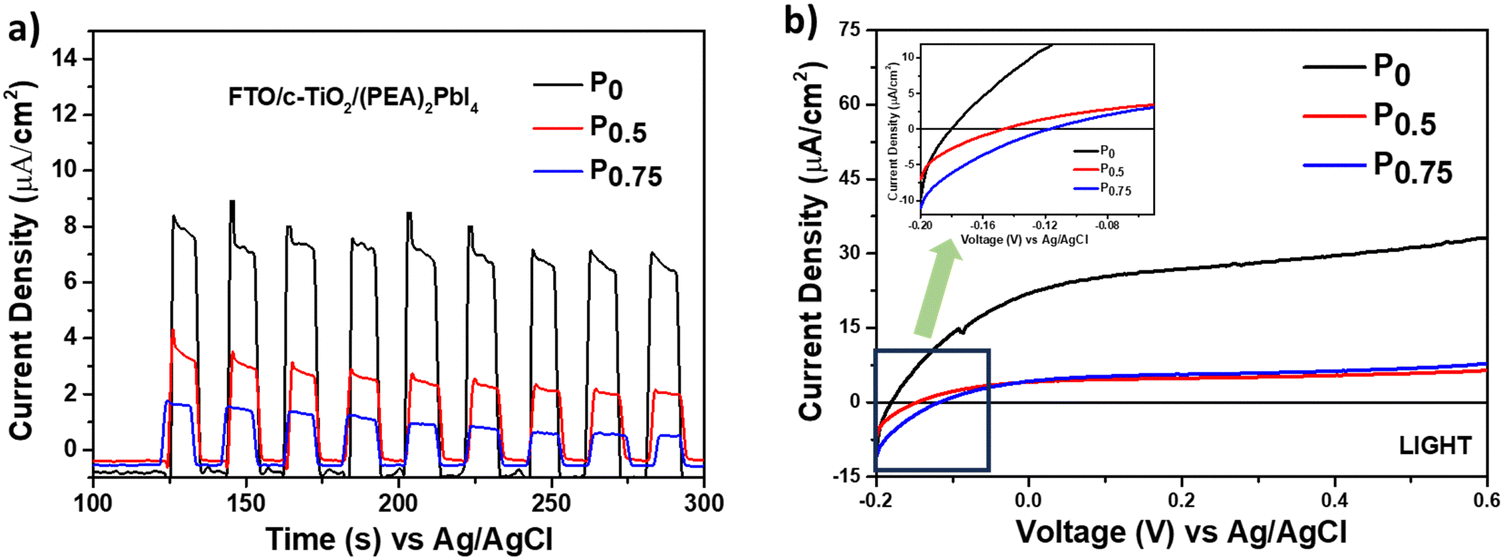 | ||
| Fig. 4 (a) The chronoamperometric and (b) LSV curves (over c-TiO2) of P0, P0.5, and P0.75 compositions. [P0 = pristine (PEA)2PbI4, P0.5 = 0.5 mg PCBM mixed in 1 ml (PEA)2PbI4 perovskite precursor, and P0.75 = 0.75 mg PCBM mixed in 1 ml (PEA)2PbI4 perovskite precursor solution.] | ||
Photocatalytic properties
The photocatalytic activity of PCBM nanoparticle mixed (PEA)2PbI4 perovskite thin films was studied on 2-mercaptobenzothiazole (MBT) dye to understand the behavior of excitons within the material. The photocatalytic experiment was carried out with perovskite thin films coated over a glass slide. A strip of a perovskite thin film-coated glass slide (2 cm × 0.5 cm) was dipped in the MBT dye-filled quartz cuvette and illuminated with a white LED. Furthermore, the absorbance of the MBT dye was analyzed every 15 minutes for three cycles.The MBT dye undergoes an oxidative S–S coupling reaction under illumination in the presence of the perovskite photocatalyst, forming 2,2′-dithiobis(benzothiazole) (MBTS).46,47 The holes generated from the (PEA)2PbI4 perovskite excitation catalyze the coupling reaction.48 The photocatalysis reaction rate of each composition is directly correlated with the reduction absorption peak intensity at each 15-minute interval (Fig. S8, ESI†). Furthermore, the rate constant (k) was determined from the slope of the 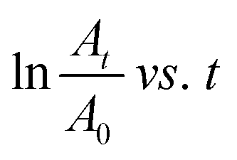 plot where A denotes the absorbance and t denotes the irradiation time (Fig. 5). The absorbance analysis shows that the photocatalytic S–S coupling reaction rate is higher for the P0 (0.055 min−1) composition than the P0.5 (0.04 min−1) and P0.75 (0.041 min−1) compositions. The formation of MBTS was confirmed using the electrospray ionization mass spectroscopy (ESI-MS) analysis of the dye (Fig. S9, ESI†). This observation indicates that relatively fewer holes are available for catalyzing the coupling reaction in PCBM nanoparticle mixed (PEA)2PbI4 perovskite thin film compositions (P0.5 and P0.75). Here, PCBM traps the photoexcited electrons of the (PEA)2PbI4 perovskite and promotes faster recombination with holes. This process eventually reduces the reaction rate due to the decline in excitons of the (PEA)2PbI4 perovskite photocatalyst. Also, the higher roughness of P0.5 and P0.75 thin film compositions can reduce the photocatalysis reaction rate (as observed in Fig. 2).
 | ||
| Fig. 5 Photocatalytic coupling reaction rate of the MBT dye in P0, P0.5, and P0.75 compositions at 15-minute intervals (the MBT coupling reaction is given in the inset). [P0 = pristine (PEA)2PbI4, P0.5 = 0.5 mg PCBM mixed in 1 ml (PEA)2PbI4 perovskite precursor, and P0.75 = 0.75 mg PCBM mixed in 1 ml (PEA)2PbI4 perovskite precursor solution]. | ||
Conclusions
This work delineates the effect of PCBM nanoparticle mixing in (PEA)2PbI4 perovskite thin films with three different compositions (P0, P0.5, and P0.75). All the compositions form a layered structure with the same bandgap. However, roughness increases for PCBM mixed (PEA)2PbI4 perovskite thin film compositions (P0.5 and P0.75). Also, the SSPL emission intensity increases considerably for P0.5 and P0.75 compositions, which indicates that PCBM helps passivate the defect states at the grain boundaries. On the other hand, the TRPL analysis indicates that the recombination lifetime declined for P0.5 and P0.75 compositions, which is attributed to PCBM's electron-accepting behavior. The discrepancy in the increase in SSPL intensity and the decrease in TRPL lifetime signifies the two independent behaviors of PCBM nanoparticles impacting (PEA)2PbI4 perovskite thin film properties transiently. Furthermore, the photoelectrochemistry analysis shows a significant reduction in the current generation in P0.5 and P0.75 compositions, even though there is an increase in Voc due to defect passivation. Also, in the photocatalytic analysis, the reaction rate is lower for P0.5 and P0.75 compositions. All these observations signify that the PCBM traps the accepted electrons on continuous illumination on (PEA)2PbI4 perovskite thin films.Data availability
The data supporting this article have been included as part of the ESI.†Conflicts of interest
The authors declare no competing financial interest.Acknowledgements
DA acknowledges the Ministry of Education, India (MoE), for the research fellowship. SG thanks SERB for the Start-up Research Grant (SRG/2019/000157).References
- Y. Pan, Y. Zhang, W. Kang, N. Deng, Z. Yan, W. Sun, X. Kang and J. Ni, Mater. Adv., 2022, 3, 4053–4068 RSC.
- M. A. Green, A. Ho-Baillie and H. J. Snaith, Nat. Photonics, 2014, 8, 506–514 CrossRef CAS.
- H.-S. Kim, C.-R. Lee, J.-H. Im, K.-B. Lee, T. Moehl, A. Marchioro, S.-J. Moon, R. Humphry-Baker, J.-H. Yum, J. E. Moser, M. Grätzel and N.-G. Park, Sci. Rep., 2012, 2, 591 CrossRef PubMed.
- M. Kulbak, S. Gupta, N. Kedem, I. Levine, T. Bendikov, G. Hodes and D. Cahen, J. Phys. Chem. Lett., 2016, 7, 167–172 CrossRef CAS PubMed.
- D. P. McMeekin, G. Sadoughi, W. Rehman, G. E. Eperon, M. Saliba, M. T. Hörantner, A. Haghighirad, N. Sakai, L. Korte, B. Rech, M. B. Johnston, L. M. Herz and H. J. Snaith, Science, 1979, 351, 151–155 CrossRef PubMed.
- Q. Jiang, D. Rebollar, J. Gong, E. L. Piacentino, C. Zheng and T. Xu, Angew. Chem., Int. Ed., 2015, 54, 7617–7620 CrossRef CAS PubMed.
- J. Yan and B. R. Saunders, RSC Adv., 2014, 4, 43286–43314 RSC.
- D. H. Cao, C. C. Stoumpos, O. K. Farha, J. T. Hupp and M. G. Kanatzidis, J. Am. Chem. Soc., 2015, 137, 7843–7850 CrossRef CAS PubMed.
- H. Wang, J. Ma and D. Li, J. Phys. Chem. Lett., 2021, 12, 8178–8187 CrossRef CAS PubMed.
- S. Chen and G. Shi, Adv. Mater., 2017, 29, 1605448 CrossRef PubMed.
- I. C. Smith, E. T. Hoke, D. Solis-Ibarra, M. D. McGehee and H. I. Karunadasa, Angew. Chem., Int. Ed., 2014, 53, 11232–11235 CrossRef CAS PubMed.
- S. Yang, Y. Wang, P. Liu, Y.-B. Cheng, H. J. Zhao and H. G. Yang, Nat. Energy, 2016, 1, 15016 CrossRef CAS.
- E.-B. Kim, M. S. Akhtar, H.-S. Shin, S. Ameen and M. K. Nazeeruddin, J. Photochem. Photobiol., C, 2021, 48, 100405 CrossRef CAS.
- F. Zhang, H. Lu, J. Tong, J. J. Berry, M. C. Beard and K. Zhu, Energy Environ. Sci., 2020, 13, 1154–1186 RSC.
- A. Mahapatra, D. Prochowicz, M. M. Tavakoli, S. Trivedi, P. Kumar and P. Yadav, J. Mater. Chem. A Mater., 2020, 8, 27–54 RSC.
- T. Li, Y. Pan, Z. Wang, Y. Xia, Y. Chen and W. Huang, J. Mater. Chem. A Mater., 2017, 5, 12602–12652 RSC.
- F. Zhang and K. Zhu, Adv. Energy Mater., 2020, 10, 1902579 CrossRef CAS.
- Y. Wu, F. Xie, H. Chen, X. Yang, H. Su, M. Cai, Z. Zhou, T. Noda and L. Han, Adv. Mater., 2017, 29, 1701073 CrossRef PubMed.
- D. S. Mann, S. Thakur, S. S. Sangale, K.-U. Jeong, S.-N. Kwon and S.-I. Na, Sol. Energy Mater. Sol. Cells, 2024, 269, 112768 CrossRef CAS.
- K. Nagasawa, T. Sano, V. N. Chau, K. Enomoto, Y. Okuyama, Y. Sayama, R. Oikawa, T. Chiba and J. Kido, Adv. Mater. Interfaces, 2024, 11, 2300449 CrossRef CAS.
- G. Grancini and M. K. Nazeeruddin, Nat. Rev. Mater., 2018, 4, 4–22 CrossRef.
- X. Zhang, X. Ren, B. Liu, R. Munir, X. Zhu, D. Yang, J. Li, Y. Liu, D.-M. Smilgies, R. Li, Z. Yang, T. Niu, X. Wang, A. Amassian, K. Zhao and S. (Frank) Liu, Energy Environ. Sci., 2017, 10, 2095–2102 RSC.
- F. Zheng, C. Zuo, M. Niu, C. Zhou, S. J. Bradley, C. R. Hall, W. Xu, X. Wen, X. Hao, M. Gao, T. A. Smith and K. P. Ghiggino, ACS Appl. Mater. Interfaces, 2020, 12, 25980–25990 CrossRef CAS PubMed.
- F. Padinger, R. S. Rittberger and N. S. Sariciftci, Adv. Funct. Mater., 2003, 13, 85–88 CrossRef CAS.
- T. Erb, U. Zhokhavets, G. Gobsch, S. Raleva, B. Stühn, P. Schilinsky, C. Waldauf and C. J. Brabec, Adv. Funct. Mater., 2005, 15, 1193–1196 CrossRef CAS.
- Y. Kim, S. A. Choulis, J. Nelson, D. D. C. Bradley, S. Cook and J. R. Durrant, Appl. Phys. Lett., 2005, 86, 063502 CrossRef.
- C. J. Brabec, A. Cravino, D. Meissner, N. S. Sariciftci, T. Fromherz, M. T. Rispens, L. Sanchez and J. C. Hummelen, Adv. Funct. Mater., 2001, 11, 374–380 CrossRef CAS.
- J. You, Z. Hong, Y. (Michael) Yang, Q. Chen, M. Cai, T.-B. Song, C.-C. Chen, S. Lu, Y. Liu, H. Zhou and Y. Yang, ACS Nano, 2014, 8, 1674–1680 CrossRef CAS PubMed.
- J. H. Heo, H. J. Han, D. Kim, T. K. Ahn and S. H. Im, Energy Environ. Sci., 2015, 8, 1602–1608 RSC.
- Z. Liu, L. Krückemeier, B. Krogmeier, B. Klingebiel, J. A. Márquez, S. Levcenko, S. Öz, S. Mathur, U. Rau, T. Unold and T. Kirchartz, ACS Energy Lett., 2019, 4, 110–117 CrossRef CAS.
- W. Chen, Y. Wu, J. Liu, C. Qin, X. Yang, A. Islam, Y.-B. Cheng and L. Han, Energy Environ. Sci., 2015, 8, 629–640 RSC.
- C. Tao, S. Neutzner, L. Colella, S. Marras, A. R. Srimath Kandada, M. Gandini, M. De Bastiani, G. Pace, L. Manna, M. Caironi, C. Bertarelli and A. Petrozza, Energy Environ. Sci., 2015, 8, 2365–2370 RSC.
- F. Fu, T. Feurer, T. Jäger, E. Avancini, B. Bissig, S. Yoon, S. Buecheler and A. N. Tiwari, Nat. Commun., 2015, 6, 8932 CrossRef CAS PubMed.
- C.-H. Chiang and C.-G. Wu, Nat. Photonics, 2016, 10, 196–200 CrossRef CAS.
- J. Yang, S. Xiong, J. Song, H. Wu, Y. Zeng, L. Lu, K. Shen, T. Hao, Z. Ma, F. Liu, C. Duan, M. Fahlman and Q. Bao, Adv. Energy Mater., 2020, 10, 2000687 CrossRef CAS.
- Y. Shen, D. Yu, X. Wang, C. Huo, Y. Wu, Z. Zhu and H. Zeng, Nanotechnology, 2018, 29, 085201 CrossRef PubMed.
- Y. Wei, M. Li, R. Li, L. Zhang, R. Yang, W. Zou, Y. Cao, M. Xu, C. Yi, N. Wang, J. Wang and W. Huang, Appl. Phys. Lett., 2018, 113, 041103 CrossRef.
- H. Fang, J. Yang, S. Adjokatse, E. Tekelenburg, M. E. Kamminga, H. Duim, J. Ye, G. R. Blake, J. Even and M. A. Loi, Adv. Funct. Mater., 2020, 30, 1907979 CrossRef CAS.
- D. B. Mitzi, J. Mater. Chem., 2004, 14, 2355 RSC.
- Yukta, M. K. Chini, R. Ranjan and S. Satapathi, ACS Appl. Electron Mater., 2021, 3, 1572–1582 CrossRef CAS.
- S. A. Fateev, D. E. Belikova, P. A. Ivlev, N. A. Belich, K. A. Lyssenko, E. G. Maksimov, E. A. Goodilin and A. B. Tarasov, Chem. Mater., 2022, 34, 2998–3005 CrossRef CAS.
- J. Yin, R. Naphade, L. Gutiérrez Arzaluz, J.-L. Brédas, O. M. Bakr and O. F. Mohammed, ACS Energy Lett., 2020, 5, 2149–2155 CrossRef CAS.
- J. Xu, A. Buin, A. H. Ip, W. Li, O. Voznyy, R. Comin, M. Yuan, S. Jeon, Z. Ning, J. J. McDowell, P. Kanjanaboos, J.-P. Sun, X. Lan, L. N. Quan, D. H. Kim, I. G. Hill, P. Maksymovych and E. H. Sargent, Nat. Commun., 2015, 6, 7081 CrossRef CAS PubMed.
- W. Li, X. Lai, F. Meng, G. Li, K. Wang, A. K. K. Kyaw and X. W. Sun, Sol. Energy Mater. Sol. Cells, 2020, 211, 110527 CrossRef CAS.
- S. Wu, J. Zhang, Z. Li, D. Liu, M. Qin, S. H. Cheung, X. Lu, D. Lei, S. K. So, Z. Zhu and A. K.-Y. Jen, Joule, 2020, 4, 1248–1262 CrossRef CAS.
- D. Cardenas-Morcoso, A. F. Gualdrón-Reyes, A. B. Ferreira Vitoreti, M. García-Tecedor, S. J. Yoon, M. Solis de la Fuente, I. Mora-Seró and S. Gimenez, J. Phys. Chem. Lett., 2019, 10, 630–636 CrossRef CAS PubMed.
- W.-B. Wu, Y.-C. Wong, Z.-K. Tan and J. Wu, Catal. Sci. Technol., 2018, 8, 4257–4263 RSC.
- A. Mondal, A. Lata, A. Prabhakaran and S. Gupta, Mater. Adv., 2021, 2, 5712–5722 RSC.
Footnote |
| † Electronic supplementary information (ESI) available: Perovskite thin film images. UV absorbance data. TEM and SSPL analyses. TRPL fitting data. Additional details on photoelectrochemical experiments, and photocatalytic reaction with ESI-MS results. See DOI: https://doi.org/10.1039/d4ya00338a |
| This journal is © The Royal Society of Chemistry 2024 |