
 Open Access Article
 This Open Access Article is licensed under a Creative Commons Attribution-Non Commercial 3.0 Unported Licence
First demonstration of 2T0C-FeDRAM: a-ITZO FET and double gate a-ITZO/a-IGZO FeFET with a record-long multibit retention time of >4-bit and >2000 s†
Tae Hyeon
Noh‡
 a,
Simin
Chen‡
a,
Hyo-Bae
Kim
b,
Taewon
Jin
a,
Seoung Min
Park
a,
Seong Ui
An
a,
Xinkai
Sun
a,
Jaekyun
Kim
a,
Jae-Hoon
Han
c,
Ji-Hoon
Ahn
*b,
Dae-Hwan
Ahn
*c and
Younghyun
Kim
*a
a,
Simin
Chen‡
a,
Hyo-Bae
Kim
b,
Taewon
Jin
a,
Seoung Min
Park
a,
Seong Ui
An
a,
Xinkai
Sun
a,
Jaekyun
Kim
a,
Jae-Hoon
Han
c,
Ji-Hoon
Ahn
*b,
Dae-Hwan
Ahn
*c and
Younghyun
Kim
*a
aDepartment of Photonics and Nanoelectronics, BK21 FOUR ERICA-ACE Center, Hanyang University, Ansan 15588, Republic of Korea. E-mail: younghyunkim@hanyang.ac.kr
bDepartment of Materials Science and Chemical Engineering, Hanyang University, Ansan, Republic of Korea
cKorea Institute of Science and Technology, Seoul, Republic of Korea
First published on 19th August 2024
Abstract
Conventional DRAM, consisting of one transistor and one capacitor (1T1C), requires periodic data refresh processes due to its limited retention time and data-destructive read operation. Here, we propose and demonstrate a novel 3D-DRAM memory scheme available with a single transistor and a single ferroelectric field-effect transistor (FeFET) DRAM (2T0C-FeDRAM), which offers extended retention time and non-destructive read operation. This architecture uses a back-end-of-line (BEOL)-compatible amorphous oxide semiconductor (AOS) that is suitable for increasing DRAM cell density. Notably, the device structures of a double gate a-ITZO/a-IGZO FeFET, used for data storage and reading, are engineered to achieve an enlarged memory window (MW) of 1.5 V and a prolonged retention time of 104 s. This is accomplished by a double gate and an a-ITZO/a-IGZO heterostructure channel to enable efficient polarization control in hafnium-zirconium oxide (HZO) layers. We present successful program/erase operations of the double gate a-ITZO/a-IGZO FeFET through incremental step pulse programming (ISPP), demonstrating multi-level states with remarkable retention characteristics. Most importantly, we perform 2T0C-FeDRAM operations by electrically connecting the double gate a-ITZO/a-IGZO FeFET and the a-ITZO FET. Leveraging the impressive performance of the double gate a-ITZO/a-IGZO FeFET technology, we have effectively showcased an exceptionally record-long retention time exceeding 2000 s and 4-bit multi-level states, positioning it as a robust contender among emerging memory solutions in the era of artificial intelligence.
Introduction
Dynamic random-access memory (DRAM) serves as the primary memory device in modern computing systems owing to its remarkable features, such as high speed, low power dissipation, and high integration density. However, the inherent leakage current of DRAM poses limitations on its role as a prolonged storage option, necessitating the frequent execution of a data refresh process to restore the data to its original state.1–3 It is worth noting that the refresh process leads to a significant portion of the power consumption during DRAM operation.4,5 For improving the 1T1C DRAM performance, the raised capacitor with a high height has been adopted to retain a sufficiently large capacitance.6 Additionally, the dimension scaling down of a write transistor (Wtr) has been performed to improve the operation speed. However, the increased aspect ratio of the raised capacitor and the scaling of the Wtr technology have encountered physical limitations, constraining the number of DRAM cells per chip. In addition, current DRAM technologies cannot address the issue of limited retention time caused by a sneak path of Si MOSFETs.7,8 Meanwhile, an amorphous oxide semiconductor (AOS) two transistors (2T) DRAM to enhance the data retention time and enable the non-destructive read operation has been proposed to tackle these issues.9,10 The AOS 2T0C-DRAM with a back-end-of-line (BEOL) availability can offer a 3D integration to effectively increase DRAM cell density through a vertical stacking process. In addition, the AOS transistors have the advantage of a low leakage current, thanks to the superior material properties of AOS, resulting in improved retention time.11–13 For high bandwidth memory (HBM) processing-in-memory, AOS 2T0C-DRAM could be one of the breakthrough technologies for energy efficiency and memory density because it provides fewer data refresh operations and the capability of 3D integration, essential for AI accelerators.14 Recently, the AOS 2T0C-DRAM has been researched in this aspect and improved retention time and multi-bit operations have been reported.15–17 However, due to the leakage current caused by the Wtr of the AOS 2T0C-DRAM, the gradual reduction in voltage stored at the storage node (VSN) results in a current of read bit line (IRBL) degradation. Moreover, the retention time of AOS 2T0C-DRAM is still insufficient to dramatically reduce power consumption caused by data refresh processes in terms of AI accelerator applications.4,18 Additionally, it degrades the read operation margin characteristics, impairing multi-bit operation.15,16To address this issue, we focused on the Hf-based ferroelectric field effect transistor (FeFET) featuring non-volatile memory behavior, low-power operation, fast switching speed, and excellent reliability. In the FeFET, the memory state can be modulated by spontaneous ferroelectric polarization, which can be maintained for a long time after the programming pulse is applied to the gate.19–21 This behavior could allow multi-bit operations for the AOS-based 2T0C-FeDRAM, enabling applications in non-volatile memory and neuromorphic devices.22,23 Furthermore, AOS-based FeFETs possess superior reliability due to excellent Hafnium-Zirconium Oxide (HZO)/AOS interface properties, while Si FeFETs suffer from charge trapping issues because of the poor interface properties of HZO/Si.24 Therefore, AOS channel-based FeFETs show promising potential for high-density, low-power DRAM applications.25,26
In this work, we propose the AOS-based 2T0C-FeDRAM consisting of an a-ITZO FET with an Al2O3 gate insulator and a double gate a-ITZO/a-IGZO FeFET as a Wtr and a ferroelectric read transistor (FE-Rtr), respectively. Fig. 1(a) shows the key challenges and key advantages of the proposed 2T0C-FeDRAM in comparison with the traditional IGZO 2T0C-DRAM. In the existing 2T0C-DRAM, where data is maintained by storing charge in the storage node (SN), setting VSN to 0 V results in the inability to preserve data. On the other hand, thanks to its non-volatility in storing the threshold voltage (Vth), our proposed 2T0C-FeDRAM scheme, which maintains the voltage between the source and drains in the Wtr at 0 V, minimizes the leakage current of the Wtr. This leads to ultra-long retention time with negligible IRBL variation. In addition, the significantly reduced leakage current in the Wtr provides a better multi-bit read margin.15,16 We utilize the partial polarization of FeFETs as read transistors (Rtr) to minimize charge loss and reduce IRBL degradation. Also, the improved gate bias stability enabled by an optimized hetero a-ITZO/a-IGZO structure helps to suppress IRBL degradation. Fig. 1(b) shows the concept of structure for the proposed 3-dimensional channel-all-around (CAA) AOS-based 2T0C-FeDRAM memory array. Details of process flow can be found in the ESI in Fig. S1.† The CAA structure enables 3D integration and is beneficial for scaling. Increased electric field applied to the HZO layer while scaling enhances polarization switching efficiency and enables multilayer stacking at a lower aspect ratio.27 A BEOL process-compatible AOS channel with high mobility and a low thermal budget (<320 °C) is utilized to enable 3D integration for next-generation memory, essential for low-power processing-in-memory applications in AI technology.
 | ||
| Fig. 1 (a) The key challenges and key advantages of the proposed 2T0C-FeDRAM in comparison with the traditional IGZO 2T0C DRAM. This proposed 2T0C-FeDRAM mainly highlights: (1) the FeFET read transistor can adjust and store the Vth after applying voltage, which enables operation at VSN = 0 V; (2) non-overlapping IRBL characteristics are achievable owing to the reduction of the leakage current of Wtr prolonged retention times, facilitating diverse multi-bit benefits; (3) to mitigate additional IRBL degradation from Vth variation caused by poor stress stability, an optimized hetero a-ITZO/a-IGZO structure with superior stress stability can significantly reduce IRBL degradation while enhancing retention time. (b) Concept of structure and features for the proposed 3-dimensional CAA AOS-based 2T0C-FeDRAM memory array. | ||
Experimental
Before the demonstration of the AOS-based 2T0C-FeDRAM as illustrated in Fig. 2(a), we fabricated W/a-IGZO/a-ITZO/HZO/P+ Si MSFM ferroelectric capacitors to verify that the ferroelectric polarization properties of the HZO by atomic layer deposition (ALD) as shown in Fig. 2(b). First, a P+ Si (1019 cm−3) substrate was ultrasonically wet-cleaned in acetone and isopropanol. The HZO films (10 nm) were deposited by ALD using Cp-based cocktail precursor (Hf[Cp(NMe2)3] + Zr[Cp(NMe2)3]) and ozone.28 Then, an a-ITZO/a-IGZO was deposited as a semiconductor layer for MSFM ferroelectric capacitors. Finally, top metals with W (50 nm) were deposited and patterned to measure the electrical characteristics of ferroelectric capacitors.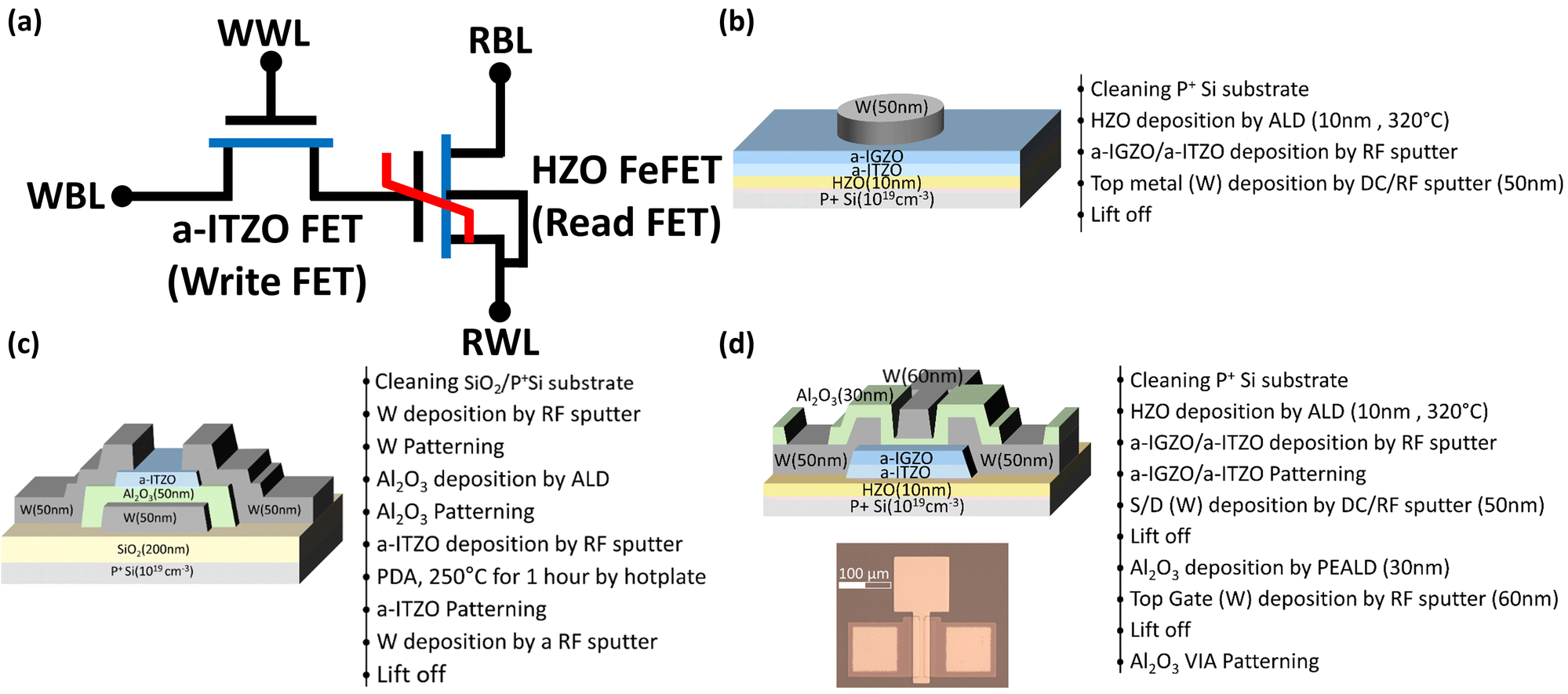 | ||
| Fig. 2 (a) Layout of the AOS-based 2T0C-FeDRAM cell with schematic device structure and fabrication process flow of (b) W/a-IGZO/a-ITZO/HZO/P+ Si MSFM ferroelectric capacitors. (c) The a-ITZO FET as a Wtr and (d) the double gate W/Al2O3/a-IGZO/a-ITZO FeFET as FE-Rtr. | ||
Next, we fabricated the a-ITZO FET as a Wtr. Fig. 2(c) shows the fabrication process flow of the Wtr. First, a SiO2 (200 nm)/P+ Si (1019 cm−3) substrate was ultrasonically wet-cleaned in acetone and isopropanol. Then, W (50 nm) was deposited and patterned as a bottom gate by RF sputter. The Al2O3 films (50 nm) were deposited by ALD and patterned as an insulator layer. A channel layer a-ITZO (10 nm) was deposited by RF sputter and post-deposition annealing (PDA) at 250 °C for 1 hour by hotplate. We optimized the channel thickness to correspondingly adjust the Vth, as shown in Fig. S2.† Finally, source and drain electrodes with W (50 nm) were fabricated through RF sputter. Then, the double gate W/Al2O3/a-IGZO/a-ITZO/HZO/P+ Si FeFETs were fabricated as storage transistors.
Fig. 2(d) shows the fabrication process flow of double gate a-ITZO/a-IGZO FeFETs. The HZO films (10 nm) were deposited on the Si substrate by ALD. The ALD-deposited HZO films at 320 °C present ferroelectricity without an additional post-annealing process and a top stressor layer, because the crystallized HZO films with the orthorhombic phase were directly grown at the optimized deposition temperature.28 Our optimized HZO-deposition technique allows easy fabrication processes and compatibility with the BEOL process, as compared to the previous reports that the crystallization process of ALD-deposited HZO films requires both top and bottom stressor layers and post-annealing processes.29–31 An a-ITZO (4 nm)/a-IGZO (8 nm) channel layer to feature high mobility and stability was deposited by using RF magnetron sputtering and patterning. W (50 nm) was deposited as a source and drain electrodes by RF sputter. A 30 nm-thick Al2O3 top gate insulator was deposited on a-ITZO/a-IGZO channel layer. Finally, top gate electrodes with W (60 nm) were constructed to control the body potential.
To confirm the device structure, transmission electron microscopy (TEM), scanning transmission electron microscopy (STEM), and energy-dispersive X-ray spectroscopy (EDS) images were taken by Tecnai F20 G2 and TitanTM 80-300. Fig. 3(a) shows a TEM image of the channel region for the FeFET. To verify the crystal quality of the HZO and a-ITZO/a-IGZO, high-resolution TEM and STEM were also taken as shown in Fig. 3(b) and (c). There is no significant interfacial layer between a-ITZO and poly-crystalized HZO in the figures, unlike the HZO/Si interface. This will lead to some advantages compared to Si FeFET as discussed later. Significantly, the nano-laminated HZO structure was also observed in the STEM image. The separated layer structure of W/Al2O3/a-IGZO/a-ITZO/Al2O3/HZO/P+ Si substrate FeFET was shown in the EDS analysis as shown in Fig. 3(d).
 | ||
| Fig. 3 Cross-sectional (a) low-magnification and (b) high-magnification TEM, (c) STEM, (d) EDS image of fabricated FeFET. It shows a clear W/Al2O3/a-IGZO/a-ITZO/HZO/P+ Si structure. | ||
Measurement results & discussion
Ferroelectric capacitors
The electrical properties of the W/Al2O3/a-IGZO/a-ITZO/Al2O3/HZO/P+ Si ferroelectric capacitor were evaluated by Keithley 4200 and Keithley 4225-RPM instruments. A triangular waveform at a frequency of 10 kHz was applied to the P+ Si electrodes. Fig. 4(a) and (b) show the polarization–voltage (P–V) curves and the transient current–voltage (I–V) curves of the fabricated W/a-IGZO/a-ITZO/HZO/P+ Si MSFM ferroelectric capacitors, respectively. Counter-clockwise P–V loops were observed in MSFM ferroelectric capacitors, with a voltage range from −4 V to 5.5 V. The remanent polarization (Pr) increases with the widening of the voltage sweep range, enabling the harnessing of partially polarized states for multi-level states. However, in the ferroelectric capacitors, larger polarization switching current peaks and coercive voltages were observed under the positive bias than under the negative bias. These asymmetric polarization characteristics can be attributed to the difference in the work functions of top and bottom electrodes, and different charge injection behaviors arising from the W/a-IGZO/a-ITZO and P+ Si. This results in a differential potential drop across the HZO layer in W/a-IGZO/a-ITZO/HZO/P+ Si MSFM ferroelectric capacitors under negative and positive biases.32 | ||
| Fig. 4 (a) P–V and (b) I–V curves of W/a-IGZO/a-ITZO/HZO/P+ Si MSFM capacitor. (c) Variation of the remanent polarization as a function of the number of cycles. | ||
Fig. 4(c) illustrates the endurance of the W/a-IGZO/a-ITZO/HZO/P+ Si MSFM ferroelectric capacitors. For endurance measurements, we optimized the write voltages to achieve not only superior endurance but also large Pr. While the positive coercive voltage is larger than the negative coercive voltage, we found that a higher negative voltage is required for the stable endurance of MSFM ferroelectric capacitors. This result indicates that the electron trapping/de-trapping process is one of the important keys to stable endurance for W/a-IGZO/a-ITZO/HZO/P+ Si MSFM ferroelectric capacitors.33 Our MSFM ferroelectric capacitors exhibit nearly constant 2Pr values even after 107 cycles by applying asymmetric write pulses with amplitude voltages of −4.4 V and 4.25 V for 10 μs for programming and erasing, respectively. Generally, the polarization of HfO2-based ferroelectric films tends to increase up to a certain number of cycles and then decrease until the breakdown. These phenomena are referred to as wake-up effects and fatigue, respectively.34–36 The wake-up phenomenon occurs as oxygen vacancies migrate to the bulk during initial cycles, inducing a phase transition to the ferroelectric state. Subsequent electric field application further drives these vacancies into the film bulk, thereby reducing voltage asymmetry and enhancing the hysteresis loop. Fatigue arises after prolonged cycling when trapped charges from excessive vacancies obstruct the internal electric field, diminishing ferroelectric properties.37 However, in our research, the HZO ferroelectric thin films, which were implemented without post-annealing processes, effectively inhibited the formation of oxygen vacancies.28 This resulted in exceptionally stable ferroelectric properties, eliminating wake-up effects and significant fatigue for up to 107 cycles. The non-volatile characteristics of HZO materials were validated by their stability under voltage stress, ensuring ultra-long retention times. Further optimization could bring 2T0C-FeDRAM's endurance closer to that of commercial DRAM.38,39
AOS multilayer channel
In our investigation to enhance the retention time of DRAM, we explored the efficacy of using a-ITZO, an amorphous oxide semiconductor, as a channel layer. This material was selected for its high electron mobility and low leakage current, traits crucial for high-performance DRAM applications.40 Nevertheless, a notable challenge emerged regarding the material's stability under operational stress conditions, including positive bias stress (PBS) and negative bias stress (NBS).41,42 In the proposed 2T0C-FeDRAM, Vsn is stored at 0 V, and the gate voltage in Rtr is also 0 V. However, the non-volatile nature of the ferroelectric material in the polarized state induces an internal electric field, even without an external field. Thus, PBS and NBS instability also leads to variability in Vth and degradation of the IRBL in 2T0C-FeDRAM. The instability is attributed to the incorporation of oxygen-related defects, such as oxygen vacancies and loosely-bound oxygen within the oxide semiconductor layer.43 Bias stress generates unfavorable traps as water and oxygen molecules infiltrate the channel layer. Traditionally, the mitigation of these defects and the enhancement of device stability are achieved through surface passivation of the channel or the implementation of a multi-channel layer strategy.44–46 Advancing beyond conventional methodologies, we introduce the application of a heterostructure channel FET, integrating a-ITZO with a-IGZO. As shown in Fig. 5, we present the transfer characteristics of both the a-ITZO single-layer FET and the a-ITZO/a-IGZO FET under stress conditions (Vstress = ±20 V for 3600 s, VDS = 1 V), subjected to PBS and NBS. The heterostructure FETs exhibited significantly enhanced stability under both stress conditions compared to their single-channel counterparts. The deposition of the a-IGZO layer results in the passivation of the a-ITZO channel layer interface, protecting it from humidity, moisture, and oxygen molecules in the air. Also, the band alignment and conduction band offset create a high 2DEG structure near the a-ITZO and a-IGZO boundary, resulting in superior interface properties due to the higher electron concentration at the interface.47 The improved stability is attained by preventing oxygen molecule adsorption on the back-channel surface or minimizing electron trapping at the interface of channel and gate dielectric for PBS and NBS, respectively. The improved stability is attained by minimizing electron trapping at the interface of channel and gate dielectric or preventing oxygen molecule adsorption on the back-channel surface for PBS and NBS, respectively.45 Our optimized hetero a-ITZO/a-IGZO structure marks a pivotal advancement in achieving superior stress stability. This development will not only mitigate IRBL degradation but also significantly enhance the retention time. | ||
| Fig. 5 Transfer characteristics under (a) PBS and (b) NBS for a-ITZO single-layer FET, and (c) PBS and (d) NBS for a-ITZO/a-IGZO FET. Stress conditions: Vstress = ±20 V for 3600 s, VDS = 1 V. Enhanced PBS/NBS stability achieved through reduced electron trapping at the channel/gate dielectric interface or oxygen molecule adsorption at the back-channel surface. | ||
HZO ferroelectric FET
It is crucial to achieve a larger MW, specifically by increasing the Vth difference between the programmed and erased states. However, the AOS-based FeFETs generally show poor erase operation due to insufficient potential drop across the HZO layer, leading to a limited MW.25,32 To mitigate this issue, we introduce the double gate to enhance the potential drop across the HZO layer. Please note that the a-IGZO capping layer in a-ITZO/a-IGZO heterostructure channels also has a benefit for the double gate structure because the Al2O3 passivation on a-IGZO is more stable than that on a-ITZO.48Fig. 6(a) shows drain current–voltage (ID–VG) characteristics of the double gate a-ITZO/a-IGZO FeFET under the floated body and with body potential fixed using the top gate. For the measurement under the floated body, the bottom gate voltage (VB.G) is swept from −4 V to 5.8 V and back to −4 V with the VDS of 0.1 V and the top gate voltage (VT.G) floated. The transistors operate well despite different MWs, exhibiting efficient on/off operation with a steep slope. The reverse current observed from −1.5 V to 1 V is attributed to HZO maintaining a nfegative polarization state under negative voltage, resulting in leakage current from the gate to the drain. When HZO is programmed with a positive gate voltage, the drain current flows positively, indicating that the gate current is induced by the polarization in the HZO. As expected, single gate operation under the floated body shows a limited MW of 0.5 V in the double gate a-ITZO/a-IGZO FeFET. On the other hand, when the body potential is fixed through applying 0 V to the top gate, the double gate a-ITZO/a-IGZO FeFET improves their MW up to 1.5 V. To deeply understand the difference between floated and fixed body potentials, we conducted a simulation study using Sentaurus TCAD simulator. Fig. 6(b) and (c) present simulated band diagrams for erased and programmed states, respectively. When the body potential is floated, the applied gate voltage does not efficiently influence the potential drop across the stacks of a-IGZO/a-ITZO/HZO. It can be attributed to the effects of parasitic capacitance due to the floating capacitors. In contrast, fixing the body potential using the top gate increases the potential drop across the stacks of a-IGZO/a-ITZO/HZO. We found that a significant potential drop across the HZO layer occurs with the negative gate bias in erase mode, which shows a good agreement with previous research.33 Therefore, the ferroelectric polarization switching of double gate a-ITZO/a-IGZO FeFETs primarily occurs by carrier depletion modes. Additionally, simulation results reveal that thickness scaling in the a-ITZO/a-IGZO channel layer and Al2O3 top gate insulator would enhance the potential drop across the HZO, resulting in a larger MW. To achieve the multilevel storage capabilities of FeFETs in 2T0C-FeDRAM, we performed partial polarization switching analysis utilizing incremental step pulse programming (ISPP) for voltage pulse with increasing amplitude in Fig. 6(d) or increasing width in Fig. 6(e), where the pulse width could only be measured up to 100 ns due to the limitations of the measurement system. With the increment in the amplitude or width of the programming pulse, the polarization of the HZO material progressively increases. This increment leads to a consistent negative shift in the Vth of the FeFET. The difference between Vth in its erased state and its maximum shifted state reveals a maximum MW of approximately 2.8 V for amplitude-modulated programming and about 2 V for width-modulated programming. It shows partial polarization, resulting in Vth and conductivity changes. Fig. 6(f) shows the retention of the intermediate multilevel state for double gate a-ITZO/a-IGZO FeFET Vth over time. Negligible Vth shifts were observed for 104 s, demonstrating stable HZO polarization. Vth retention properties can be further improved by optimizing the structure and gate material.49,50 As a result, the Vth of the FeFET is effectively controlled by modifying the voltage pulse conditions. The stored Vth remained stable over time making it suitable for use as a read FeFET with maintained IRBL. Additionally, the ability to achieve multi-level states was evidenced by the incremental pulse amplitudes ranging from 4.5 V to 9 V (with a 0.5 V step), suggesting a promising transition from traditional binary to multi-level memory cells through diverse HZO polarization states. | ||
| Fig. 6 (a) ID–VG characteristics of a double-gate a-ITZO/a-IGZO FeFET. Fixing the body potential with the top gate expands the memory window (MW) from 0.5 V to 1.5 V. Band diagram AOS channel layer in (b) erase and (c) program modes (floating body, body potential fixed). Fixing the body potential using a top gate makes the electric field effectively affect HZO. Incremental step pulse programming (ISPP) of double gate a-ITZO/a-IGZO FeFET. Transfer curves show partial polarization switching after applying (d) a voltage pulse of increasing amplitude and constant width (200 ns) or (e) a voltage pulse of increasing width and constant amplitude (6.5 V) to the gate contact. (f) The performance of intermediate state retention properties of double gate a-ITZO/a-IGZO FeFET. | ||
Measurement of 2T0C-FeDRAM
In this section, we experimentally demonstrate a 2T0C-FeDRAM that can be utilized as a multi-level cell with ultra-long retention time. The AOS 2T0C-FeDRAM consists of one a-ITZO FET and one double gate a-ITZO/a-IGZO FeFET as a Wtr and a ferroelectric read transistor (FE-Rtr), respectively. The a-ITZO FET were fabricated and electrically connected to the double gate a-ITZO/a-IGZO FeFET. Details on the a-ITZO FET can be found in the ESI Fig. S3† shows the ID–VG characteristics of the a-ITZO FET Wtr, confirming a high saturated field-effect mobility of 25.5 cm2 V−1 s−1, a steep subthreshold swing (S.S.) value of 88.4 mV dec−1, and an off current below 10−14 A μm−1.Finally, we introduce a novel retention measurement methodology termed the multi-level cell (MLC) model, designed specifically to assess the retention under the multi-bit operation of 2T0C-FeDRAM. Fig. 7(a) and (b) show circuit and timing diagrams of the 2T0C-FeDRAM operation for 19 multi-level states. Unlike typical 2T0C DRAM, the write operation here is divided into two stages to enable the implementation of MLC. The program stage is to write ‘0’ to ‘18’ data. A positive write word line (WWL) voltage activates the Wtr. The write bit line (WBL) voltage ranging from 6.1 V to 7.9 V with a step of 0.1 V induces partial polarization to modulate the Vth of the FE-Rtr.53 After the program, in the read voltage write (Vreadwrite) stage, 0 V is applied to WBL. This approach minimizes leakage current by eliminating the voltage difference between the drain and source of the Wtr during subsequent read operations when the Wtr is turned off. Therefore, it is expected to have a much longer retention time compared to typical 2T0C DRAM, which inherently has a multi-level potential difference between source and drain. Here, the high-voltage driving conditions in the program stage can be addressed by attaining high ferroelectricity with low polarization switching voltage.54 During the verification of the 2T0C-FeDRAM system, the pulse time was relatively long similar to the previous report.9 This limitation was due to the system's constraints. However, it is possible to achieve as short as a few nanoseconds or less in terms of HZO's high-speed transition capability.55
 | ||
| Fig. 7 (a) Circuit diagram of proposed 2T0C-FeDRAM operation. Program-write operation: apply VWWL = 2 V to turn on the Wtr and determine the FE-RtrVth using varied VWBL. Vread-write operation: with Wtr turned on and VWWL = 0 V (Vread) applied to WBL, 0 V is stored in SN. Read operation: apply VWWL = −2 V to turn off the Wtr and VWBL = 0 V to read the IRBL. (b) Timing diagram of write and read operations of data “0 to 18”. (c) The ID–VG characteristics of the FE-Rtr after measuring the 2T0C-FeDRAM. The retention time over 2000 s of 19-level memory states, 00000 to 01001 for (d) and 01010 to 10001 for (e). | ||
During the read operation, the stored information can be read by turning off the Wtr and measuring IRBL. Fig. 7(c) shows the ID–VG characteristics of the FE-Rtr after measuring the 2T0C-FeDRAM. It was observed that the Vth of the FeFET shifts according to the programming voltage, resulting in varying current values read at a VRead of 0 V.
The IRBL measured during the read operation and the VSN extracted from the IRBL are shown in Fig. S4.† Retention time measurements were limited to 2000 s due to equipment constraints. Nevertheless, the excellent retention time with the IRBL was maintained without dropping for 2000 s at 19 multi-level states as shown in Fig. 7(d).
We summarize the memory characteristics of the proposed 2T0C-FeDRAM, compared with the current literature on DRAM technologies in Table 1. We believe the retention time could be potentially unlimited due to the theoretically near-zero leakage current of the Wtr at 0 V for Vread and the non-volatile properties of ferroelectrics. Our AOS 2T0C-FeDRAMs achieve ultra-long retention times over 2000 s, support multiple memory states, and integrate effectively into low-thermal, 3D DRAM stacks, marking a significant advancement toward next-generation DRAM technology.
CONV 1T1C![[thin space (1/6-em)]](https://www.rsc.org/images/entities/char_2009.gif) 51 51 |
Si 2T DRAM52 |
AOS 2T DRAM9,10 |
AOS 2T DRAM17 |
2T0C-FeDRAM (This work) | |
|---|---|---|---|---|---|
| Cell schematic |

|

|

|

|
|
| Retention time | 100–2000 μs | 100–1000 μs | ∼1000 s | 10000 s |
>2000 s (potentially unlimited) |
| Destructive read | Yes | No | No | No | No |
| Bit cell | FEOL/BEOL | FEOL | BEOL | BEOL | BEOL |
| Current memory window | N/A | N/A | ∼5 | 10 | >106 |
| Multibit retention | N/A | N/A | N/A | 3-bit | 2000 s@19 states (>4-bit) |
Conclusion
In this work, we proposed a BEOL-compatible AOS-based 3D 2T0C-FeDRAM with low thermal budget processes including channel structure and ALD-deposited HZO ferroelectrics. First, we showed superior ferroelectric properties with stable polarization switching without wake-up and fatigue up to 107 cycles for W/a-IGZO/a-ITZO/HZO/P+ Si ferroelectric capacitors. We fabricated the double gate a-ITZO/a-IGZO FeFET as a read transistor. Here, the a-IGZO capping layer was exploited to improve the gate-bais stress stability and MOS interface properties between Al2O3 top gate insulators. We obtained the enlarged MW of 1.5 V from the double gate a-ITZO/a-IGZO FeFET by fixing the body potential to 0 V through the top gate. Moreover, we presented multi-level states in the double gate a-ITZO/a-IGZO FeFET enabled by partial polarization controlled by the ISPP. We also observed that each multi-state in the double gate a-ITZO/a-IGZO FeFET maintains without current drops for 104 s. Finally, we successfully demonstrated 2T0C-FeDRAM operation with a record-long multibit retention time of more than 2000 s and 4-bit(19 states) for the first time thanks to the VSN of 0 V using non-volatile properties of ferroelectrics. Our results release the feasibility of 2T0C-FeDRAM bit-cell based on a-ITZO/a-IGZO FeFET for low-power and high-density 3D DRAM applications.Author contributions
TH, SC, TJ, SP, XS, and YK were involved in the experiments. TH, SC, SA, JH, DA, and YK participated in analysis and discussions. HB and JA contributed to preparing ferroelectric HZO samples and their analysis. TH, SC, JK, JH, DA, and YK drafted the manuscript. All authors read and approved the final manuscript.Data availability
Data for this article are available at open science framework at https://doi.org/10.17605/OSF.IO/R89WF.Conflicts of interest
There are no conflicts to declare.Acknowledgements
This work was supported by the National Research Foundation of Korea (NRF) grant funded by the Korea government(MSIT) (RS-2024–00342979), Korea Basic Science Institute (National Research Facilities and Equipment Center) grant funded by the Ministry of Education (grant No. 2023R1A6C103A035, No. 2021R1A6C101A405), the Technology Innovation Program (20015909) through the Korea Evaluation Institute of Industrial Technology (KEIT), funded by Korea Institute for Advancement of Technology(KIAT) grant funded by Korea Government (MOTIE) (P0023718, HRD Program for Industrial Innovation). The EDA Tool was supported by the IC Design Education Center. We would like to thank Prof. Sanghyeon Kim of KAIST for his invaluable discussions and contributions to this research and its revisions.References
- T. Vogelsang, presented in part at the 2010 43rd Annual IEEE/ACM International Symposium on Microarchitecture, 2010.
- S. Mittal, Int. J. High Perform. Syst. Archit., 2012, 4, 110–119, DOI:10.1504/IJHPSA.2012.050990.
- P. Nair, C.-C. Chou and M. K. Qureshi, presented in part at the 2013 IEEE 19th International Symposium on High Performance Computer Architecture (HPCA), 2013.
- H. H. Shin, Y. M. Park, D. Choi, B. J. Kim, D.-H. Cho and E.-Y. Chung, IEEE Trans. Comput., 2017, 67, 32–44, DOI:10.1109/TC.2017.2723392.
- S. K. Lu, H. K. Huang, C. L. Hsu, C. T. Sun and K. Miyase, J. Electron. Test., 2019, 35, 485–495, DOI:10.1007/s10836-019-05817-9.
- S. E. Kim, J. Y. Sung, J. D. Jeon, S. Y. Jang, H. M. Lee, S. M. Moon, J. G. Kang, H. J. Lim, H. S. Jung and S. W. Lee, Adv. Mater. Technol., 2023, 8, 2200878, DOI:10.1002/admt.202200878.
- J. Kim, H. Oh, D. Woo, Y. Lee, D. Kim, S. Kim, G. Ha, H. Kim, N. Kang and J. Park, presented in part at the Digest of Technical Papers. 2005 Symposium on VLSI Technology, 2005, 2005.
- Y. C. Yeo, T. J. King and C. M. Hu, IEEE Trans. Electron Devices, 2003, 50, 1027–1035, DOI:10.1109/Ted.2003.812504.
- A. Belmonte, H. Oh, N. Rassoul, G. Donadio, J. Mitard, H. Dekkers, R. Delhougne, S. Subhechha, A. Chasin and M. Van Setten, presented in part at the 2020 IEEE International Electron Devices Meeting (IEDM), 2020.
- A. Belmonte, H. Oh, S. Subhechha, N. Rassoul, H. Hody, H. Dekkers, R. Delhougne, L. Ricotti, K. Banerjee and A. Chasin, presented in part at the 2021 IEEE International Electron Devices Meeting (IEDM), 2021.
- K. Nomura, H. Ohta, A. Takagi, T. Kamiya, M. Hirano and H. Hosono, Nature, 2004, 432, 488–492, DOI:10.1038/nature03090.
- R. L. Hoffman, B. J. Norris and J. F. Wager, Appl. Phys. Lett., 2003, 82, 733–735, DOI:10.1063/1.1542677.
- K. Nomura, H. Ohta, K. Ueda, T. Kamiya, M. Hirano and H. Hosono, Science, 2003, 300, 1269–1272, DOI:10.1126/science.1083212.
- L. Su and S. Naffziger, presented in part at the 2023 IEEE International Solid-State Circuits Conference (ISSCC), 2023.
- K. Chen, Z. Zhu, W. Lu, M. Liu, F. Liao, Z. Wu, J. Niu, B.-M. Kang, W. Dan and X.-S. Wu, presented in part at the 2023 International Electron Devices Meeting (IEDM), 2023.
- W. Lu, Z. Zhu, K. Chen, M. Liu, B.-M. Kang, X. Duan, J. Niu, F. Liao, W. Dan and X.-S. Wu, presented in part at the 2022 International Electron Devices Meeting (IEDM), 2022.
- Q. Hu, Q. Li, S. Zhu, C. Gu, S. Liu, R. Huang and Y. Wu, presented in part at the 2022 International Electron Devices Meeting (IEDM), San Francisco, CA, USA, 2022.
- S.-K. Lu, H.-K. Huang, C.-L. Hsu, C.-T. Sun and K. Miyase, J. Electron. Test., 2019, 35, 485–495 CrossRef.
- T. Böscke, J. Müller, D. Bräuhaus, U. Schröder and U. Böttger, presented in part at the 2011 International electron devices meeting, 2011.
- N. Setter, D. Damjanovic, L. Eng, G. Fox, S. Gevorgian, S. Hong, A. Kingon, H. Kohlstedt, N. Park and G. Stephenson, J. Appl. Phys., 2006, 100, 0051606, DOI:10.1063/1.2336999.
- A. I. Khan, A. Keshavarzi and S. Datta, Nat. Electron., 2020, 3, 588–597, DOI:10.1038/s41928-020-00492-7.
- M. Jerry, P.-Y. Chen, J. Zhang, P. Sharma, K. Ni, S. Yu and S. Datta, presented in part at the 2017 IEEE international electron devices meeting (IEDM), 2017.
- S. Park, S. Seong, G. Jeon, W. Ji, K. Noh, S. Kim and Y. Chung, Adv. Electron. Mater., 2023, 9, 2200554, DOI:10.1002/aelm.202200554.
- K. Toprasertpong, M. Takenaka and S. Takagi, Appl. Phys. A: Mater. Sci. Process., 2022, 128, 1114, DOI:10.1007/s00339-022-06212-6.
- F. Mo, Y. Tagawa, C. J. Jin, M. Ahn, T. Saraya, T. Hiramoto and M. Kobayashi, IEEE J. Electron Devices Soc., 2020, 8, 717–723, DOI:10.1109/Jeds.2020.3008789.
- F. Mo, X. R. Mei, T. Saraya, T. Hiramoto and M. Kobayashi, Jpn. J. Appl. Phys., 2022, 61, SC1013, DOI:10.35848/1347-4065/ac3d0e.
- S. Kabuyanagi, T. Hamai, M. Murase, T. Maeda, M. Saitoh and S. Fujii, presented in part at the 2024 IEEE Symposium on VLSI Technology & Circuits (VLSI), 2024.
- H. B. Kim, M. Jung, Y. Oh, S. W. Lee, D. Suh and J. H. Ahn, Nanoscale, 2021, 13, 8524–8530, 10.1039/d1nr01535d.
- T. Böscke, J. Müller, D. Bräuhaus, U. Schröder and U. Böttger, Appl. Phys. Lett., 2011, 99, 102903, DOI:10.1063/1.3634052.
- B. Zeng, M. Liao, Q. Peng, W. Xiao, J. Liao, S. Zheng and Y. Zhou, IEEE J. Electron Devices Soc., 2019, 7, 551–556, DOI:10.1109/JEDS.2019.2913426.
- T. Ali, P. Polakowski, S. Riedel, T. Büttner, T. Kämpfe, M. Rudolph, B. Pätzold, K. Seidel, D. Löhr and R. Hoffmann, Appl. Phys. Lett., 2018, 112, 222903, DOI:10.1063/1.5029324.
- D. Lehninger, M. Ellinger, T. Ali, S. R. Li, K. Mertens, M. Lederer, R. Olivio, T. Kämpfe, N. Hanisch, K. Biedermann, M. Rudolph, V. Brackmann, S. Sanctis, M. P. M. Jank and K. Seidel, Adv. Electron. Mater., 2021, 7, 2100082, DOI:10.1002/aelm.202100082.
- F. Mo, T. Saraya, T. Hiramoto and M. Kobayashi, Appl. Phys. Express, 2020, 13, 074005, DOI:10.35848/1882-0786/ab9a92.
- H. J. Kim, M. H. Park, Y. J. Kim, Y. H. Lee, T. Moon, K. D. Kim, S. D. Hyun and C. S. Hwang, Nanoscale, 2016, 8, 1383–1389, 10.1039/C5NR05339K.
- M. Pešić, F. P. G. Fengler, L. Larcher, A. Padovani, T. Schenk, E. D. Grimley, X. Sang, J. M. LeBeau, S. Slesazeck and U. Schroeder, Adv. Funct. Mater., 2016, 26, 4601–4612, DOI:10.1002/adfm.201600590.
- S. S. Fields, S. W. Smith, P. J. Ryan, S. T. Jaszewski, I. A. Brummel, A. Salanova, G. Esteves, S. L. Wolfley, M. D. Henry, P. S. Davids and J. F. Ihlefeld, ACS Appl. Mater. Interfaces, 2020, 12, 26577–26585, DOI:10.1021/acsami.0c03570.
- J. Lee, K. Yang, J. Y. Kwon, J. E. Kim, D. I. Han, D. H. Lee, J. H. Yoon and M. H. Park, Nano Convergence, 2023, 10, 55, DOI:10.1186/s40580-023-00403-4.
- T. Shiokawa, R. Ichihara, T. Hamai, K. Sakuma, K. Takahashi, K. Matsuo and M. Saitoh, presented in part at the 2023 7th IEEE Electron Devices Technology & Manufacturing Conference (EDTM), 2023.
- T.-E. Lee, H.-L. Chiang, C.-Y. Chang, Y.-C. Su, S.-J. Chang, J.-J. Wu, B.-J. Lin, J.-F. Wang, S.-C. Haw and S.-J. Chiu, presented in part at the 2023 International Electron Devices Meeting (IEDM), 2023.
- J. H. Song, K. S. Kim, Y. G. Mo, R. Choi and J. K. Jeong, IEEE Electron Device Lett., 2014, 35, 853–855, DOI:10.1109/LED.2014.2329892.
- E. Fukumoto, T. Arai, N. Morosawa, K. Tokunaga, Y. Terai, T. Fujimori and T. Sasaoka, J. Soc. Inf. Disp., 2011, 19, 867–872, DOI:10.1889/Jsid19.12.867.
- Y. H. Shi, Y. S. Shiah, K. Sim, M. Sasase, J. Kim and H. Hosono, Appl. Phys. Lett., 2022, 121, 212101, DOI:10.1063/5.0123253.
- J. Park, Y. S. Rim, C. Li, J. C. Wu, M. Goorsky and D. Streit, J. Appl. Phys., 2018, 123, 161568, DOI:10.1063/1.5004148.
- W. Zhong, L. Kang, S. Deng, L. Lu, R. Yao, L. Lan, H. S. Kwok and R. Chen, IEEE Trans. Electron Devices, 2021, 68, 4956–4961, DOI:10.1109/TED.2021.3105486.
- C. Y. Park, S. P. Jeon, J. B. Park, H. B. Park, D. H. Kim, S. H. Yang, G. Kim, J. W. Jo, M. S. Oh, M. Kim, Y. H. Kim and S. K. Park, Ceram. Int., 2023, 49, 5905–5914, DOI:10.1016/j.ceramint.2022.10.098.
- C. P. T. Nguyen, J. Raja, S. Kim, K. Jang, A. H. T. Le, Y. J. Lee and J. Yi, Appl. Surf. Sci., 2017, 396, 1472–1477, DOI:10.1016/j.apsusc.2016.11.194.
- M. Lee, J. W. Jo, Y. J. Kim, S. Choi, S. M. Kwon, S. P. Jeon, A. Facchetti, Y. H. Kim and S. K. Park, Adv. Mater., 2018, 30, 1804120, DOI:10.1002/adma.201804120.
- S. B. Hu, K. K. Lu, H. L. Ning, Z. K. Zheng, H. K. Zhang, Z. Q. Fang, R. H. Yao, M. Xu, L. Wang, L. F. Lan, J. B. Peng and X. B. Lu, IEEE Electron Device Lett., 2017, 38, 879–882, DOI:10.1109/Led.2017.2702570.
- C.-Y. Liao, K.-Y. Hsiang, Z.-F. Lou, H.-C. Tseng, C.-Y. Lin, Z.-X. Li, F.-C. Hsieh, C.-C. Wang, F.-S. Chang and W.-C. Ray, presented in part at the 2022 IEEE Symposium on VLSI Technology and Circuits (VLSI Technology and Circuits), 2022.
- T. Ali, P. Polakowski, S. Riedel, T. Büttner, T. Kämpfe, M. Rudolph, B. Pätzold, K. Seidel, D. Löhr and R. Hoffmann, IEEE Trans. Electron Devices, 2018, 65, 3769–3774, DOI:10.1109/TED.2018.2856818.
- A. Lilak, S. T. Ma and A. Sharma, US Pat, US20200227416, 2020 Search PubMed.
- K. C. Chun, P. Jain, T.-H. Kim and C. H. Kim, IEEE J. Solid-State Circuits, 2011, 47, 547–559, DOI:10.1109/JSSC.2011.2168729.
- P. N. Wang, Z. Wang, X. Y. Sun, J. Hur, S. Datta, A. I. Khan and S. M. Yu, IEEE Trans. Electron Devices, 2020, 67, 3598–3604, DOI:10.1109/Ted.2020.3009956.
- M. H. Park, H. J. Kim, Y. J. Kim, W. Lee, T. Moon and C. S Hwang, Appl. Phys. Lett., 2013, 102, 242905, DOI:10.1063/1.4811483.
- X. Lyu, M. Si, P. Shrestha, K. Cheung and P. Ye, presented in part at the 2021 5th IEEE Electron Devices Technology & Manufacturing Conference (EDTM), 2021.
Footnotes |
| † Electronic supplementary information (ESI) available. See DOI: https://doi.org/10.1039/d4nr02393e |
| ‡ Both authors equally contributed to this work. |
| This journal is © The Royal Society of Chemistry 2024 |